122 Jamshid Sangirov et al. © 2012 ETRI Journal, Volume 34, Number 1, February 2012 A video signal through a high-density optical link has been
demonstrated to show the reliability of optical link for high- data-rate transmission. To reduce optical point-to-point links, an electrical link has been utilized for control and clock signaling. The latency and flicker with background noise occurred during the transferring of data across the optical link due to electrical-to-optical with optical-to-electrical conversions. The proposed synchronization technology combined with a flicker and denoising algorithm has given good results and can be applied in high-definition serial data interface (HD-SDI), ultra-HD-SDI, and HD multimedia interface transmission system applications.
Keywords: Synchronization, optical interconnections, video signal processing, optical communication.
I. Introduction
An optical interconnection has been introduced to overcome the constraints of electrical signals for high-data-rate signal transmission. To show the reliability of chip-to-chip optical interconnects and the advantages of optical links at higher data rates, video signal transmission over optical link has been demonstrated (see Fig. 1). The electrical link is used for the
Manuscript received Feb. 28, 2011; revised June 16, 2011; accepted June 29, 2011. This work was supported by the National Program Tera-level Nanodevices as 21st Century Frontier R&D Project funded by the Korean Ministry of Education, Science and Technology (MEST), and it was also supported in part by the IT R&D program of the Korean Ministry of Economy.
Jamshid Sangirov (phone: +82 42 350 6269, [email protected]) and Ikechi Augustine Ukaegbu ([email protected]) are with the Information and Communication Engineering Department, KAIST, Daejeon, Rep. of Korea.
Tae-Woo Lee ([email protected]), Mu Hee Cho ([email protected]), and Hyo-Hoon Park ([email protected]) are with the Electrical Engineering Department, KAIST, Daejeon, Rep. of Korea.
http://dx.doi.org/10.4218/etrij.12.0211.0078
clock and control signals due to their low bandwidth requirement. An optical link consists of a driver integrated circuit, vertical-cavity surface-emitting laser (VCSEL), optical waveguide, receiver integrated circuit, and photodiode (PD). During signal transmission, delay is observed between the optical and electrical signals. In addition to the delay, flicker and background noises occur from the optical link due to electrical-to-optical (E/O) and optical-to-electrical (O/E) conversions. Signal synchronization [1] is a good approach towards signal latency (delay) matching between the optical and electrical links, but it falls short of signal quality evaluation and improvement. Therefore, in this letter, we propose signal latency synchronization and signal quality improvement. To reduce and overcome flicker noise and other noises that might be present, we deployed the temporal flicker reduction and denoising (TFRD) method [2] and created a synchronization method for the data, control, and clock signals. Signal synchronization is done at the receiver end in a synchronization block, where a denoising and deflickering algorithm is applied to remove noise.
Noisy image frames of video signals are recorded and analyzed for existing noise from chip-to-chip optical interconnection board. There are several algorithms for
Fig. 1. Signal synchronization using denoising and deflickering in optical video link.
Video in Tx Rx Video out Synchronizing denoise & deflicker Optical link
Clock & control signals
VCSEL PD
Data
Signal Synchronization Using a
Flicker Reduction
and Denoising Algorithm for
Video-Signal Optical Interconnect
ETRI Journal, Volume 34, Number 1, February 2012 Jamshid Sangirov et al. 123 reducing flicker noise or background noise separately: as a
curvelet transform for image denoising [3]; as a simple motion-compensated averaging filter used to reduce a flicker noise [4]; as a mosquito noise and associated flicker noise [5]; and as an encoded-adapted filter for reducing intra-frame flicker noise [6]. However, all these algorithms are triggered to reduce the specific flicker noise or background noise. The TFRD algorithm has been chosen because of its functionality of reducing the flicker noise and background noise at the same time. The proposed synchronization technology has the advantage of considering the overall performance of the system by using the video signal enhancement algorithm for improving the system performance while optimally synchronizing the signals from the optical and electrical links.
II. Signal Latency in Optical and Electrical Links
The total transmission time equation for optical and electrical signals is shown in (1) and (2):
ol (p buffer) tx1 e/o o/e,
t = t +t +t +t +t (1) tel=ttx2, (2) where tp denotes the processing time for the TFRD algorithm, tbuffer is the buffer time for data processing, ttx1 and ttx2 represent
transmission time from transmitter to receiver of optical and electrical signals, respectively, and to/e and te/o represent the time
for O/E and E/O conversion times, respectively. Latency Δtlatency between optical and electrical link equals
latency ol el
tx1 tx2 p buffer e/o o/e
( ) ,
t t t
t t t t t t
Δ = −
= − + + + + (3)
where tol is the optical link latency, tel is the electrical link
latency, and the total latency eventually equals buffer latency tbuffer, processing latency tp, E/O latency te/o, O/E latency to/e, and
the difference between optical and electrical signal transmission times.
III. Implementation
The synchronization technology is shown in Fig. 2(a). The video signals consist of two fields, odd and even. The starting point of field signals from the optical link is captured and compared with the control signals from the electrical link, and the latency is thereby calculated. The delay amount is then sent to the delay control and noise reduction block where synchronization is done. The amount of clock frequency delay is known and thus eliminates the need for an additional buffer for the delay of electrical signals from the electrical link. Figures 2(b) and 2(c) show the generalized block diagram of
Fig. 2. (a) Synchronization technology for chip-to-chip optical interconnection PCB, (b) delay and process block, and (c) clock-by-clock operation.
Data signal
Control signal
Delay control and noise reduction Delay amount Synchronization block T ransmitter Signal com parato r Receiver (a) Buffer Delay control and
process Data in 2D DCT 1. Row 2. Column Apply threshold Apply Haar’s inverse/ reverse & threshold Data out Read Write Delay amount 2D IDCT 1. Row 2. Column (b) 1 2 3 4 5 6 7 8
read dct row dct col Haar inv Haar rev idct row idct col write
(c)
the delay control and processing in more detail with the clocking operation. First, the data entering the buffer memory is written in real-time operation and saved in the buffer for further processing, where the buffer holds 6,864 bytes of data from streaming camera. Data is read in 4×4 pixel separable matrices in the first clock, and 2D discrete cosine transform (DCT) is applied by row and column in the second and third clocks. This process converts time domain signals to frequency domain signals while removing low-frequency noise at the same time. Haar’s inverse algorithm is applied in the fourth clock to remove flicker noise. Also, in the fifth clock, Haar’s reverse algorithm is applied. The sixth and seventh clocks are for obtaining 2D inverse DCT (IDCT), and finally the data is written to buffer for transmission to the encoder. For delay control, the delay amount is sent from the signal comparator, and thus the buffer holds the data according to the delay amount. To implement the 2D DCT, we applied the 1D DCT method, first by row and then by column. For detailed information about the 2D DCT implementation, refer to [7].
124 Jamshid Sangirov et al. ETRI Journal, Volume 34, Number 1, February 2012
Fig. 3. Implementation of (a) 1D DCT and (b) 1D IDCT.
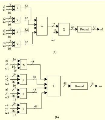
X 16 16 X 16 16 X 16 16 X 16 16 32 32 32 32 + X 32 16 wk 48 Round 16 yk c1 x1 c2 x2 c3 x3 c4 x4 X 16 16 48 48 48 48 48 Round 16 xn 16 X 16 16 16 X 16 16 16 X 16 16 16 (a) (b) c1 y1 w1 c2 y2 w2 c3 y3 w3 c4 y4 w4 +
1D IDCT. The original data is 8 bit, and we simply convert it to 16-bit data for calculation of the 2D DCT, and there is a round block for reducing the overflow bits. After multiplying by cosine coefficients and summing them together as shown in Fig. 3(a), we get 32-bit data. After multiplying the 32-bit data with the DCT coefficient wk, we get 48-bit data. The 48-bit data is rounded off to get 16-bit data yk for the next process. To obtain an inverse transform as in Fig. 3(b), the multiplication and rounding-offs are made for obtaining 16-bit data xn from 48-bit data since the system inputs work in 16-bit format.
IV. Measurement and Simulation Results
The optical printed circuit board (OPCB) used for video
Fig. 4. Photograph of OPCB. Optical link Video in Video out Decoder Encoder FPGA Tx FPGA Rx
streaming is shown in Fig. 4. It has a camera input, a decoder, an FPGA transmitter (Tx), an FPGA receiver (Rx), and an encoder for video streaming output. When a video signal enters into camera input, it is then converted to 8-bit YCbCr (Y- luminance, C-chrominance) components. The standard for the signal is International Telecommunication Union – Radiocommunication Sector (ITU-R) 601 compatible output format digital signal. Input analog S-video is converted to a digital 8-bit signal by the decoder, TW9903, and transmitted through the optical link. At the receiver side, the digital signal is passed to the encoder and the video signal is converted back to analog by the encoder, CS4954. Time consumption and performance of the algorithm is checked using MATLAB. The elapsed time for the 2D DCT algorithm is 3.46 s, and for 2D DCT with Haar’s algorithm, it is 6.9 s. These are implemented to remove the flicker noise and randomly scattered noise all over image content.
Figures 5(a) and 5(b) show the DCT by row and by column. At first, there was no difference between the normalized, ideal, and simulated samples by row. After applying DCT by column, there occurred a slight difference between the normalized, ideal, and simulated samples. We rounded them off as shown in Figs. 3(a) and 3(b), dropping the least significant bits and leaving only the most significant 16 bits. After rounding off, the
Fig. 5. Simulation results of 2D DCT comparing to ideal values: (a) DCT by row, (b) DCT by column, and (c) buffering time for different 2D DCT size. 1 2 3 4 –1.5 –1.0 –0.5 0 0.5 1.0 Sample size
Normailized error dif
ference Simulated Ideal 1 2 3 4 –4 –3 –2 –1 0 1 Sample size
Normailized error dif
fer ence Simulated Ideal (a) (b) 0×0 4×4 8×8 16×16 32×32 64×64 0 0.2542 0.5084 1.0169 2.0338 4.0676 2D DCT block Buf fer time (ms ) (c)
ETRI Journal, Volume 34, Number 1, February 2012 Jamshid Sangirov et al. 125
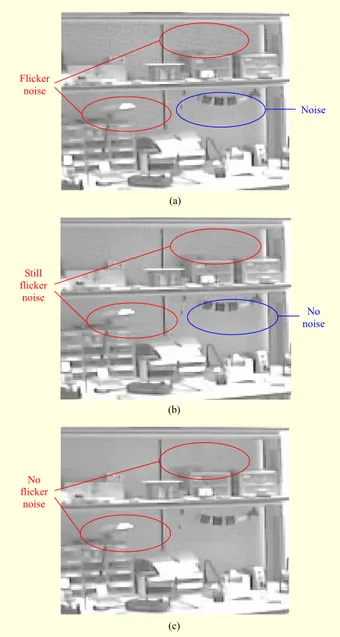
Fig. 6. Captured video images: (a) without denoising and deflickering, (b) after applying denoising, and (c) after applying flicker reduction.
Flicker noise Noise No noise (a) (b) (c) Still flicker noise No flicker noise
result can be seen by normalizing the error difference from Fig. 5(b), and this shows that there occurred a slight change in the image. It is obvious that when rounding off, a high degree of accuracy should be maintained so as not to lose a large portion of information while processing data samples which might harm the overall performance. The analysis for buffer delay and root mean square error for different sizes of DCT blocks are done for comparing the performance of the system. Figure 5(c) shows the buffering time for different 2D DCT blocks in milliseconds. As the block size is changing, the buffering time along with data size increases. Therefore, the 4×4 2D DCT block size is optimal for reducing buffering capacity for synchronization.
Figure 6 shows the images before and after applying the image enhancement algorithm.
V. Conclusion
Synchronization technology was proposed for data transmission in an optical interconnection system. An electrical link was used for the low bandwidth control and clock transmission to reduce the optical point-to-point interconnection. This eliminates the need for a clock and data recovery circuit. Thus, the synchronization method can reduce the overall cost of the optical system. To improve the signal quality, a flicker removal and denoising algorithm has been utilized. Time consumption and performance of the algorithm have been checked using MATLAB, and hardware implementation is done for clock periodicity of synchronization and algorithm functioning. OPCB-based video streaming has been demonstrated, and images have been captured with Labview from real time video transmission for performance analysis of the algorithm. The proposed synchronization technology using a flicker removal and denoising algorithm was designed for optically and electrically interconnected chips.
References
[1] M.S.M. Shirazy et al., “Signal Latency Evaluation and Signal Synchronization for Electrically and Optically Linked Interconnections,” Proc. ICACT, vol. 3, 2008, pp. 2161-2165S. [2] S. Kanumuri et al., “Temporal Flicker Reduction and Denoising
in Video Using Sparse Directional Transforms,” Proc. SPIE, San Diego, CA, vol. 7073, 2008, pp. 70730M-1-11.
[3] J.L. Starck et al., “The Curvelet Transform for Image Denoising,”
IEEE Trans. Image Process., vol. 11, no. 6, June 2002, pp.
670-684.
[4] Y. Kuszpet et al., “Post-processing for Flicker Reduction in H.264/AVC,” Proc. Picture Coding Symp., Lisbon, Portugal, Nov. 2007.
[5] H. Abbas and L.J. Karam, “Suppression of Mosquito Noise by Recursive Epsilon-Filters,” Proc. IEEE ICASSP, Honolulu, Hawaii, Apr. 2007, pp. I-773-I-776.
[6] V. Naranjo and A. Albiol, “Flicker Reduction in Old Films,” Proc.
IEEE ICIP, Vancouver, Canada, Sept. 2000, pp. 657-659.
[7] The Optimization of Discrete Cosine Transform.