P1-70 / W. Choi
IMID 2009 DIGEST •
Abstract
We developed a novel patterning method of organic light emitting materials using a laser-inscribed sacrificial layer for fabricating high-resolution pixels in organic light emitting displays (OLEDs). Our patterning process is capable of achieving high spatial resolution of about 10 µm. Moreover, it has no detrimental effect on the electrical properties of organic materials. This patterning approach is expected to be applicable for patterning and integrating a wide range of organic materials for organic electronic and optoelectronic devices.
1. Introduction
Recently, organic light emitting displays (OLEDs) have extensively been studied for use as a variety of high-performance displays. For high-definition display applications, a precise patterning method of organic light emitting materials is inevitably required for fabricating high-resolution pixel patterns in a lateral array form. Numerous approaches to patterning of organic materials have been proposed [1, 2] but most of them have shown intrinsic problems in pattern resolution or reliability. Thus, a new patterning method suitable for the fabrication of pixel arrays in the OLEDs needs to be developed.
In this work, we developed a simple and versatile patterning method of organic light emitting materials for high-resolution pixel arrays of the OLEDs. This patterning method is based on the conventional lift-off process in combination with the laser-inscription of a fluoro-polymer sacrificial layer. We achieved the feature resolution of about 10 µm and the chemical compatibility with a wide range of organic materials. The OLED fabricated using our patterning method shows stable electroluminescent characteristics.
2. Experimental
The patterning process of pixel arrays in the OLEDs using a laser-inscribed sacrificial layer is schematically illustrated in Fig. 1. A sacrificial layer of a class of the fluoro-polymer is coated on a substrate, and subsequently cured at room temperature. In this experiment, a sacrificial layer can be easily produced from a fluoro-polymer solution through a simple dip-coating process due to the low boiling temperature of the fluoro-solvent which dissolves the fluoro-polymer. The desired pixel areas to be patterned are directly inscribed by selective ablation of the fluoro-polymer layer using an excimer laser illuminating through a predefined photomask. The organic light emitting material is then deposited on the
Fabrication of High-Resolution Pixels in Organic
Light-Emitting Displays Using Laser-Inscribed Sacrificial Layer
Wonsuk Choi, Min-Hoi Kim, Yu-Jin Na, Kyungmo Koo, and Sin-Doo Lee
School of Electrical Engineering, Seoul National University, Kwanak P.O. Box 34, Seoul 151-600, Korea
TEL:82-2-880-1772, e-mail: [email protected]
Keywords: organic light emitting display, pixel array, patterning, laser-inscription
Figure 1. The patterning process of pixel arrays in a OLED device using laser-inscribed sacrificial layer. (a) a fluoro-polymer layer is coated on a glass substrate as a sacrificial layer, (b) the pixel areas to be patterned are directly inscribed by selective laser-ablation of the sacrificial layer, (c) the organic material is deposited on the entire substrate, (d) the pixel patterns are formed by lifting-off the sacrificial layer using a fluoro-solvent.
P1-70 / W. Cho
• IMID 2009 DIGES
entire substrate having the inscribed sacrificial layer. The pixel patterns of organic light emitting materials are finally formed by lifting-off the sacrificial layer together with the remaining organic materials by using a fluoro-solvent.
3. Results and discussion
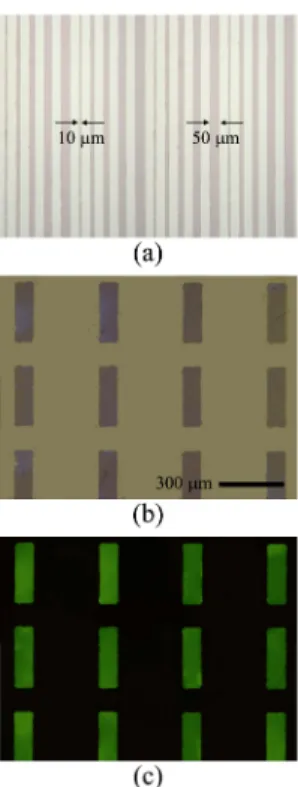
Figure 2 shows examples of patterned organic light emitting materials formed over an area of a few square centimeters on a glass substrate by using laser-inscribed sacrificial layer. In Fig. 2(a) the line arrays with the width from 10 µm to 50 µm are shown. The square pixel arrays of organic materials with green emission observed with optical and fluorescent microscopes are also presented in Fig. 2(b) and 2(c), respectively. The size of each pixel was measured to be 100 µm by 300 µm, which is similar to the typical size of a pixel in a display device. The feature resolution of organic light emitting material patterns, shown in Fig. 2, can be down to a sub-micrometer range depending on the resolution of photomask, in principal. Such high-resolution is expected to be
useful for the fabrication of high-definition displays or the integration of disparate organic electronic elements.
Moreover, our process has no detrimental effect on the electrical properties of organic materials during the processes due to the use of a fluoro-polymer and a fluoro-solvent, that are known to be chemically inert to a variety of organic materials, as a sacrificial layer and an agent for lift-off process. It is clearly seen in two types of OLEDs, that were fabricated under same condition except the patterning methods of organic light emitting materials, one of which was patterned by our lift-off process and the other by deposition through a shadow mask. As shown in Fig. 3, no essential difference in the electroluminescent characteristics between the two OLED devices was observed for given applied voltages. The inset also shows that the emissions from the two OLEDs have same level of the intensity. It is then concluded that our patterning method using a laser-inscribed sacrificial layer is chemically compatible to patterning of organic materials.
4. Summary
We developed a novel method of patterning organic materials by using a laser-inscribed sacrificial layer for high-resolution patterns, and demonstrated the fabrication of organic light emitting pixel arrays. Since our patterning method has the chemical compatibility with various organic materials as well as the possibility of sub-micrometer patterning, our approach would provide a viable platform to fabricate organic arrays for various organic electronic applications including the OLEDs and organic thin film transistors.
Figure 3. (a) The electroluminescent characteristics of two OLED devices fabricated by our patterning method and the conventional shadow mask process.
Figure 2. The images of patterned organic light emitting materials, (a) line array with the width of 10~50 µm, (b) square pixel array (each pixel of 100 µm by 300 µm), (c) fluorescent microscopic image
P1-70 / W. Choi
IMID 2009 DIGEST •
5. References
1. D. G. Lidzey, M. Voigt, C. Giebeler, A. Buckley, J. Wright, K. Bohlen, J. Fieret, and R. Allott, Org. Electron., 6, 221 (2005).
2. H. S. Hwang, A. A. Zakhidov, J.-K. Lee, X. Andre, J. A. DeFranco, H. H. Fong, A. B. Holmes, G. G. Malliaras, and C. K. Ober, J. Mater. Chem., 18, 3087 (2008)