N A N O E X P R E S S
Open Access
Tailoring the Mesoscopic TiO
2
Layer:
Concomitant Parameters for Enabling
High-Performance Perovskite Solar Cells
Taehyun Hwang
1†, Sangheon Lee
1†, Jinhyun Kim
1, Jaewon Kim
1, Chunjoong Kim
2, Byungha Shin
3and Byungwoo Park
1*Abstract
Architectural control over the mesoporous TiO2film, a common electron-transport layer for organic-inorganic
hybrid perovskite solar cells, is conducted by employing sub-micron sized polystyrene beads as sacrificial template. Such tailored TiO2layer is shown to induce asymmetric enhancement of light absorption notably in the
long-wavelength region with red-shifted absorption onset of perovskite, leading to ~20% increase of photocurrent and ~10% increase of power conversion efficiency. This enhancement is likely to be originated from the enlarged CH3NH3PbI3(Cl) grains residing in the sub-micron pores rather than from the effect of reduced perovskite-TiO2
interfacial area, which is supported from optical bandgap change, haze transmission of incident light, and one-diode model parameters correlated with the internal surface area of microporous TiO2layers. With the templating
strategy suggested, the necessity of proper hole-blocking method is discussed to prevent any direct contact of the large perovskite grains infiltrated into the intended pores of TiO2scaffold, further mitigating the interfacial
recombination and leading to ~20% improvement in power conversion efficiency compared with the control device using conventional solution-processed hole blocking TiO2. Thereby, the imperatives that originate from the
structural engineering of the electron-transport layer are discussed to understand the governing elements for the improved device performance.
Keywords: Perovskite solar cell, Nanostructural engineering, Light management, Modeling, Shunting path Background
Organic-inorganic hybrid perovskites (CH3NH3PbI3) have drawn enormous attentions due to their superior optoelectronic properties and versatilities in applications [1, 2]. For photovoltaic devices, many strategies have been attempted to improve the power-conversion effi-ciency. One among many deals with refining the per-ovskite film itself to reduce the trap states and unwanted electron-hole recombination. Generally, defects in grains or grain boundaries act as trap sites for the charge carriers and consequently decrease the charge collection efficiency [3–6]. Indeed, much effort aimed at the
single-crystal perovskites caused successful results for the high photon-to-charge conversion efficiency [7–10]. Therefore, examining the strategies to control the crystallization for the defect reduction is necessary to achieve better-performing perovskite photovoltaics.
Defect-reduced perovskite films can be realized by directly modifying the perovskite synthesis conditions (e.g., reaction environment, precursor stoichiometry, crystallization atmosphere, etc.) [11–13] or by altering the mesoscopic structure of the underlying layers over which the perovskite film synthesis is conducted. The perovskite films are generally deposited upon meso-scopic scaffolds composed of oxide nanoparticles like TiO2, into which the perovskite precursors infiltrate and form small crystallites whose dimensions are defined by the internal pore size of mother scaffold. Enlarging the pores in the scaffold, and hence, increasing the infil-trated perovskite grains is expected to reduce the defects * Correspondence:[email protected]
†Equal contributors
1Department of Materials Science and Engineering, WCU Hybrid Materials
Program, Research Institute of Advanced Materials, Seoul National University, Seoul 08826, Korea
Full list of author information is available at the end of the article
© The Author(s). 2017 Open Access This article is distributed under the terms of the Creative Commons Attribution 4.0 International License (http://creativecommons.org/licenses/by/4.0/), which permits unrestricted use, distribution, and reproduction in any medium, provided you give appropriate credit to the original author(s) and the source, provide a link to the Creative Commons license, and indicate if changes were made.
by grain boundaries. At the same time, the internal elec-tric field that is formed at the semiconductor junction may further assist the charge separation. Light trapping by the nanostructural engineering will also yield an add-itional merit for the performance enhancement [14].
To exploit the potential benefits of large-sized single crystalline perovskite, we herein controlled the nano-structures of mesoscopic TiO2 layer to infiltrate the enlarged CH3NH3PbI3(Cl) grains. Introduction of sacrifi-cial templates during photoelectrode fabrication, one of the facile methods to obtain the controlled pore size and internal surface area [15–18], was applied to render sub-micron sized pores where the large perovskite grains can be accommodated. The concomitant effect of perovskite crystallinity, perovskite-TiO2 interfacial area, and light trapping was investigated to understand the change of photovoltaic parameters resulted from the templating method. Furthermore, since the templated porous layer with hundred-nanometer large open pores inevitably raises the necessity for the complete compactness of hole-blocking layers against charge recombination at the FTO-perovskite direct contact, an alternative blocking layer was applied, providing additional power-conversion efficiency improvement. The essential issues in nanos-tructural engineering were discussed with the correlated solar-cell parameters.
Methods
Preparation of Polystyrene (PS)-TiO2Mixture Solution The PS-TiO2mixture solution was prepared by mixing the ethanol-based PS solution (PS microsphere with 200 nm in diameter) and the TiO2paste (anatase-phase TiO2nanoparticles with ~20 nm in diameter) with vari-ous ratios (PS/TiO2= 1:10, 1:5, and 1:2 in wt. % ratio). The PS-TiO2 solution was then diluted with identical solvent (PS-TiO2/ethanol = 2:5 in wt. % ratio) for spin-coating. To prepare the bare TiO2solution without poly-styrene for a reference, the TiO2paste was diluted with anhydrous ethanol to the corresponding wt. % ratio.
CH3NH3PbI3(Cl) Deposition
The PbI2coating was performed following our pre-vious report [19]. The 3:1 molar ratio of MAI/PbCl2 in DMF (perovskite precursor solution; 2.64 M of MAI and 0.88 M of PbCl2) was then spin-coated at 2000 rpm for 60 s on the PbI2 pre-coated layer or the TiO2 compact layer and annealed at 100 °C for 50 min. To enhance the coverage and obtain the similar thicknesses of the per-ovskite capping layers in the PS-templated TiO2 cases, spin-coating conditions were optimized. Spin-coating speed was reduced from 6500 to 1500 rpm for PbI2and from 2000 to 1500 rpm for the perovskite precursor so-lution. The precursor concentration was increased (from molar ratio of 2.64:0.88 to 4.08:1.36 between MAI and
PbCl2) with the increased annealing time (from 50 to 135 min), and the optimization was checked in the as-pect of the perovskite crystallization from diffraction. As a control group, molar ratio of 2.64:0.88 between MAI and PbCl2was also used on the 1:10 PS-templated TiO2, and we referred it as“1:10 (unoptimized)” since the per-ovskite did not fully cover the top of the 1:10 PS-templated TiO2. Every perovskite deposition was proc-essed in air.
Solar Cell Fabrication
A fluorine-doped tin oxide (FTO) substrate was cleaned, and the TiO2 compact layer was deposited using the 150 and 300 mM solutions of titanium diisopropoxide bis(acetylacetonate) in 1-butanol through the spin-coating followed by the annealing at 500 °C [20]. Then, the substrate was immersed in a 40 mM TiCl4 aqueous solution and treated in 70 °C oven for 30 min, followed by annealing at 500 °C. Bare TiO2 or PS/TiO2 solution was spin-coated at 2500 rpm for 30 s, and the substrate was annealed at 500 °C to re-move the polystyrene templates. Then, TiCl4 treat-ment was performed again, and MAPbI3(Cl) layer was deposited as mentioned in the previous paragraph. Hole transport layer was coated using the spiro-OMeTAD solution (72.8 mg in 1 mL of chloroben-zene) with the addition of 17.5 μL of Li-TFSI stock solution (520 mg in 1 mL of acetonitrile) and 28.8 μL of tert-butylpyridine [20]. Finally, Au electrode was thermally evaporated.
The TiO2compact layer was separately prepared by rf-magnetron sputtering as an alternative blocking layer [21], instead of using conventional titanium diisopropox-ide bis(acetylacetonate) solution. The deposition was performed using the TiO2target (anatase, 99.99%; 5-cm diameter and 0.6-cm thickness) at room temperature under an Ar atmosphere with the operating pressure of 13 mTorr and rf power of 120 W. Except for the block-ing layer deposition, all the other procedures were exactly identical to the solar cell fabrication conditions described above.
Characterization
The crystal structure was examined by X-ray diffraction (XRD) (D8 Advance: Bruker). The images of secondary electrons and back scattered electrons were collected from field-emission scanning electron microscope (FESEM) (Merlin Compact: Zeiss), with the energy-dispersive X-ray spectroscopy (SEM-EDS). The absorb-ance and transmittabsorb-ance of the films were recorded through a UV-Vis spectrophotometer (Cary 5000: Agi-lent Technologies) with the integrating sphere, and the optical bandgap was evaluated from theα2vs.hν (photon energy) analysis. Photocurrent density-voltage (J-V) curves
were obtained by the solar cell measurement system (K3000: McScience) with a solar simulator (Xenon lamp, air mass (AM) 1.5 at 100 mW cm−2). During the measure-ment, black mask of 0.09 cm2was applied, and the scan rate was fixed to 150 mV s−1(reverse direction).
Results and Discussion
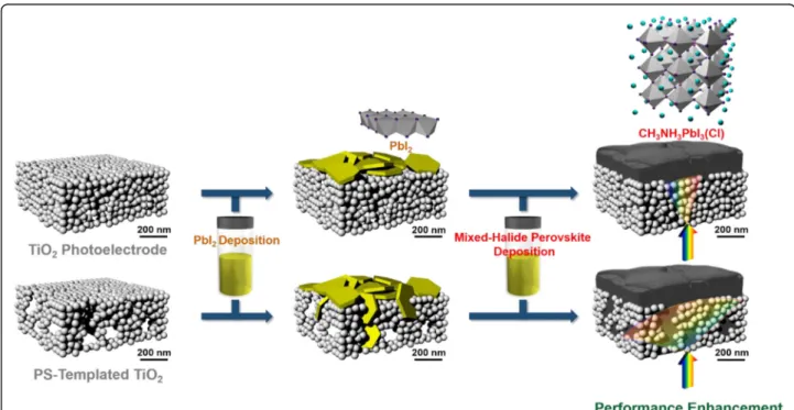
For the achievement of high photon-to-charge conver-sion efficiency in solar cell operation, the high light ab-sorption followed by the electron-hole generation and facile separation of carriers into each electrode should be guaranteed throughout the cell structure. Thus, the essential parameters that can affect these phenomena should be considered [22–25]. For high photoresponsiv-ity, the composition and morphology of MAPbI3can be altered to broaden the absorption spectra [26–29]. For the electron-hole pair separation, internal electric field driven from the semiconductor junction can be utilized, and it is supported by the result that the MAPbI3phase forms the depletion region at the interface with TiO2in approximately hundreds of nanometers [30]. Having suf-ficiently large pores in the scaffold, the size of which is comparable to the depletion layer in the perovskite, therefore shall give a microstructural modification of in-filtrated perovskite grains with the size desirable in terms of electron-hole separation. A comprehensive out-line for the approach suggested above is given in Fig. 1,
depicting the nanostructural engineering of TiO2 accom-panying the perovskite deposition for the intended large crystal infiltration.
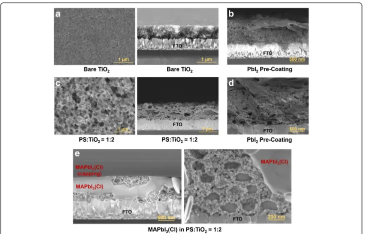
To amend the pore size of TiO2 layers and finally to adjust the grain size of infiltrated perovskite, a sacrificial template is facilely incorporated into the commercially available nanoparticle-based TiO2pastes by mixing with sub-micron sized polystyrene (PS) beads, varying the composition from PS/TiO2= 1:10 to 1:2 [15–18]. Rather thick TiO2porous film (~800 nm) is used for solar cell in this case to investigate the effects of interface between perovskite and TiO2 on the cell performance [2, 22]. Micropores left after the PS removal are successfully filled with PbI2 by the pre-coating step, and the remaining PbI2 crystals are stacked on TiO2 (Fig. 2a–d and Additional file 1: Figure S1). These pre-coating method guarantees the enlarged grains and crystallinity of the converted perovskite since the original PbI6 octa-hedron in the PbI2 structure maintains its framework after the reaction with MA+and I−in the precursor [19]. As shown in Fig. 2e and Additional file 1: Figure S1, layered-PbI2crystals are converted into perovskite, filling the intended ~200-nm micropores. Also, the conversion into MAPbI3(Cl) is completed while maintaining the [110] orientation without remnant, as verified from the diffraction in Fig. 3a (magnification in Additional file 1: Figure S2(a)).
Fig. 1 Schematic diagram illustrating the deposition of mixed-halide perovskite on the nanostructure-tailored TiO2scaffold. Upper row is the
MAPbI3(Cl) deposition on the general mesoporous TiO2substrate. Lower is similar except for the nanostructural engineering of TiO2using
polystyrene (PS) as a sacrificial template. Yellow crystals are PbI2consisting of the edge-sharing of PbI6octahedrons, and black crystals are
The back-scattered electron (BSE) imaging is a useful tool to identify the compositional contrast which origi-nates from the atomic-number difference [31]. The BSE images in Additional file 1: Figure S3 confirm that regu-lar ellipsoidal perovskites are clearly formed in the intended micropores. Furthermore, it is used to confirm the PbI2pre-coating influence on the perovskite infiltra-tion into the mesoporous TiO2 layer (mp-TiO2) [32]. The PbI2 pre-coating indeed do not interfere with the perovskite infiltration into the mp-TiO2 (without PS) based on the BSE intensity comparison between Additional file 1: Figure S3(b) and (c). This is further examined by the elemental mapping (SEM-EDS): the distributions of Pb and I are the same whether the PbI2pre-coating is performed or not (Additional file 1: Figure S4(a) and (b)) and whether the TiO2layer is al-tered by the PS sacrificial template or not (Additional file 1: Figure S4(b) and (c)). The BSE intensity and the EDS mapping confirm that the interfacial area between the perovskite and TiO2 is decreased with the in-creased PS fraction, since the nanoparticulated-TiO2 film consisting of ~20 nm-sized-nanoparticle has a larger
internal surface than the TiO2 film with the intended ~200-nm micropores. The enlarged perovskite grain by PS incorporation is supported accordingly from the above results.
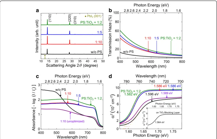
Haze transmission is the ratio of the diffused trans-mittance to the total transtrans-mittance, and discloses the degree of incident light scattering [33]. The PS-templated TiO2 looks opaque, and the haze increases as the PS ratio rises (Fig. 3b). Also, asymmetric eleva-tion of absorbance is observed from MAPbI3(Cl) with increasing PS ratio as shown in Fig. 3c. This is due to the increased light scattering from TiO2 and per-ovskite by the intended large crystals. In addition, the bandgap of mixed-halide perovskite is red-shifted by ~10 meV from the Tauc plot (Fig. 3d). This optical bandgap change is also observed when the identical mixed-halide precursor solution is used for the bare and 1:10 cases (“unoptimized” which is explained in the experimental section). This red-shift is not from the different quantity of Cl since the (110) peak of MAPbI3(Cl) is identical between the bare and 1:10 case (Additional file 1: Figure S2(b)) [34].
Fig. 2 Scanning electron microscopy images showing the TiO2nanostructures with the PbI2pre-coating and MAPbI3(Cl) infiltration into the
polystyrene-templated TiO2scaffold. a Plan and cross-sectional view of bare TiO2. b PbI2-pre-coated bare TiO2. c Plan and cross-sectional view of
TiO2made from the 1:2 wt. % ratio of PS/TiO2(PS/TiO2= 1:2). d PbI2-pre-coated TiO2from PS/TiO2= 1:2. e Cross section of MAPbI3(Cl) in TiO2and
When the concentration of mixed-halide solution is increased by ~50% while maintaining the MAI/PbCl2 ra-tio as 3:1 to improve the perovskite coverage for the PS-templated TiO2 cases, the (110) peak shifts to the high scattering angle (Additional file 1: Figure S2(a), identical to Fig. 3a with proper magnification). The lattice parame-tersa and c in tetragonal (space group I4/m) are changed, respectively, from 0.892 to 0.886 nm and from 1.261 to 1.251 nm. The apparent optical bandgap can vary by the Cl concentration in MAPbI3(Cl), Burstein-Moss effect (carrier concentration), quantum confinement effect, and/or grains and grain boundaries [9, 10, 26, 35–37]. The Burstein-Moss and quantum confinement effects are not pertinent to this system considering that the composition of perovskite was confirmed to be the same for all the cases, and the grain size was out of the regime where the quantum confinement effect works in [36, 37]. Therefore, the optical bandgap change is ex-pected to be caused by the increased perovskite crystal sizes and Cl concentrations (based on the tetragonal unit-cell size). To verify the grain-size effect on the absorption
shift, MAPbI3(Cl) perovskite is deposited with the identi-cal concentration of mixed-halide solution to the bare (without PS) on planar TiO2 layer (Additional file 1: Figure S5). From the diffraction and SEM images of MAPbI3(Cl) film, MAPbI3(Cl) grown on the TiO2planar layer exhibits micrometer-sized lateral grains with the ~30-meV red-shift compared to the bare (without PS) in the absorption onset (inset in Fig. 3d), and this addition-ally supports the absorption-edge shift with respect to the perovskite grain size.
The MAPbI3(Cl) solar cells are fabricated on each PS-templated TiO2 with varying PS ratios (Fig. 4 and Additional file 1: Figure S6) to understand the grain size and interfacial effects on the solar cell perform-ance. The best and the average values of short-circuit current density (Jsc), open-circuit voltage (Voc), fill factor (FF), and power-conversion efficiency (η) are summarized in Table 1. For PS/TiO2= 1:10 case, the η is rather decreased in spite of ~13% improvement of Jsc, which is due to the inferior Voc and FF. Infer-ior Voc in this case should be resolved to overcome
a
b
c
d
Fig. 3 The effect of PS ratio on the nanostructures and optical properties of MAPbI3(Cl) perovskite. a X-ray diffraction of MAPbI3(Cl) films.
b Transmission haze of TiO2with different ratios of PS bead. c Absorbance of MAPbI3(Cl) on the corresponding TiO2, and d the determination of the
optical bandgap for the MAPbI3(Cl) film. Samples are without PS bead (w/o PS), 1:10 wt. % ratio of PS bead in TiO2paste (PS/TiO2= 1:10 (before and
after optimization)), 1:5 wt. % ratio of PS to TiO2(1:5 (optimized)), and 1:2 wt. % ratio (1:2 (optimized)). For comparison, the optical bandgap energy of
the low efficiency, and we have considered several ap-proaches, specifically focusing on the defect reduction that can cause recombination in the perovskite and at the interfaces [38–42]. However, as the PS ratio is in-creased, these parameters are recovered by ~20 mV and ~4% with the additional increase of Jsc, leading to approximately 10% increase of η for the PS/TiO2= 1:2 case compared with the control devices without PS templating.
Analyses of J-V curves based on the one-diode model provide useful parameters helpful to figure out the interfacial effects. The J-V curves are fitted using the ideal one-diode model described in Additional file 1: Figure S7, and the resultant fit curves are shown with the dashed lines in Fig. 4 with the extracted solar-cell parameters in Table 2 [43, 44]. (Fitting results of J-V under dark conditions are shown in Additional file 1: Figure S8.) The fit result shows that the dark-saturation
0.0 0.2 0.4 0.6 0.8 -10 -5 0 5 10 15 20 25 Current Density (mA cm -2 ) Voltage (V) PS:TiO2= 1:2
d
0.0 0.2 0.4 0.6 0.8 -10 -5 0 5 10 15 20 25 PS:TiO2= 1:5 Current Density (mA cm -2 ) Voltage (V)c
0.0 0.2 0.4 0.6 0.8 -10 -5 0 5 10 15 20 25b
PS:TiO2= 1:10 Current Density (mA cm -2 ) Voltage (V) 0.0 0.2 0.4 0.6 0.8 -10 -5 0 5 10 15 20 25a
Current Density (mA cm -2 ) Voltage (V) w/o PSFig. 4 The effect of PS ratio on the performance of the perovskite solar cell. J-V curve (solid line) on a bare TiO2, b 1:10, c 1:5, and d 1:2 PS-templated
TiO2under light exposure (AM 1.5, 100 mW cm−2), and the corresponding fitting result (dashed line) from the ideal one-diode model (described in the
following Additional file 1: Figure S7). The corresponding photovoltaic parameters are summarized in Tables 1 and 2
Table 1 The effect of polystyrene (PS) ratio on the perovskite solar cell performance
Substrate Jsc [mA cm−2] Voc [V] FF [%] η[%] w/o PS 17.9 (16.8) 0.719 (0.713) 53.4 (52.1) 6.87 (6.24) 1:10 20.5 (18.9) 0.633 (0.621) 52.7 (50.8) 6.84 (5.94) 1:5 20.6 (19.3) 0.635 (0.626) 54.5 (53.9) 7.13 (6.51) 1:2 20.5 (19.7) 0.667 (0.644) 56.6 (54.7) 7.74 (6.93)
Short-circuit current density (Jsc), open-circuit voltage (Voc), fill factor (FF), and power-conversion efficiency (η) of perovskite solar cells, without PS and with various ratios of PS-templated TiO2. TiO2blocking layer is deposited by solution. (Data in the bracket are the averaged ones from more than four cells in each condition.)
Table 2 Photovoltaic parameters extracted from the ideal one-diode model Substrate J0 [mA cm−2] Jph [mA cm−2] Rs [Ω cm2] Rsh [Ω cm2] Rshrecom [Ω cm2] n w/o PS 9.39 × 10⁻⁶ (± 3.62 × 10⁻⁶) 18.6 (± 0.1) 5.90 (± 0.19) 152.0 (± 0.8) 152.0 (± 0.8) 1.94 (± 0.05) 1:10 1.92 × 10⁻² (± 0.25 × 10⁻²) 20.6 (± 0.1) 1.69 (± 0.11) 286.6 (± 5.7) 287.2 (± 5.7) 3.53 (± 0.07) 1:5 7.84 × 10⁻³ (± 1.27 × 10⁻³) 20.7 (± 0.1) 1.95 (± 0.11) 303.6 (± 5.8) 304.7 (± 5.8) 3.13 (± 0.07) 1:2 2.77 × 10⁻³ (± 0.67 × 10⁻³) 20.7 (± 0.1) 2.00 (± 0.16) 440.4 (± 10.6) 441.8 (± 10.7) 2.85 (± 0.09)
Dark-saturation current density (J0), photogenerated current density (Jph), series resistance (Rs), shunt resistance (Rsh), recombination shunt resistance (Rshrecom), and ideality factor (n), respectively, from the cell of the highest efficiency in each condition (AM 1.5 at 100 mW cm−2). (Parameters are described in the following Additional file1: Figure S7.)
current density (J0) and the ideality factor (n) are wors-ened from ~10−5 to ~10−3 mA cm−2 and ~2 to ~3, re-spectively, when PS is introduced. The back electron transfer from the FTO front electrode to the perovskite by the ~200-nm penetration may cause the recombin-ation path, as seen in SEM image of Fig. 2e [45].
However, the series resistance (Rs) is improved from 5.9 to 2.0Ω cm2, and the recombination shunt resistance (Rshrecom) (reflectingRshatJph= 0) is increased from 152.0 to 441.8Ω cm2, which may have led to the enhancedFF. As the PS templating reduces the internal surface area by occupying the internal space for TiO2nanoparticle-based porous structure, improvement ofRsandRshrecomcan rea-sonably be postulated to result from the decrease of inter-facial trap sites, which shall be proportional to the internal surface area of TiO2scaffold unless the nature of trap sites at the TiO2-perovskite interface are much affected by PS templating. To check whether such explanation works, the correlation ofRsandRshrecomwith the internal surface area of TiO2layer is plotted in Fig. 5.
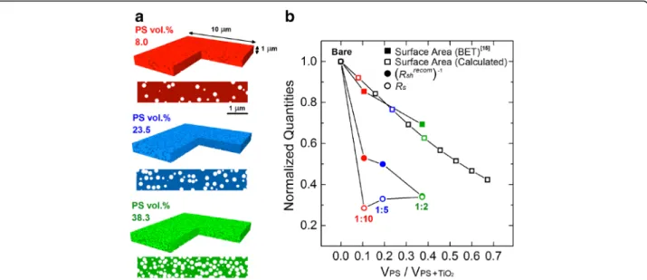
The internal surface area of PS-mediated TiO2 layer for various PS fractions is calculated based on a simple Monte-Carlo method [46], and the possible overlap be-tween beads is considered rather than assuming the beads as hard-sphere. The random distribution of 200-nm spheres in 10 × 10 × 1 μm3 volume is simu-lated by assuming the probability profile of sphere-to-sphere overlap to show exponential decay, the exponent of which is assumed following the Hertzian model of elas-tic potential energy for contact of two idenelas-tical elaselas-tic spheres at a given overlap displacement [47]. A previous report on the surface area change by polystyrene particle templating is also given as a more realistic guidance for comparison. In Fig. 5, the experimental PS/TiO2 weight ratios are converted to volume ratios from the assumed densities of polystyrene (1.05 g cm−3), TiO2(3.91 g cm−3) and porosity of mesoscopic TiO2film (68.1%) [15, 48]. By introducing the PS microbeads, the internal surface area is Fig. 5 Calculated surface area for the analyses of surface area of the PS-templated TiO2and its comparison with the photovoltaic parameters.
a Typical simulation results describing the distribution of 200-nm polystyrene-induced pores with the number variation of PS microspheres (PS vol. %) in 10 × 10 × 1μm3, and the corresponding typical cross-sectional views. b Polystyrene-induced loss of total surface area (open squares), plotted with Rs(series resistance) and Rsh
recom
(recombination shunt resistance) from the experimental J-V curve, as extracted from the ideal one-diode model. (Simulated surface area is also compared to the experimental values from Ref. [15].)
Table 3 The effect of TiO2blocking layer by sputter deposition on the perovskite solar cell performance
Substrate Jsc [mA cm−2] Voc [V] FF [%] η [%] w/o PS 18.3 0.749 55.2 7.56 1:2 20.8 0.694 58.3 8.41
Short-circuit current density (Jsc), open-circuit voltage (Voc), fill factor (FF), and power-conversion efficiency (η) of perovskite solar cells from w/o PS and PS/ TiO2= 1:2. The TiO2blocking layer is deposited by sputtering
Table 4 Photovoltaic parameters from the cells with the TiO2 blocking layer by the sputter deposition
Substrate J0 [mA cm−2] Jph [mA cm−2] Rs [Ω cm2] Rsh [Ω cm2] Rshrecom [Ω cm2] n w/o PS 3.53 × 10⁻⁷ (± 2.93 × 10⁻⁷) 19.0 (± 0.1) 9.53 (± 0.36) 266.7 (± 2.5) 266.7 (± 2.5) 1.64 (± 0.08) 1:2 2.55 × 10⁻³ (± 0.68 × 10⁻³) 20.8 (± 0.1) 2.18 (± 0.22) 460.9 (± 11.2) 467.8 (± 11.5) 2.98 (± 0.09)
Dark-saturation current density (J0), photogenerated current density (Jph), series resistance (Rs), shunt resistance (Rsh), recombination shunt resistance (Rshrecom), and ideality factor (n), respectively (AM 1.5 at 100 mW cm−2)
decreased with the improved Rs and (Rshrecom)−1. The similar dependence of Rs and (Rshrecom)−1 may be from the reduced interfacial traps leading to the decreased resistance of charge transfer or recombination [49]. However, consequently from this simplistic simulation, much drastic variations of Rs and Rshrecom are corre-lated with the morphological engineering. This implies that besides the interfacial effects, other factors like the grain size (crystallinity) and thereby the carrier mobility which is affected by the defects or impurities at the grain boundary should be considered to explain the improvement of Rs and Rshrecom, and thereby re-sultant boost of η [7–9, 50].
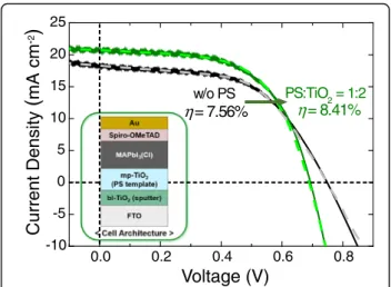
To further increase η, blocking layer deposition method is altered from solution deposition (data in
Tables 1 and 2, Fig. 4, and Additional file 1: Figure S6 and S8) to sputter deposition (Tables 3 and 4, Fig. 6, and Additional file 1: Figure S9) to ensure the compactness. Actually, the SEM images in Additional file 1: Figure S10 confirm the porous morphology by the spin-coating and rather compact structure on each FTO grain by sputtering [48, 51–53]. The modified compact blocking layer results in the enhancement of ~0.3 mA cm−2in Jsc, ~30 mV in Voc, and ~0.7% inη (both bare and PS-templated TiO2), and consequently, approximately 20% increase of η is achieved through the nanostructural control of both blocking and porous layers compared to the bare sample. The compact TiO2hole-blocking layer more effectively in-hibits the direct contact between the FTO and the per-ovskite (preventing the back electron transfer), which is predicted as the origin of charge recombination from the one-diode model. Actually, the modified TiO2 blocking layer leads to the decreasedJ0(recombination current) in both bare and PS cases with the slight improvement in Rshrecom, and these are correlated with the improved Voc andFF as listed in Tables 3 and 4. The performance of the device in this study is not comparable with the state-of-the-art device due to the lowVoc, and the hysteresis prob-lem should be resolved. However, the beneficial optical and electrical properties of perovskite are rationally corre-lated with the nanostructures to elucidate the origin of the enhancedJsc. Furthermore, the principal results from the structural engineering in this work will be applicable for various photovoltaic systems utilizing other metal-oxide-based electron-selective contacts and perovskite composi-tions due to the simplicity of our approach. In addition, the study applying the defect control will further enhance the Voc in this device architecture which already shows the promisingJsc values, potentially improving the device performance even further. As a summary, the effects of
0.0 0.2 0.4 0.6 0.8 -10 -5 0 5 10 15 20 25 η = 7.56%
Voltage (V)
Current Density
(
mA cm
-2)
w/o PS PS:TiO 2= 1:2 η = 8.41%Fig. 6 The effect of TiO2blocking layer by sputter deposition on the
performance of the perovskite solar cell. J-V curve (solid line) under illumination with the corresponding fitting results (dashed line). Photovoltaic parameters are summarized in Tables 3 and 4
Fig. 7 Schematic illustration demonstrating the roles of PS template and TiO2blocking layer on the solar cell performance. The effects of
intended pore engineering in mesoporous TiO2 and the blocking layer are illustrated in Fig. 7.
Conclusions
In this work, the mesoscopic TiO2structure was facilely engineered by using a sacrificial template, and the perovskite solar cells were fabricated on nanostructure-controlled scaffolds by systematically examining the con-comitant key factors of pore engineering that influence the cell performance. The enhanced efficiency by the en-larged pores was attributed to the effectively infiltrated perovskite grains that provided the beneficial light-harvesting features by the absorption enhancement. The perovskite-TiO2interfacial area was rationally correlated with the internal resistances of solar cell and associated with the charge transfer and recombination. Conse-quently, the enlarged perovskite grains with the reduced interfacial area contributed together to the internal resistances, changing direction into the efficiency im-provement. The leakage current that caused the recom-bination was successfully resolved through the compact blocking layer, achieving further performance enhance-ment. We believe that this work suggests a rational nanostructural design of electron-transport layer for high optoelectronic properties in the emerging solar cells.
Additional file
Additional file 1: Figure S1. SEM images showing the TiO2
nanostructures with the PbI2pre-coating and MAPbI3(Cl) infiltration
into the PS-templated TiO2. Figure S2. The effect of PS ratio and the
concentration of precursor solution on the X-ray diffraction of MAPbI3(Cl)
perovskite. Figure S3. Cross-sectional back scattered electron images exhibiting the MAPbI3(Cl) perovskite infiltration in the porous TiO2
layer. Figure S4. Cross-sectional elemental distributions from energy dispersive X-ray spectroscopy (SEM-EDS) showing the Sn, Ti, O, Pb, and I distributions for different porous TiO2scaffolds. Figure S5.
Microstructures of MAPbI3(Cl) on the TiO2blocking layer. Figure S6.
Photovoltaic parameters with the average and the standard deviation in each condition. Figure S7. Ideal one-diode model for the perovskite solar cell. Figure S8. Current density vs. bias under dark and the corresponding fitting results. Figure S9. The effect of TiO2blocking layer by sputter
deposition on the performance of the perovskite solar cell. Figure S10. Morphology comparison by the spin-coating and sputter deposition.
Acknowledgements
This work was supported by the National Research Foundation of Korea (NRF): 2016R1A2B4012938.
Authors’ Contributions
TH and SL carried out the overall scientific experiments and drafted the manuscript. JK (Jinhyun Kim) conducted on optimizing the blocking layer deposition. JK (Jaewon Kim) participated in analyzing the X-ray diffraction. CK and BS helped to improve the logical flows in the manuscript. BP supervised this study and gave valuable advices of scientific logics in detail and finalized the manuscript. All authors read and approved the final manuscript. Competing Interests
The authors declare that they have no competing interests.
Author details
1Department of Materials Science and Engineering, WCU Hybrid Materials
Program, Research Institute of Advanced Materials, Seoul National University, Seoul 08826, Korea.2School of Materials Science and Engineering, Chungnam National University, Daejeon 34134, Korea.3Department of
Materials Science and Engineering, Korea Advanced Institute of Science and Technology, Daejeon 34141, Korea.
Received: 17 October 2016 Accepted: 23 December 2016
References
1. Cho H, Jeong SH, Park MH, Kim YH, Wolf C, Lee CL, Heo JH, Sadhanala A, Myoung N, Yoo S, Im SH, Friend RH, Lee TW (2015) Overcoming the electroluminescence efficiency limitations of perovskite light-emitting diodes. Science 350:1222–1225
2. Jeon NJ, Noh JH, Kim YC, Yang WS, Ryu S, Seok SI (2014) Solvent engineering for high-performance inorganic-organic hybrid perovskite solar cells. Nat Mater 13:897–903
3. Saidaminov MI, Abdelhady AL, Murali B, Alarousu E, Burlakov VM, Peng W, Dursun I, Wang L, He Y, Maculan G, Goriely A, Wu T, Mohammed OF, Bakr OM (2015) High-quality bulk hybrid perovskite single crystals within minutes by inverse temperature crystallization. Nat Commun 6:7586
4. Xu J, Buin A, Ip AH, Li W, Voznyy O, Comin R, Yuan M, Jeon S, Ning Z, McDowell JJ, Kanjanaboos P, Sun J, Lan X, Quan LN, Kim DH, Hill IG, Maksymovych P, Sargent EH (2015) Perovskite–fullerene hybrid materials suppress hysteresis in planar diodes. Nat Commun 6:7081
5. Park HH, Heasley R, Sun L, Steinmann V, Jaramillo R, Hartman K, Chakraborty R, Sinsermsuksakul P, Chua D, Buonassisi T, Gordon RG (2015) Co-optimization of SnS absorber and Zn(O, S) buffer materials for improved solar cells. Prog Photovoltaics 23:901–908
6. Li C, Wu Y, Poplawsky J, Pennycook TJ, Paudel N, Yin W, Haigh SJ, Oxley MP, Lupini AR, Al-Jassim M, Pennycook SJ, Yan Y (2014) Grain-boundary-enhanced carrier collection in CdTe solar cells. Phy Rev Lett 112:156103 7. Tian W, Zhao C, Leng J, Cui R, Jin S (2015) Visualizing carrier diffusion in
individual single-crystal organolead halide perovskite nanowires and nanoplates. J Am Chem Soc 137:12458–12461
8. Shi D, Adinolfi V, Comin R, Yuan M, Alarousu E, Buin A, Chen Y, Hoogland S, Rothenberger A, Katsiev K, Losovyj Y, Zhang X, Dowben PA, Mohammed OF, Sargent EH, Bakr OM (2015) Low trap-state density and long carrier diffusion in organolead trihalide perovskite single crystals. Science 347:519–522 9. Nie W, Tsai H, Asadpour R, Blancon JC, Neukirch AJ, Gupta G, Crochet JJ,
Chhowalla M, Tretiak S, Alam MA, Wang HL, Mohite AD (2015) High-efficiency solution-processed perovskite solar cells with millimeter-scale grains. Science 347:522–525
10. Yin WJ, Chen H, Shi T, Wei SH, Yan Y (2015) Origin of high electronic quality in structurally disordered CH3NH3PbI3and the passivation effect of Cl and O
at grain boundaries. Adv Electron Mater 1:1500044
11. Xie FX, Zhang D, Su H, Ren X, Wong KS, Gratzel M, Choy WCH (2015) Vacuum-assisted thermal annealing of CH3NH3PbI3for highly stable and
efficient perovskite solar cells. ACS Nano 9:639–646
12. Raga SR, Jung MC, Lee MV, Leyden MR, Kato Y, Qi Y (2015) Influence of air annealing on high efficiency planar structure perovskite solar cells. Chem Mater 27:1597–1603
13. Liu J, Shirai Y, Yang X, Yue Y, Chen W, Wu Y, Islam A, Han L (2015) High-quality mixed-organic-cation perovskites from a phase-pure non-stoichiometric intermediate (FAI)1− x-PbI2for solar cells. Adv Mater 27:4918–4923
14. Grandidier J, Weitekamp RA, Deceglie MG, Callahan DM, Battaglia C, Bukowsky CR, Ballif C, Grubbs RH, Atwater HA (2013) Solar cell efficiency enhancement via light trapping in printable resonant dielectric nanosphere arrays. Phys Status Solidi A-Appl Mat 210:255–260
15. Pham TTT, Bessho T, Mathews N, Zakeeruddin SM, Lam YM, Mhaisalkar S, Gratzel M (2012) Light scattering enhancement from sub-micrometer cavities in the photoanode for dye-sensitized solar cells. J Mater Chem 22:16201–16204
16. Cheng C, Lee MM, Noel NK, Hughes GM, Ball JM, Assender HE, Snaith HJ, Watt AAR (2014) Polystyrene templated porous titania wells for quantum dot heterojunction solar cells. ACS Appl Mater Inter 6:14247–14252 17. Horantner MT, Zhang W, Saliba M, Wojciechowski K, Snaith HJ (2015)
Templated microstructural growth of perovskite thin films via colloidal monolayer lithography. Energy Environ Sci 8:2041–2047
18. Song X, Wang M, Xing T, Deng J, Ding J, Yang Z, Zhang X (2014) Fabrication of micro/nano-composite porous TiO2electrodes for quantum dot-sensitized
solar cells. J Power Sources 253:17–26
19. Hwang T, Cho D, Kim J, Kim J, Lee S, Lee B, Kim KH, Hong S, Kim C, Park B (2016) Investigation of chlorine-mediated microstructural evolution of CH3NH3PbI3(Cl) grains for high optoelectronic responses. Nano Energy
25:91–99
20. Kim J, Hwang T, Lee S, Lee B, Kim J, Jang GS, Nam S, Park B (2016) Solvent and intermediate phase as boosters for the perovskite transformation and solar cell performance. Sci Rep 6:25648
21. Kim J, Choi H, Nahm C, Moon J, Kim C, Nam S, Jung DR, Park B (2011) The effect of a blocking layer on the photovoltaic performance in CdS quantum-dot-sensitized solar cells. J Power Sources 196:10526–10531 22. Heo JH, You MS, Chang MH, Yin W, Ahn TK, Lee SJ, Sung SJ, Kim DH,
Im SH (2015) Hysteresis-less mesoscopic CH3NH3PbI3perovskite hybrid
solar cells by introduction of Li-treated TiO2electrode. Nano Energy
15:530–539
23. Lin CH, Chattopadhyay S, Hsu CW, Wu MH, Chen WC, Wu CT, Tseng SC, Hwang JS, Lee JH, Chen CW, Chen CH, Chen LC, Chen KH (2009) Enhanced charge separation by sieve-layer mediation in high-efficiency inorganic-organic solar cells. Adv Mater 21:759–763
24. McDaniel H, Heil PE, Tsai CL, Kim K, Shim M (2011) Integration of type II nanorod heterostructures into photovoltaics. ACS Nano 5:7677–7683 25. Maitani MM, Tanaka K, Mochizuki D, Wada Y (2011) Enhancement of
photoexcited charge transfer by {001} facet-dominating TiO2nanoparticles.
J Phys Chem Lett 2:2655–2659
26. Im JH, Jang IH, Pellet N, Gratzel M, Park NG (2014) Growth of CH3NH3PbI3
cuboids with controlled size for high-efficiency perovskite solar cells. Nat Nanotechnol 9:927–932
27. Lee JW, Lee SH, Ko HS, Kwon J, Park JH, Kang SM, Ahn N, Choi M, Kim JK, Park NG (2015) Opto-electronic properties of TiO2nanohelices with embedded
HC(NH2)2PbI3perovskite solar cells. J Mater Chem A 3:9179–9186
28. Noh JH, Im SH, Heo JH, Mandal TN, Seok SI (2013) Chemical management for colorful, efficient, and stable inorganic-organic hybrid nanostructured solar cells. Nano Lett 13:1764–1769
29. Todorov T, Gershon T, Gunawan O, Sturdevant C, Guha S (2014) Perovskite-kesterite monolithic tandem solar cells with high open-circuit voltage. Appl Phys Lett 105:173902
30. Aharon S, Gamliel S, Cohen BE, Etgar L (2014) Depletion region effect of highly efficient hole conductor free CH3NH3PbI3perovskite solar cells. Phys
Chem Chem Phys 16:10512–10518
31. Goldstein JI, Lyman CE, Newbury DE, Lifshin E, Echlin P, Sawyer L, Joy DC, Michael JR (2003) Scanning electron microscopy and X-ray microanalysis, 3rd edn. Kluwer Academic, Plenum Publishers. http://www.springer.com/us/ book/9780306472923
32. Divitini G, Cacovich S, Matteocci F, Cina L, Carlo AD, Ducati C (2016) In situ observation of heat-induced degradation of perovskite solar cells. Nat Energy 1:15012
33. Lee W, Hwang T, Lee S, Lee SY, Kang J, Lee B, Kim J, Moon T, Park B (2015) Organic-acid texturing of transparent electrodes toward broadband light trapping in thin-film solar cells. Nano Energy 17:180–186
34. Li Y, Sun W, Yan W, Ye S, Peng H, Liu Z, Bian Z, Huang C (2015) High-performance planar solar cells based on CH3NH3PbI3-xClxperovskites with
determined chlorine mole fraction. Adv Funct Mater 25:4867–4873 35. Colella S, Mosconi E, Fedeli P, Listorti A, Gazza F, Orlandi F, Ferro P, Besagni T,
Rizzo A, Calestani G, Gigli G, Angelis FD, Mosca R (2013) MAPbI3-xClx mixed halide perovskite for hybrid solar cells: the role of chloride as dopant on the transport and structural properties. Chem Mater 25:4613–4618
36. Manser JS, Kamat PV (2014) Band filling with free charge carriers in organometal halide perovskites. Nat Photonics 8:737–743
37. Di D, Musselman KP, Li G, Sadhanala A, Ievskaya Y, Song Q, Tan ZK, Lai ML, MacManus-Driscoll JL, Greenham NC, Friend RH (2015) Size-dependent photon emission from organometal halide perovskite nanocrystals embedded in an organic matrix. J Phys Chem Lett 6:446–450
38. Wendt S, Sprunger PT, Lira E, Madsen GKH, Li Z, Hansen JØ, Matthiesen J, Blekinge-Rasmussen A, Lægsgaard E, Hammer B, Besenbacher F (2008) The role of interstitial sites in the Ti3d defect state in the band gap of titania. Science 320:1755–1759
39. Liu D, Li S, Zhang P, Wang Y, Zhang R, Sarvari H, Wang F, Wu J, Wang Z, Chen ZD (2017) Efficient planar heterojunction perovskite solar cells with Li-doped compact TiO2layer. Nano Energy 31:462–468
40. Yin WJ, Shi T, Yan Y (2014) Unusual defect physics in CH3NH3PbI3perovskite
solar cell absorber. Appl Phys Lett 104:063903
41. Leijtens T, Eperon GE, Barker AJ, Grancini G, Zhang W, Ball JM, Kandada ARS, Snaith HJ, Petrozza A (2016) Carrier trapping and recombination: the role of defect physics in enhancing the open circuit voltage of metal halide perovskite solar cells. Energy Environ Sci 9:3472–3481
42. Li Z, Tinkham J, Schulz P, Yang M, Kim DH, Berry J, Sellinger A, Zhu K (2016) Acid additives enhancing the conductivity of spiro-OMeTAD toward high-efficiency and hysteresis-less planar perovskite solar cells. Adv Energy Mater 6:1601451
43. Choi H, Hwang T, Lee S, Nam S, Kang J, Lee B, Park B (2015) The construction of tandem dye-sensitized solar cells from chemically-derived nanoporous photoelectrodes. J Power Sources 274:937–942
44. Aitola K, Sveinbjornsson K, Correa-Baena JP, Kaskela A, Abate A, Tian Y, Johansson EMJ, Gratzel M, Kauppinen EI, Hagfeldt A, Boschloo G (2016) Carbon nanotube-based hybrid hole-transporting material and selective contact for high efficiency perovskite solar cells. Energy Environ Sci 9:461–466 45. Chen X, Yang S, Zheng YC, Chen Y, Hou Y, Yang XH, Yang HG (2015)
Multifunctional inverse opal-like TiO2electron transport layer for efficient
hybrid perovskite solar cells. Adv Sci 2:1500105
46. Lee S, Flanagan JC, Kang J, Kim J, Shim M, Park B (2015) Integration of CdSe/CdSexTe1−xtype-II heterojunction nanorods into hierarchically porous
TiO2electrode for efficient solar energy conversion. Sci Rep 5:17472
47. Johnson KL, Kendall K, Roberts AD (1971) Surface energy and the contact of elastic solids. Proc R Soc Lond A 324:301–313
48. Kang SH, Lim JW, Kim HS, Kim JY, Chung YH, Sung YE (2009) Photo and electrochemical characteristics dependent on the phase ratio of nanocolumnar structured TiO2films by rf magnetron sputtering technique.
Chem Mater 21:2777–2788
49. Hau SK, Yip HL, Acton O, Baek NS, Ma H, Jen AKY (2008) Interfacial modification to improve inverted polymer solar cells. J Mater Chem 18:5113–5119 50. Wang Y, Li S, Zhang P, Liu D, Gu X, Sarvari H, Ye Z, Wu J, Wang Z, Chen ZD
(2016) Solvent annealing of PbI2for the high-quality crystallization of
perovskite films for solar cells with efficiencies exceeding 18%. Nanoscale 8:19654–19661
51. Moehl T, Im JH, Lee YH, Domanski K, Giordano F, Zakeeruddin SM, Dar MI, Heiniger LP, Nazeeruddin MK, Park NG, Gratzel M (2014) Strong photocurrent amplification in perovskite solar cells with a porous TiO2
blocking layer under reverse bias. J Phys Chem Lett 5:3931–3936 52. Chen C, Cheng Y, Dai Q, Song H (2015) Radio frequency magnetron
sputtering deposition of TiO2thin films and their perovskite solar cell
applications. Sci Rep 5:17684
53. Ge S, Xu H, Wang W, Cao R, Wu Y, Xu W, Zhu J, Xue F, Hong F, Xu R, Xu F, Wang L, Huang J (2016) The improvement of open circuit voltage by the sputtered TiO2layer for efficient perovskite solar cell. Vacuum 128:91–98
Submit your manuscript to a
journal and benefi t from:
7 Convenient online submission 7 Rigorous peer review7 Immediate publication on acceptance 7 Open access: articles freely available online 7 High visibility within the fi eld
7 Retaining the copyright to your article
![Table 2 Photovoltaic parameters extracted from the ideal one- one-diode model Substrate J 0 [mA cm −2 ] J ph [mA cm −2 ] R s[ Ω cm 2 ] R sh[ Ω cm 2 ] R sh recom[Ω cm2 ] n w/o PS 9.39 × 10 −6 (± 3.62 × 10 −6 ) 18.6 (± 0.1) 5.90 (± 0.19) 152.0 (± 0.8) 152.0](https://thumb-ap.123doks.com/thumbv2/123dokinfo/5084250.75209/6.892.85.436.862.1031/table-photovoltaic-parameters-extracted-ideal-diode-model-substrate.webp)