2017년 1월 보 고 서 번 호
전체부수
ETRI 주요 사업: 금속-절연체 전이
현상규명 및 응용기술 개발
ETRI Principal Project: Project on Mechanism and application of
Metal-Insulator Transition
인 사 말 씀
ETRI 주요사업은 혁신형 국가 전략기술 개발을 위한 창의연구
수행을 통하여 세계 최고의 원천기술을 단계적으로 확보하고,
노벨상에 버금가는 연구결과 창출을 통한 World Top Class의
정부출연연구소의 위상 달성을 목표로 2016년부터 정부 출연금
사업으로 추진된 전략 사업입니다.
세부과제로 금속-절연체 전이(MIT) 현상규명 및 응용기술
개발을 수행하여 국제원천특허 획득 및 SCI 저널에 연구성과 게재
등의 결과를 가져왔으며, 각 분야 핵심원천기술 창출의 최종목표
달성에 다가가고 있습니다. 본과제가 목표대로 진행되기 위하여
연구가 심화됨에 따른 예산 및 제도적 지원체계를 갖출 수 있도록
더욱 노력할 것입니다.
향후 MIT 창의연구가 목표 이상의 성과를 거둬 물리학의 문제를
해결하여 국가의 위상을 세계 만방에 알리고 또한 미래 원천기술
확보를 통한 미래시장 선점 및 국가기술경쟁력 제고에 획기적으로
기여하고 ETRI 연구개발의 새로운 지평을 열기를 기대합니다.
2016년 1월
한국전자통신연구원 원장 이 상 훈
제 출 문
본 연구보고서는 주요사업인 " 금속-절연체 전이(Metal-Insulator
Transition:MIT) 현상규명 및 응용기술 개발 과제"의 결과로서, 본
과제에 참여한 아래의 연구팀이 작성한 것입니다.
2017년 1월
연구책임자 : 책임연구원 김현탁 (소재부품창의연구실장)
연구참여자 : 연 구 원 테티아나(소재부품창의연구실)
연구참여자 : 연 구 원 조성우 (소재부품창의연구실)
연구참여자 : 연 구 원 정순규 (소재부품창의연구실)
연구참여자 : 연 구 원 조진철* (소재부품창의연구실)
연구참여자 : 교 수 Dimitri N Basov**
(University of California at SanDiego: 국제공동연구)
연구참여자 : 연 구 원 Sternbach Aaron**
(University of California at SanDiego: 국제공동연구)
* 연수생, 위촉연구원, 인턴요 약 문
Ⅰ. 제 목
ETRI
주요
사업,
금속-절연체
전이(Metal-Insulator
Transition:MIT) 현상규명 및 응용기술 개발 과제
Ⅱ. 연구목적 및 중요성
본 연구의 목적은 물리학의 미해결 문제인 금속-전연체 전이
(MIT) 현상을 규명하여 인류발전에 기여한다. MIT 현상규명은 1930 년
대에 금속의 자유전자들 사이에 강한 쿨롱 상호작용(Coulomb
interaction)이 존재하면 금속에서 부도체로 상전이 한다는 위그너
와 모트가 제안한 강상관 MIT 현상은 양자역학적으로 정밀하게 계산
이 되었지만 실험적으로 아직 증명되지 않은 물리문제이다. 그 후
MIT 근방에서 고온초전도, 절연파괴, 자이안트 마그넷티즘 등 새로운
물리현상이 발견되었다. 또 공학적으로는 반도체 소자의 크기를 줄이
면서 나타나는 단채널 효과 (Short channel effect)가 큰 문제로 대
두되었다. 이 문제를 극복하기 위해 반도체 한계극복이라는 큰 이슈
가 등장하였고, 이 문제 해결의 대안으로 반도체보다 저항이 낮은 금
속특성을 이용하는 절연체(부도체, Insulator)-금속(도체, Metal) 전
이가 제안되었다. 본 연구는 학문적 중요성뿐만 아니라 기술적으로도
새로운 패러다임을 바꾸는 반도체 한계를 극복하는 신기술을 창출하
기 때문에 매우 중요하다.
Ⅲ. 연구내용 및 범위
및 MIT 나노기초 핵심응용 기술 개발을 통한 강상관 물질에서 MIT 현
상을 연구하고, 핵심 응용소자로써 MIT 센서, 스위치, 파워 소자 등
을 개발한다. 그리고 개발 된 응용소자를 이용하여 관련 응용 기술
개발을 수행한다. 또한 MIT 현상과 응용에 대한 국제공동연구를 수행
함으로써 MIT 의 학문적 기초와 응용 기술을 더욱 깊이 있게 발전시
키고자 한다.
Ⅳ. 연구결과
MIT 현상규명을 위하여 MIT 물질 VO
2에서 코히런트 포논의 온
도의존성을 조사하여 M2 구조에서 구조 상전이를 겪지 않는 MIT 현상
을 최초로 관측한다. 또 나노 레벨급 광전도도와 라만산란 실험을 동
시에 관측하여 구조상전이 없는 MIT 를 관측한다. 그리고 국제공동연
구로서 나노레벨에서 팸토초 기술로 MIT 현상을 측정하였다.
MIT 의 대표적인 강상관 물질인 VO
2를 Pulsed Laser Deposition(PLD)
방법으로 산소분압을 조절하여 박막을 제조하여 그 박막의 특성을
저항의 온도의존성, SEM 과 XRD 등의 물성 분석을 통해 임계특성의 변
화를 관측조사 한다. 그 박막의 대량생산을 위하여 Si 기판 위에 VO
2Epi 박막을 제조한가.
MIT Critical Temperature Switch(CTS)를 이용하여 MIT 전자개페기와
차단기, MIT CTS 와 NDR 스위칭을 LED 발광에 적용하여 MIT-NDR 현상
을 이용하는 램프를 발명하였다. 자동차 라디에이터 팬모터의 과전류
방지를 위하여 다이오드 레지스터를 새롭게 발명한다.
Ⅴ. 기대성과 및 건의
금속-절연체 전이 현상규명 연구에서 MIT 물질의 M2 구조에서
구조 상전이 없는 MIT를 관측하여 물리학의 문제인 모트 MIT를
밝힌다. MIT 기술 개발을 통해 NDR-MIT 스위칭 기술을 이용하여
형광등 대체용 LED 램프, 자동차 라디에이터 팬모터 제어용 다이오드
레지스터는 상용화 하여 그 분야에서 기술적 발전뿐만 아니라
수출을 하여 국부창출에 기여할 수 있다.
ABSTRACT
Ⅰ. TITLE
ETRI Principal Project: Project on Mechanism and application
of Metal-Insulator Transition
Ⅱ. THE OBJECTIVES
Metal-insulator transition (MIT) is a topic for research
interest in the field of condensed matter physics field.
Experimental and theoretical studies to reveal the mechanism of MIT
have been on-going issue for half a century. There are also
representative device concepts utilizing MIT in VO
2such as
two-terminal electronic switching device, three-terminal (gated)
electronic switches, optical gating devices, field-induced
electrical oscillators, and thermal sensors. Here, the MIT
mechanism and its applications are studied.
Ⅲ. THE CONTENTS AND SCOPE OF THE STUDY
In this research, the MIT mechanism is studied by observing the
MIT and the structural phase-transition phenomena using Femtosecond
technique in a strongly correlated VO
2and nanolevel photocurrent,
Raman scattering, Hall effect, and Thermoelectric effect. As the
MIT application, the LED lamp replacing the fluorescent lamp is
developed by using negative-differential- resistance (NDR) MIT
switching. Moreover, a resistor using power diode, controlling a
speed of radiator fan Motor in Motorcar, is developed.
Ⅳ. RESULTS
phase transition in M2 of a representative strongly correlated VO
2,
observing of coherent phonons using the femtosecond technique,
which is suggested as evidence of the Mott transition. Moreover,
the percolation in M2 is also observed. The MIT not accompanied with
the structural phase transition is observed in a nanolevel by
measuring photocurrent and Raman scattering. The MIT mechanism is
revealed. As the MIT application, the LED lamp replacing the
fluorescent lamp is invented using the NDR-MIT switching. Moreover,
a resistor using power diode, controlling a speed of radiator fan
Motor in Motorcar, is developed.
Ⅴ. EXPECTED RESULT & PROPOSITION
The observation of the MIT not undergoing the structural phase
transition reveals the presence of the correlation in the strongly
correlated material VO
2. Moreover, the inventions of the LED lamp
using the NDR-MIT switching and the diode resistor can contribute
to commercialization of the MIT technologies.
CONTENTS
CHAPTER 1 ETRI PRINCIPAL PROJECT, PROJECT ON MECHANISM AND
APPLICATION OF METAL-INSULATOR TRANSITION ··· 28
SECTION 1 Research Outline ... 28
SECTION 2 Research Objectives ... 28
SECTION 3 Research Systems ... 29
SECTION 4 Report Contents ... 30
CHAPTER 2 2014
··· 31
SECTION 1 Research Objectives ... 31
SECTION 2 Research Results ... 33
1. EFFECT OF OXYGEN PARTIAL PRESSURE ON THE PROPERTIES OF VO
2FILMS
GROWN BY PULSED LASER DEPOSITION METHOD ··· 33
2. MODIFICATION OF METAL-INSULATOR TRANSITION IN VO
2FILMS GROWN
ON TIO
2SUBSTRATES ··· 41
3. THERMOPOWER SWITCHING IN METAL-INSULATOR TRANSITION MATERIALS
··· 46
4. Tungsten doping effect on electrical, structural properties
of V1-xWxO2 (0≤x≤4.0 at.%) thin films and device grown by
Sol-Gel method ··· 53
CHAPTER 3 2015 ··· 67
SECTION 1 Research Objectives ... 67
SECTION 2 Research Results ... 68
1. Measurements of Current vs Time switching speed in the AC MIT
switchgear ··· 68
2. Correlation between electrical and structural properties of
the nanothick VO
2films ··· 74
3. Development of a Magnetic switch using CTS ··· 77
SECTION 3 Research Outputs ... 95
CHPATER 4 2016 ··· 98
SECTION 1 Research Objectives ... 98
SECTION 2 Research Results ... 102
1. Photoheat-Induced Schottky Nanojunction and Indirect Mott
Transition in VO
2: Photocurrent Analysis ··· 102
2. Epitaxial growth of higher transition-temperature VO
2films
on AlN/Si ··· 115
3. Local control of the strain in ultrathin VO
2films by substrate
patterning ··· 127
4. Room temperature stabilization of the M2 phase in strained VO2
films observed by high-resolution transmission electron
microscopy ··· 133
5. In-situ measurements of the phase dynamics in ultrathin VO2
films ··· 137
6. Research and development of a Magnetic switch using CTS 140
7. Research and development of a LED lamp ··· 151
8. 다이오드 레지스터 개발 ··· 163
SECTION 3 Research and development of a Diode-resistor .... 171
CHAPTER 5 Conclusions and Sugestions ··· 173
SECTION 1 Conclusions ... 173
목 차
제 1 장 ETRI 주요 사업, 금속-절연체 전이(METAL-INSULATOR
TRANSITION:MIT) 현상규명 및 응용기술 개발 과제 ··· 28
제 1 절 사업 개요 ... 28
제 2 절 사업 목표 및 내용 ... 28
제 3 절 사업 수행 체계 ... 29
제 4 절 보고서 체계 ... 30
제 2 장 2014 년 금속-절연체 전이 현상규명 및 응용기술 개발 · 31
제 1 절 연구목표 ... 31
제 2 절 연구내용 ... 33
1. EFFECT OF OXYGEN PARTIAL PRESSURE ON THE PROPERTIES OF VO
2FILMS
GROWN BY PULSED LASER DEPOSITION METHOD ··· 33
2. MODIFICATION OF METAL-INSULATOR TRANSITION IN VO
2FILMS GROWN
ON TIO
2SUBSTRATES ··· 41
3. THERMOPOWER SWITCHING IN METAL-INSULATOR TRANSITION MATERIALS
··· 46
4. 솔-겔 법으로 성장된 V
1-xW
xO
2(0≤x≤4.0 at.%)박막에서의 텅스텐
불순물이 미치는 영향과 그 전기적 구조적 특성 및 소자제작
··· 53
제 3 장 2015 년 금속-절연체 전이 현상규명 및 응용기술 개발 · 67
제 1 절 연구목표 ... 67
제 2 절 연구내용 ... 68
1. Measurements of Current vs Time switching speed in the AC MIT
switchgear ··· 68
2. Correlation between electrical and structural properties of
the nanothick VO
2films ··· 74
3. MIT 전자개폐기와 차단기 개발 ··· 77
제 3 절 연구성과 ... 95
제 4 장 2016 년 금속-절연체 전이 현상규명 및 응용기술 개발 · 98
제 1 절 연구목표 ... 98
제 2 절 연구내용 ... 102
1. Photoheat-Induced Schottky Nanojunction and Indirect Mott
Transition in VO
2: Photocurrent Analysis ··· 102
2. Epitaxial growth of higher transition-temperature VO
2films
on AlN/Si ··· 115
3. Local control of the strain in ultrathin VO
2films by substrate
patterning ··· 127
4. Room temperature stabilization of the M2 phase in strained VO2
films observed by high-resolution transmission electron
microscopy ··· 133
5. In-situ measurements of the phase dynamics in ultrathin VO2
films ··· 137
6. 임계온도스위치(CTS)를 활용한 교류전자개폐기 개발 ··· 140
7. LED 형광등 개발 ··· 151
8. 다이오드 레지스터 개발 ··· 163
제 3 절 연구성과 ... 171
제 5 장 결론 및 건의사항 ··· 173
제 1 절 결론 ... 173
제 2 절 건의사항 ... 174
표목차
표 2-1. XPS FIT PARAMETERS FOR V2P AND O1S PEAKS OF VO2 FILMS ON AL2O3 SUBSTRATES ... 39 표 3-1. 정전압 회로가 없는 실험에서 저항변화에 따른 전압 값 (CTS 동작경우) . 81 표 3-2. 정전압 회로가 있는 실험에서 저항변화에 따른 전압 값 (CTS 동작경우) . 82 표 3-3. 저항에 따른 차단 속도 측정. (A) SCR 을 부착하고 DC 전원 공급 후 곧바로
LOAD 를 걸었을 때, (B) DC 전원 공급 5 분뒤 LOAD 를 걸었을 때. (50A) ... 85 표 3-4. CURRENT = 30A, C52XX 합금 WIRE : W = 1.2MM, L = 30MM, T = 0.1MM
... 89 표 3-5. CURRENT = 60A, C52XX 합금 WIRE : W = 1.2MM, L = 30MM, T = 0.1MM
... 89 표 3-6. CURRENT = 60A, PCB TRACE : W = 1MM, L = 30MM, T = 0.203 MM ... 90 표 3-7. 전류에 따른 금속의 온도 측정... 94 표 4-1. CALCULATED LATTICE PARAMETERS FOR VO2 AND ALN AND THEIR
MISMATCH. ... 123 표 4-2. 그림 4-21 에서 SCR 이 TURN ON 될때의 가변 저항 P4, P3 의 저항값.... 142 표 4-3. 그림 4-22 에서 SCR 이 TURN ON 될때의 가변 저항 P1, P2 의 저항값.... 143 표 4-4. 다이오드 레지스터 시험 조건 및 측정결과 ... 167 표 4-5. 전압변동 테스트 결과. ... 169
그림목차
그림 1-1. 연구 수행 체계 ··· 29 그림 2-1. TEMPERATURE DEPENDENCIES OF THE RESISTANCE, NORMALIZED
RESISTANCE (UPPER INSET) AND CORRESPONDING DERIVATIVE CURVE (LOWER INSET, ONLY FOR BEST QUALITY SAMPLES ~40 MTORR) OF THE RESISTANCE FOR VO2 FILMS DEPOSITED ON (A) R-, (B) A-, (C) M- AND (D)
C-PLANE SAPPHIRE SUBSTRATES AT DIFFERENT OXYGEN PARTIAL PRESSURE. THE SOLID AND OPEN CIRCLES REPRESENT TEMPERATURE RAMPING UP AND DOWN, RESPECTIVELY. ··· 35 그림 2-2. PHASE TRANSITION CHARACTERISTICS OF VO2/AL2O3 SAMPLES ··· 36 그림 2-3. SEM IMAGES OF THE SURFACE MORPHOLOGY OF VO2 FILMS ON AL2O3 SUBSTRATES GROWN AT DIFFERENT OXYGEN PARTIAL PRESSURE ··· 37 그림 2-4. XPS SPECTRA (AFTER 100S AR+-SPUTTERING) OF VO2/AL2O3
DEPOSITED AT HIGH OXYGEN PRESSURE ON SUBSTRATES WITH DIFFERENT ORIENTATIONS (A); AT DIFFERENT OXYGEN PRESSURE ON M-PLANE AL2O3 (B) ··· 38 그림 2-5. XRD PATTERNS OF VO2 FILMS DEPOSITED ON SAPPHIRE WITH
DIFFERENT ORIENTATIONS, AT HIGH AND LOW OXYGEN PARTIAL PRESSURE 40 그림 2-6. RESISTANCE VS TEMPERATURE OF THE OF VO2 FILMS DEPOSITED ON
DIFFERENT SUBSTRATES IN DEPENDENCE ON: FILMS THICKNESS D
(SUBSTRATE: TIO2 (001)) (A), SUBSTRATE TEMPERATURE TS (SUBSTRATE: TIO2 (001)) (B), OXYGEN GROWTH PRESSURE P(O2) (SUBSTRATE: TIO2 (001)) (C), SUBSTRATE TEMPERATURE TS (SUBSTRATE: TIO2 (110)) (D), SUBSTRATE ORIENTATIONS FOR FILM THICKNESS 80 NM (SUBSTRATE: AL2O3) (E),
(F) ··· 43 그림 2-7. DERIVATIVE CURVES OF THE RESISTANCE VS. TEMPERATURE FOR
VO2/TIO2 AND VO2/AL2O3 DEMONSTRATING SHIFT OF THE TRANSITION TEMPERATURE TMIT ··· 44 그림 2-8. SEM IMAGE OF SURFACE MORPHOLOGY OF 20 AND 100NM OF VO2
THIN FILMS DEPOSITED ON (001) AND (110) TIO2 SUBSTRATES ··· 44 그림 2-9. XRD PATTERNS OF THE VO2 FILM DEPOSITED ON (001) AND (110) TIO2
SUBSTRATES ··· 45 그림 2-10. XRD (T) PATTERNS OF THE VO2/(001)TIO2 SUBSTRATES ··· 46 그림 2-11. TEMPERATURE DRIVEN METAL-INSULATOR TRANSITION IN VO2 AND
SCHEMATIC DESCRIPTION OF STRUCTURAL PHASE TRANSITION (INSETS) WITH CHANGING V-CATIONS POSITION FROM MONOCLINIC INSULATING M1
TO TETRAGONAL METALLIC R PHASE. CR~2.87Å - V-V DISTANCE IN R
STRUCTURE, Δ – LATTICE DISTORTION (CHARGE-DENSITY WAVE) AND V-V DIMERIZATION DURING R→M1 TRANSITION. ··· 48
그림 2-12. SEM IMAGE OF THE SURFACE MORPHOLOGY OF VO2 FILMS ON P- AND N-TYPE SI SUBSTRATES ··· 49 그림 2-13. XRD PATTERNS OF VO2 FILMS DEPOSITED ON P- AND N-TYPE SI
SUBSTRATES ··· 49 그림 2-14. TEMPERATURE DEPENDENCE OF THE RESISTIVITY OF VO2 FILMS ON
HIGHLY-DOPED P- AND N-TYPE SI SUBSTRATES MEASURED IN LATERAL (A) AND VERTICAL (B) CASES; CORRESPONDING DERIVATIVE CURVES FOR
VO2/P-SI (C) AND VO2/N-SI (D) ··· 50 그림 2-15. SCHEME OF THERMOPOWER MEASUREMENTS: LATERAL (A) AND
VERTICAL (B) GEOMETRY FOR VO2/SI, LATERAL (C) FOR SI. TEMPERATURE
SILICON SUBSTRATES, AND JUST SILICON SUBSTRATE. ··· 52 그림 2-16. 솔-겔 법을 이용하여 V1-XWXO2(0≤X≤4.0 AT.%)박막을 제조하기 위한 흐 름도. ··· 55 그림 2-17. V1-XWXO2(0≤X≤4.0 AT.%)박막의 XRD 패턴. ··· 56 그림 2-18. V1-XWXO2(0≤X≤4.0 AT.%)박막의 XRD 패턴에서 VO2 피크를 확대한 그림. ··· 57 그림 2-19. V1-XWXO2(0≤X≤4.0 AT.%)박막 표면의 SEM 이미지 ··· 58 그림 2-20. V1-XWXO2(0≤X≤4.0 AT.%)박막 단면의 SEM 이미지 ··· 59 그림 2-21. V1-XWXO2(0≤X≤4.0 AT.%)박막의 히스테리시스 곡선. ··· 60 그림 2-22. V1-XWXO2(0≤X≤4.0 AT.%)박막의 임계온도 변화. ··· 60 그림 2-23. 텅스텐 불순물 첨가량에 따른 전이온도 변화. ··· 61 그림 2-24. 텅스텐 불순물 첨가량에 따른 저항비 변화. ··· 61 그림 2-25. V1-XWXO2(0≤X≤4.0 AT.%)박막을 이용하여 제작한 2 단자 소자와 소자 제작용 마스크의 도면 ··· 62 그림 2-26. 텅스텐 불순물이 0.3AT.% 첨가된 2 단자 소자에서 채널 폭이 20ΜM 인 소자의 I-V 특성 곡선 ··· 63 그림 2-27. 텅스텐 불순물이 0.3AT.% 첨가된 2 단자 소자에서 채널 폭이 30ΜM 인 소자의 I-V 특성 곡선 ··· 63 그림 3-1. EXPERIMENTAL SET UP ··· 69
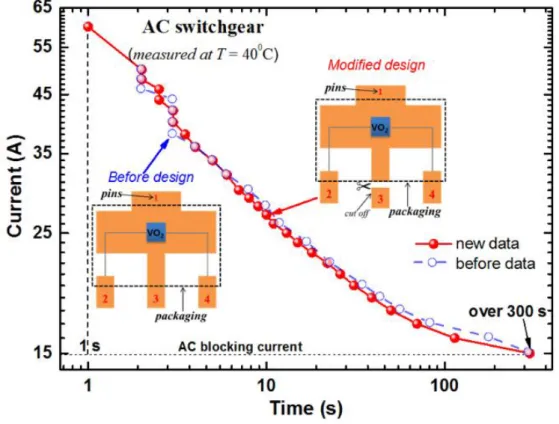
그림 3-2. CUT OFF TIME OF THE CURRENT OF THE AC SWITCHGEAR CONTROLLED BY TEMPERATURE OF THE CRITICAL TEMPERATURE SENSOR ··· 70
그림 3-3. MODIFICATION OF THE SWITCHGEAR PCB BY CHANGING A CAPACITANCE C AND A RESISTANCE R··· 71 그림 3-4. CUT OFF TIME OF THE CURRENT OF THE AC SWITCHGEAR CONTROLLED
BY TEMPERATURE OF THE CRITICAL TEMPERATURE SENSOR: RED CURVE CORRESPONDS TO DESIGN 1 WITH THE CTS (2) IN 그림 3-1; BLUE CURVE
CORRESPONDS TO DESIGN 2 WITH THE CTS (2)’ IN 그림 3-1; BLACK CURVE
CORRESPONDS TO MODIFIED PCB IN 그림 3-3. ··· 71
그림 3-5. MODIFICATION OF THE SWITCHGEAR BY THE SERIAL CONNECTION OF THE RESISTANCE TO THE CTS: R1=5.1 KΩ; R1=1.0 KΩ ··· 72
그림 3-6. CURRENT VS TIME MEASUREMENTS FOR TWO MIT SWITCHGEARS WITH THE RESISTANCE: (1) R1=5.1 KΩ; (2) R2=1.0 KΩ ··· 73
그림 3-7. MOTT TRANSITION REVEALED BY TEMPERATURE INDUCED RESISTANCE CHANGES IN A HIGH-QUALITY VO2 FILM ON SUPHIRE SUBSTRATE. RIGHT AND UPPER LEFT INSETS ARE DEPICTIONS OF THE LOW-TEMPERATURE MONOCLINIC M1 AND HIGH TEMPERATURE RUTILE TETRAGONAL R PHASES. BOTTOM LEFT INSET: HEXAGONAL STRUCTURE AND ORIENTATION OF DIFFERENT CUTS OF THE SUPHIRE. ··· 74
그림 3-8. SCHEMA OF THE PULSED LASER DEPOSITION (PLD) METHOD AND MODELING OF THE SURFACE MORTHOLOGY OF THE VO2 FILMS GROWN ON SUPHIRE SUBSTRATES WITH DIFFERENT CRYSTALLOGRAPHIC ORIENTATIONS AT LOW (5 MTORR, NON-STOICHIOMETRIC) AND HIGH (40 MTORR, STOICHIOMETRIC) OXYGEN PARTIAL PRESSURE ··· 75
그림 3-9. TEMPERATURE DYNAMICS OF THE RESISTANCE OF THE STOICHIOMETRIC (40 MTORR) AND NON-STOICHIMETRIC (5 MTORR) VO2 FILMS DEPOSITED ON R-, M- AND C-CUT SUPHIRE SUBSTRATE. CORRESPONDING TEMPERATURE DYNAMICS OF THE STRUCTURAL PHASE TRANSITION (M1 → R) OF THE STOICHIMMETRIC FILMS. ··· 76
그림 3-10. MIT CTS 를 활용한 과부하계전기 개념도. ··· 77
그림 3-11. MIT CTS 를 활용한 과부하계전기 회로도. ··· 78
그림 3-12. MIT CTS 를 활용한 과부하계전기. ··· 78
그림 3-14. 정전압 회로가 없는 회로. ··· 80 그림 3-15. 정전압 회로가 없는 회로 ··· 80 그림 3-16. MIT CTS 를 활용한 과부하계전기의 전류에 따른 차단시간. ··· 83 그림 3-17. 수정된 MIT CTS 를 활용한 과부하계전기 회로도. ··· 83 그림 3-18. 수정된 MIT CTS 를 활용한 과부하계전기 회로도. ··· 86 그림 3-19. 수정된 MIT CTS 를 활용한 과부하계전기 시험. (좌) MIT CTS 에 열을 가 지 않았을 때(우) MIT CTS 에 열을 가했을 때 ··· 87 그림 3-20. MIT CTS 를 활용한 교류 전자접촉기 제어 회로 ··· 87 그림 3-21. MIT CTS 를 활용한 교류 전자접촉기 제어 회로를 이용한 실험 ··· 88 그림 3-22. MIT CTS 와 PCB 보드 연결방법. (위) 병렬로 연결, (아래) SUS 를 통해 직 렬로 연결··· 88 그림 3-23. MIT CTS 와 PCB 보드 실제 연결방법. (좌) 병렬로 연결, (우) SUS 를 통해 직렬로 연결 ··· 90
그림 3-24. 발열도선 (A) CU, (B)CU, CU-P, CU, (C)CU, SUS, CU.··· 92
그림 3-25.(A) CU, (B)CU, CU-P, CU, (C)CU, SUS, CU 의 전류에 따른 온도 그래프. ·· 93 그림 3-26. (A) CU, (B)CU, CU-P, CU, (C)CU, SUS, CU 의 전류에 따른 온도 그래프. · 95 그림 4-1. V-ATOM POSITIONS IN DIFFERENT STRUCTURES OF VO2 FOR MOTT MIT
CONCEPTS. (A) MONOCLINIC INSULATING M1 STRUCTURE WITH THE CHARGE-DENSITY-WAVE (CDW) STRUCTURE FORMED BY TWISTED V-V
DIMERS WITH LATTICE DISTORTION RELATIVE TO CR (CR - V-V DISTANCE IN RUTILE PHASE); (B, D) MONOCLINIC INSULATING M2 STRUCTURE WITH TWO INTERSTRUCTURES: CDW S - THE CDW STRUCTURE FORMED BY UNTWISTED PAIRED V-ATOMS AND ICS – INSULATOR CHAIN STRUCTURE WITH AN EQUALLY SPACED TWISTED UNPAIRED V-CHAIN; (C) RUTILE OR PSEUDORUTILE (PR) TETRAGONAL METALLIC STRUCTURE WITH EQUALLY SPACED UNPAIRED UNTWISTED/TWISTED CHAINS OF V-ATOMS; (E) MONOCLINIC METAL MMP
(OR M3) STRUCTURE, IDENTICAL TO M2, WITH THE EQUALLY SPACED
TWISTED METALLIC V-CHAIN. THE IMT (OR MIT) OCCURS BETWEEN M2 AND MMP (OR M3) [12] WITHOUT STRUCTURAL DISTORTION. ··· 105 그림 4-2 (A) SCHEMATIC DIAGRAM OF THE MEASUREMENT SYSTEM. (B) RAMAN
IMAGE OF THE MONOCLINIC AG MODE OF 622 CM-1 FOR VO2. (C) PHOTOCURRENT IMAGE SIMULTANEOUSLY MEASURED AT 323 K (50C). (D) AFTER LASER ILLUMINATION, PHOTOCURRENT IMAGE WITH A
SCHOTTKY-NANOJUNCTION IMAGE AND, (E) RAMAN IMAGE OF THE
MONOCLINIC AG MODE OF 622 CM-1. (F) SCHOTTKY NANOJUNCTION IMAGE AND POSITIONS FOR MEASUREMENTS OF RAMAN SPECTRA. (G) RAMAN SPECTRA (A~H), MEASURED NEAR THE SCHOTTKY NANOJUNCTION,
DEMONSTRATING THAT THE STRUCTURE IS MONOCLINIC. (H) TEMPERATURE DEPENDENCE OF THE SCHOTTKY NANOJUNCTION IMAGES. ··· 108 그림 4-3. TEMPERATURE DEPENDENCE OF PHOTOCURRENT. THIS WAS MEASURED
FOR DEVICE I IN THE RAMAN-PHOTOCURRENT SYSTEM IN 그림 4-2(A). (A) AS TEMPERATURE INCREASES, RED AND BLUE IMAGES BECOME DARKER AND THEIR SIZE INCREASES. THE SCHOTTKY NANOJUNCTION IS DISPLAYED. (B) THE MAGNITUDE OF THE PHOTOCURRENT MEASURED AT THE LEFT SIDE OF THE IMAGE. SCHOTTKY PEAKS NEAR ELECTRODES AND SCHOTTKY
NANOJUNCTIONS (MAGNIFIED PEAKS SHOWN IN INSET) NEAR 16 M IN POSITION ARE PRESENTED. ··· 110 그림 4-4. (A) TEMPERATURE DEPENDENCE OF 1/PHOTOCURRENT IN 그림 4-3(B).
THE 1/PHOTOCURRENT CORRESPONDS TO RESISTANCE. THE ACTIVATION ENERGIES MEASURED AT LEFT AND RIGHT ELECTRODES ARE ACT LEFT ELECTRODE
77 MEV AND ACT RIGHT ELECTRODE 86 MEV. (B) TEMPERATURE DEPENDENCE OF
TSTRUCTURAL PHASE TRANSITION 341 K (68OC), THE MONOCLINIC PEAKS DISAPPEAR AND THE BROADNESS OF THE A1G PHONON MODE INDICATING
TETRAGONAL NEAR 520 CM-1 IS SHOWN. (C) AND (D), THE MAIN BAND
(D-BAND) FOR DIRECT TRANSITION AND AN EXTRINSIC SEMICONDUCTOR BAND FOR INDIRECT TRANSITION BEFORE AND AFTER THE IMT. UB – UPPER (ELECTRON) HUBBARD BAND (A1G(OR D11)+ BAND), LB – LOWER (HOLE)
HUBBARD BAND (A1G(OR D11) BAND) [38,39], EF – FERMI LEVEL, ΔDIRECT – ENERGY GAP FOR DIRECT TRANSITION (FOR VO2, 2ΔDIRECT 0.6 EV), ΔACT – ACTIVATION ENERGY FOR INDIRECT TRANSITION, Ω – THERMAL PHONON FREQUENCY, CB – CONDUCTION BAND. ··· 111 그림 4-5. (A) RESISTANCE (R) VS TEMPERATURE (T) CURVES FOR THE VO2 FILMS
WITH DIFFERENT THICKNESSES (S1 ≈ 130NM,S2 ≈ 90NM,ANDS3 ≈ 50NM), SYNTHESIZED ON ALN/SI(111). INSET IS THE GAUSSIAN FITTED DERIVATIVE OF THE LNR(T) FOR THE S1 SAMPLE WITH DETERMINED TC VALUES. THE SOLID AND OPEN CIRCLES REPRESENT THE TEMPERATURE RAMPING UP AND DOWN, RESPECTIVELY. AT THE BOTTOM FIGURE, GREY DOTTED LINES SEPARATE DIFFERENT REGIONS OF ELECTRICAL STATES OF VO2 (I: FULLY INSULATING; I + M: INSULATING + METALLIC, TRANSIENT REGION OF PHASE COEXISTENCE; M: FULLY METALLIC STATE ABOVE THE TAPP) AND THE ARROW BELOW THE BOTTOM FIGURE REPRESENTS PERCOLATION WITH INCREASING TEMPERATURE. (B) SEM IMAGES OF SURFACE MORPHOLOGY WITH
GRAIN-SIZE INDICATION (RED CIRCLE) OF THE VO2 FILMS WITH DIFFERENT THICKNESSES. (C) XPS SPECTRA OF THE VO2 FILM (AFTER 100 S OF
AR+-SPUTTERING) REVEALING THE V+4 VANADIUM OXIDATION STATE. ··· 119 그림 4-6.(A) Θ-2Θ XRD PATTERN OF THE VO2/ALN/SI HETEROSTRUCTURE. INSETS
(FWHM) OF THE VO2 (020) AND ALN (0002) PEAKS. (B) Φ-SCANS FROM THE
VO2 (011) AND ALN (101) PLANES. INSET SHOWS Φ-SCAN OF THE VO2 (220).
··· 123 그림 4-7. (A) HIGH-RESOLUTION TEM IMAGE OF THE VO2/ALN CROSS SECTION
WITH INSETS OF INTER-PLANAR SPACING ALONG VO2 [010] AND ALN [0001]
GROWTH DIRECTIONS. (B) AND (C) SELECTED-AREA-ELECTRON-DIFFRACTION PATTERNS OF VO2 AND ALN, RESPECTIVELY, OBTAINED FROM (A). (D)
SCHEMATIC GROWTH STAGES OF THE VO2 FILM ON ALN: BLUE BALLS— AL
ATOMS POSITIONED AT DISTANCE IALN FROM EACH OTHER; BLUE-RED
BALLS— V AND AL ATOMS FORMING INTERFACE REGION WITH
THICKNESS TC THAT APPEARS AT THE INITIAL STAGE OF THIN FILM GROWTH
HAVING A DISTORTED VO2 STRUCTURE; RED BALLS— V ATOMS POSITIONED
AT DISTANCE IVO2 FROM EACH OTHER FORMING THE VO2 FILM WITH
THICKNESS TVO2. (E) SCHEMATIC TOP VIEW OF ALIGNMENT OF
VO2 (IN-PLANE DIRECTIONS: [100] FOR AVO2, [001] FOR CVO2 WITH ANGLE Β
= 122.6° BETWEEN THEM, AND [101] FOR DIAGONAL; OUT-OF-PLANE DIRECTION: [010] FOR BVO2) ON ALN (IN-PLANE
DIRECTIONS: [21̄ 1̄ 0][21̄1̄0] FOR AALN, [1̄ 21̄ 0][1̄21̄0] FOR BALN WIT
H ANGLE Γ = 120.0° BETWEEN THEM, AND A SHORT
DIAGONAL D DIRECTION OF THE TWO ALN CELLS; OUT-OF-PLANE
DIRECTION: [0001] FOR CALN). (F) SCHEMATIC ARRANGEMENT (TOP VIEW) OF
V-ATOMS (RED BALLS) IN THE VO2 FILM ON AL-ATOMS (BLUE BALLS) IN THE
ALN LAYER HAVING HEXAGONAL DOMAINS (BLUE LINES); VO2 UNIT CELL
(RED AND PINK DASHED LINES) SYMMETRICALLY ROTATED FOR 60° IN A COUNTER-CLOCKWISE DIRECTION AROUND ITS OUT-OF-PLANE B-AXIS FORMING QUASI-HEXAGONAL VO2 STRUCTURE. (G) MODELING OF THE
VO2/ALN CROSS SECTION WITH [101] ZONE AXIS OF
VO2 AND [21̄ 1̄ 0][21̄1̄0] ZONE AXIS OF ALN OBTAINED FROM (A), (B),
AND (C). ··· 125 그림 4-8. SCHEMATIC DIAGRAM SHOWING DEFORMATION OF THE VO2 FILM
STRUCTURE WITH RESPECT TO THE BULK SINGLE CRYSTAL: THE OUT-OF-PLANE B-AXIS HAS THE COMPRESSIVE STRAIN AND THE BASE A-C PLANE HAS THE TENSILE STRAIN WITH A- AND C-AXES
EXTENSIONS. INSET DISPLAYS THE TILTED DIMERS OF THE M1 PHASE FOR A
BULK SINGLE CRYSTAL AND THE FILM. AS A RESULT OF THE STRAINS, THE DISTANCE, LB, BETWEEN V4+ AND V4+ IONS FOR THE BULK SINGLE CRYSTAL IS SMALLER THAN LF FOR THE THIN FILM. RIGHT TABLE SHOWS THE LATTICE PARAMETERS (A, B, AND C), WITHOUT CONSIDERING EXPERIMENTAL ERRORS, THE BASE PLANE AREA (A × C) OF THE BULK SINGLE CRYSTAL AND OUR THIN FILM. ··· 126 그림 4-9. SHOWS DESIGN OF THE PATTERNS WITH VARIOUS SHAPE AND SPACING BETWEEN ETCHED (WHITE) AND UNETCHED (BLACK) REGIONS. ··· 128 그림 4-10.SEM IMAGES OF THE AU/TIO2 PATTERNED SURFACE··· 129 그림 4-11.PATTERN IMAGE: INITIAL, AFM AND TEMPERATURE DEPENDENT
NEAR-FIELD ··· 130 그림 4-12. PATTERN IMAGE: INITIAL, AFM AND TEMPERATURE DEPENDENT
NEAR-FIELD ··· 131 그림 4-13. PATTERN IMAGE: INITIAL, AFM AND TEMPERATURE DEPENDENT
NEAR-FIELD ··· 132 그림 4-14. THE UNIT CELLS FOR M1, M2 AND R PHASES OF VO2. KEY DIFFERENCE
BETWEEN M1 AND M2 PHASES IS AN ARRANGEMENT OF V ATOMS ALONG THE RUTILE CR-AXIS. ··· 133
그림 4-15.DROP IN RESISTANCE FOR 120 NM VO2 FILM ON ALN/SI ··· 134 그림 4-16. TRUCTURAL CHARACTERIZATION OF VO2/ALN. (A) HRTEM IMAGE OF
THE VO2/ALN CROSS-SECTION WITH TWO FFT PATTERNS FROM DIFFERENT VO2 STRUCTURES M1 AND M2 (WHITE DASHED SQUARES) OBSERVED AT ROOM TEMPERATURE. (B, C) MAGNIFIED WHITE-DASHED AREA OF M1 AND M2 TAKEN FROM (A) AND MODELED STRUCTURES ALONG [010]M1 GROWTH DIRECTION AND [100]M1 ZONE AXIS FOR M1-VO2 AND [001]M2 GROWTH DIRECTION AND [110]M2 ZONE AXIS FOR M2-VO2. (D) EPITAXIAL ALIGNMENT OF THE M1 AND M2 PHASES OF THE VO2 FILM ON THE ALN LAYER. ··· 136 그림 4-17. TEMPERATURE DEPENDENCE OF THE RESISTANCE OF VO2/TIO2 AND
VO2/AL2O3 SAMPLES ··· 137 그림 4-18.SURFACE MORPHOLOGY CHARACTERIZATION OF VO2/TIO2: SEM (A)
AND AFM (B) IMAGES ··· 138 그림 4-19. TEMPERATURE DEPENDENT XRD REVEALED M1 → R STRUCTURAL
PHASE TRANSITION IN VO2/TIO2··· 139 그림 4-20. 열동형 과부하계전기 TOR-AC220V-BD-V3.0 의 회로도. ··· 140 그림 4-21.TOR-AC220V-BD-V.3.0. ··· 141 그림 4-22. SCR 제어 회로 비교. (위) MOSFET 을 사용한 경우, (아래) MOSFET 을 사 용하지 않은 경우. ··· 142 그림 4-23. TOR-AC220V-BD-V4.0 회로도. ··· 144 그림 4-24. TOR-AC220V-BD-V5.0 회로도 ··· 145 그림 4-25.TOR-AC220V-BD-V5.0 회로의 문제가 되는 부분. ··· 146 그림 4-26. TOR-AC220V-BD-V6.0 회로도 ··· 147 그림 4-27. TOR-AC220V-BD-V7.0 ··· 148 그림 4-28. TOR-AC220V-BD-V7.0 시뮬레이션에 사용된 회로. ··· 148 그림 4-29. CTS 가 동작하였을 때 MOC 3022 에 흐르는 전류(SIMULATION)(주위 온
도에 따라 붉은색: 20 도, 하늘색: 25 도, 자주색: 30 도, 회색: 35 도, 초록색: 40 도). ··· 149 그림 4-30. 실제 제작된 TOR-AC220V-BD-V7.0 의 모습 ··· 149 그림 4-31. TOR-AC220V-BD-V7.0 사진. ··· 150 그림 4-32. 전자개폐기의 전류에 따른 차단시간. ··· 150 그림 4-33. HTR 을 이용한 LED 제어 회로도. ··· 152 그림 4-34. R2 크기에 따른 LED 에 흐르는 전류 그래프. (위) 10KOHM (중 간)50KOHM(아래)100KOHM ··· 153 그림 4-35. R3 에 병렬로 CAPACITOR C1 을 연결한 회로도. ··· 154 그림 4-36. C1 에 0.01UF CAPACITOR 를 연결한 모습. ··· 154 그림 4-37. LED 입력단에 흐르는 전류 및 R3 에 걸리는 전압 그래프. ··· 155 그림 4-38. 인덕터 L1 을 추가적으로 부착한 회로. ··· 155 그림 4-39. INDUCTOR 를 부착하였을 때 그래프. ··· 156 그림 4-40. 플리커 측정을 위한 실험 구성. ··· 157 그림 4-41. V2O5 로 측정한 RAW DATA ··· 158 그림 4-42. 제작한 LED 등의 LIGHT INTENSITY 변화. ··· 158 그림 4-43. LIGHT INTENSITY 의 FFT 결과. 약 60KHZ 로 진동하고 있다. ··· 159 그림 4-44. 다양한 안정기들에 대한 측정 결과. ··· 160 그림 4-45. LED 형광등 연결도 및 측정결과 ··· 162 그림 4-46. LED 플리커 현상 측정 결과. ··· 162 그림 4-47. LED 형광등 광효율 측정 결과. ··· 163 그림 4-48. CIRCUIT DIAGRAM ··· 163 그림 4-49. 모터(R1)에 흐르는 전류. ··· 164 그림 4-50. 모터에 전류가 들어가기 시작하는 상황. 처음 전류가 들어갈때 모터의 저항은 낮은 상태이고 이후 모터가 돌게 되면서 저항이 늘어나게 된다. ··· 165 그림 4-51. 모터가 정지해 있다가 회전하기 시작하는 경우에 모터에 흐르는 전류.
··· 166 그림 4-52. 다이오드 레지스터 구조 ··· 166 그림 4-53. MIT 소자 위치에 고정저항을 교체하여 보호기능 없이 레지스터 대체용 으로 만들어진 모듈. 다이오드 발열을 측정하기 위해 THERMOCOUPLE 을 방열 판 뒷쪽에 부착.그림 4-53 는 시험에 사용된 다이오드 레지스터 모습이다. 그림 4-53 을 보면 다이오드 발열 측정을 위해 THERMOCOUPLE 을 방열판 뒤쪽에 부착하여 다이오드의 온도를 측정하였다. 그림 4-53 에서 붉은색으로 표시된 부분은 사용하지 않는 회로이다. ··· 167 그림 4-54. 환경 온도 120 도에서 다이오드 레지스터 시험 결과.··· 168 그림 4-55. 전압변동 테스트. ··· 169 그림 4-56. 85 도 설정후 내구시험결과 ··· 170
제 1 장 ETRI 주요 사업, 금속-절연체 전이(Metal-Insulator
Transition:MIT) 현상규명 및 응용기술 개발 과제
제1절 사업 개요
ETRI 창의연구실사업은 2012 년부터 2015 년까지 5 년간 수행되는 정부출연금 사업 으로서, 2016 년부터 주요사업으로 변경되면서 그 사업속에서 “금속-절연체 전이 현상규명 및 응용기술 개발” 이라는 세부과제로 연구가 수행되었다.제2절 사업 목표 및 내용
○ 최종연구목표 금속-전연체전이(MIT) 현상규명 및 MIT 신재료, 스위치 및 응용기술 개발 ○ 목표금속-절연체 전이(Metal-Insulator Transition, MIT) 현상규명 및 MIT 나노기초 핵심응용 기술 개발을 통한 강상관 물질에서 MIT 현상을 연구하고, 핵심 응용소자 로써 MIT 센서, 스위치, 파워 소자 등을 개발한다. 그리고 개발 된 응용소자를 이 용하여 관련 응용 기술 개발을 수행한다. 또한 MIT 현상과 응용에 대한 국제공동연 구를 수행함으로써 MIT 의 학문적 기초와 응용 기술을 더욱 깊이 있게 발전시키고 자 한다.
MIT 현상규명을 위하여 MIT 물질 VO2 에서 코히런트 포논의 온도의존성을 조사하 여 M2 구조에서 구조 상전이를 겪지 않는 MIT 현상을 최초로 관측한다. 또 나노 레 벨급 광전도도와 라만산란 실험을 동시에 관측하여 구조상전이 없는 MIT 를 관측한 다. 그리고 국제공동연구로서 나노레벨에서 팸토초 기술로 MIT 현상을 측정하였다. MIT 의 대표적인 강상관 물질인 VO2 를 Pulsed Laser Deposition(PLD) 방법으로 산
소분압을 조절하여 박막을 제조하여 그 박막의 특성을 저항의 온도의존성, SEM 과 XRD 등의 물성 분석을 통해 임계특성의 변화를 관측조사 한다. 그 박막의 대량생산 을 위하여 Si 기판 위에 VO2 Epi 박막을 제조한가.
MIT Critical Temperature Switch(CTS)를 이용하여 MIT 전자개페기와 차단기, MIT CTS 와 NDR 스위칭을 LED 발광에 적용하여 MIT-NDR 현상을 이용하는 램프를 발명하 였다. 자동차 라디에이터 팬모터의 과전류 방지를 위하여 다이오드 레지스터를 새 롭게 발명한다.
제3절 사업 수행 체계
최종목표: 금속-전연체전이(MIT) 현상규명 및 MIT 신재료, 스위치 및 응용기술 개 발 그림 1-1. 연구 수행 체계제4절 보고서 체계
본 보고서는 1 장에서 주요 사업, 금속-절연체 전이(Metal-Insulator Transition:MIT) 현상규명 및 응용기술 개발 과제에 대한 전반적인 내용에 대하여 기술며, 2 장에서는 2014 년 금속-절연체 전이 현상규명 및 응용기술 개발 과제의 연구목표 및 연구결과를 기술하며, 3 장에서는 2015 년 금속-절연체 전이 현상규명 및 응용기술 개발 과제의 연구목표 및 연구결과에 대하여 기술한다. 또한 제 4 장 에서는 2016 년 금속-절연체 전이 현상규명 및 응용기술 개발 과제의 연구목표 및 연구결과에 대하여 기술하며, 5 장에서는 과제의 성과를 종합하며, 향후 발전을 위 한 건의사항을 제안한다.제 2 장 2014년 금속-절연체 전이 현상규명 및 응용기술 개발
제1절 연구목표
1. EFFECT OF OXYGEN PARTIAL PRESSURE ON THE PROPERTIES OF VO
2FILMS
GROWN BY PULSED LASER DEPOSITION METHOD
It is known that metal-insulator transition (MIT) in Vanadium Dioxide (VO2)
is accompanied by “jump” in the resistivity of several orders of magnitude. Because of the remarkable properties, this “smart” material had become very attractive for technological applications (sensors, switches, transistors etc.). To take all advantages of the huge potential of VO2, it is necessary to fully
understand its properties and their dependence on different conditions. In particular, for getting high-quality VO2 thin films, the most crucial is their
fabrication process. For this reason, we have investigated the MIT properties of nanosized VO2 films, as well as their surface morphology, composition and
structure, depending on deposition conditions, specifically, oxygen partial pressure maintained during films growth.
2. MODIFICATION OF METAL-INSULATOR TRANSITION IN VO
2FILMS GROWN ON
TIO
2SUBSTRATES
It is known that at normal conditions, critical temperature of the MIT (TMIT)
in VO2 is ~340 K. Therefore, its decreasing to room temperature values is “hot
for the latter are interfacial strain engineering and growth parameters modification. For this reason we have studied the properties of VO2 thin films
grown on TiO2 substrates with different lattice constants (induced different
strain) and influence of deposition conditions on them.
3. THERMOPOWER SWITCHING IN METAL-INSULATOR TRANSITION MATERIALS
Nowadays, scientific and industrial interest in effective and ecological energy usage is especially intensified. Vital importance has question about renewability, conservation and conversion of energy. One of the perspective solution routes is based on direct electrical energy generation from heat. This phenomenon is known as thermoelectric effect, discovered by T.J. Seebeck in 1821. It emerges when a temperature gradient ( ) exist between two different conducting materials, which leads to charge carriers diffusion and redistribution, and, thus, to arising of electrostatic potential difference ( ).
It is known, that good thermoelectric material should have high thermoelectric power (or Seebeck coefficient ) to maximize heat conversion to electricity, high electrical conductivity to minimize losses for Joule heating, and low thermal conductivity to prevent thermal shorting. However, according to Wiedemann-Franz law: ,(where and are thermal and electrical conductivity, respectively, is temperature), these conditions are controversial and cannot be simultaneously fulfilled. New materials with controllable crystal and electronic structure are required. An opportunity for carrier concentration regulation can provide the strongly correlated electronic materials. In the later, an active manipulation of electrons charge and spin degrees of freedom, and the atomic orbital orientations would create the
electronic structure and charge carrier-related properties required for high-performance thermoelectric materials.
On the example of Vanadium Dioxide, regarded as a model strongly correlated material, we have studied the thermoelectric power switching in the temperature range 300-400 K and possibility of its enhancement due to fabrication of heterostructure, composed of VO2 thin film and highly-doped silicon substrate.
4. 솔-겔 법으로 성장된 V
1-xW
xO
2(0≤x≤4.0 at.%)박막에서의 텅스텐
불순물이 미치는 영향과 그 전기적 구조적 특성 및 소자제작
금속-절연체 전이현상이 관측 된 물질가운데 가장 잘 알려진 VO2박막은 340K 부근 에서 급격한 전이현상을 일으킨다. 본 연구 그룹에서는 이 전이현상을 이용하여 열 전 센서 및 임계 온도 스위치로의 응용소자 및 소자를 이용한 어플리케이션 개발 을 위해 연구 중이다. 이에 따라 전이온도를 적정 소자 요구조건에 맞게 가변 시킬 수 있다면, 소자로서의 응용과 활용 범위가 더욱 넓어 질 수 있을 것이다. MIT 창의연구센터에서는 소자의 전이온도를 가변 시키기 위하여 VO2 박막에 금속이 온을 첨가하는 연구가 진행되어왔으며 특히 W6+, Mo6+, Ta5+, Cr3+, Al3+, Fe3+ 등의 금 속이온을 불순물로서 첨가하면 전이특성이 변화한다는 것을 확인할 수 있었다.제2절 연구내용
1. EFFECT OF OXYGEN PARTIAL PRESSURE ON THE PROPERTIES OF VO
2FILMS
GROWN BY PULSED LASER DEPOSITION METHOD
orientations ), ), ) and ) or r-, a-, c- and m-plane, respectively) by pulsed laser deposition (PLD) method. A KrF excimer laser with a radiation wavelength of 248 nm was used to ablate the metallic vanadium target. The energy of the laser pulse was 300 mJ and the pulse repetition rate was set at 10 Hz. Prior to deposition, the chamber was evacuated to ~10− 6 Torr and oxygen
gas was introduced into it for reactive deposition. During thin film growth, the O2 partial pressure (P(O2)) was maintained in the range 5-40 mTorr and substrate
temperature 7000C. Films thickness was about 80 nm.
Results and discussion. 그림 2-1 shows temperature dependence of the electrical properties of VO2 films grown on sapphire substrates at different oxygen partial
pressure. Resistance of the films was measured by four-probe method in a cryostat system in the temperature range 300-380 K on heating and cooling (with rate 2 K/min) to study hysteresis behavior. The main MIT characteristics of the films were defined as followings: Transition temperature TMIT: peak position in the derivative curve of the resistance as a function of temperature; The ratio (amplitude) of the resistance “jump” ΔR: the ratio of the film resistance measured at 300K and 380 K, i.e. ΔR=R(300K)/R(380K); Sharpness of the MIT ΔS: full width at half maximum (FWHM) of the derivative curves; Thermal hysteresis width ΔT: difference between transition temperature of heating (TMIT↑) and cooling curve (TMIT↓).
그림 2-1. Temperature dependencies of the resistance, normalized resistance (upper inset) and corresponding derivative curve (lower inset, only for best quality samples ~40 mTorr) of the resistance for VO2 films deposited on (a) r-,
(b) a-, (c) m- and (d) c-plane sapphire substrates at different oxygen partial pressure. The solid and open circles represent temperature ramping up and down, respectively.
General phase transition characteristics (defined from the resistance curves) of VO2 films grown on sapphire substrates with different orientation are depicted in the 그림 2-2.
그림 2-2. Phase transition characteristics of VO2/Al2O3 samples
From the above data 그림 2-2it is shown: film resistance and value of its changes during MIT (RMIT), transition temperature (TMIT) and sharpness of the transition (defined by FWHM), and width of thermal hysteresis (ΔTMIT) strongly depend on oxygen partial pressure, that is maintained during thin film fabrication process, as well as on substrate orientation; increasing O2 pressure, the resistance of
the films in the semiconductor phase (before MIT) increase, while in metallic state its value is almost the same for all O2 pressures (except VO2/c-Al2O3) →
it is possible to obtain incredible big “jump” in the films resistance; varying O2 pressure (creating oxygen deficient or excess films) we can modify ΔTMIT and FWHM and, thus, get appropriate films for technological application (sensors,
optical memory etc.). Surface morphology and thickness of the films were investigated by scanning electron microscopy (SEM) (그림 2-3).
그림 2-3. SEM images of the surface morphology of VO2 films on Al2O3 substrates grown at different oxygen partial pressure
From SEM images (그림 2-3) it can be seen that with increasing oxygen partial pressure, the surface of the samples becomes smoother with well-developed grains, size and shape of which are varying with substrates and deposition conditions. It should be noted, that in case of VO2/c-Al2O3 at ~40mTorr, small voids between
grains starting to appear. Further rising of oxygen pressure will lead to increasing of the voids size and roughness. The same behavior, at P(O2)>40mTorr,
also can be observed for the films deposited on the substrates with another orientations (not shown here). This effect may restrict the percolation of the
current and, thus, significantly increase the film resistance. Thereby, we can conclude that increasing the oxygen partial pressure (until certain value, exceeding which, the intergrain voids appear) results in the rising of the grain size and enhancement of the surface flatness. Due to these, the grain boundaries are reduced and, thus, transition properties become better.
In order to find out the oxidation state of vanadium and its changes with oxygen pressure, X-ray photoelectron spectroscopy of the VO2 films, deposited at high P(O2) (i.e. films with the biggest value of “jump”) on sapphire substrates with
different orientation (그림 2-4a) and VO2 films on m-plane Al2O3, deposited at
different oxygen pressure (그림 2-4b) were measured.
그림 2-4. XPS spectra (after 100s Ar+-sputtering) of VO2/Al2O3 deposited at high oxygen pressure on substrates with different orientations (a); at different oxygen pressure on m-plane Al2O3 (b)
Details of the fitting of the V2p and O1s XPS signals are given in 표 2-1. As can be seen from 그림 2-4a and Table 1, in case of the films deposited at high P(O2) (35-40 mTorr), BE for the V2p3/2 and O1s peaks is approximately 516 eV
and 530 eV, respectively, with difference Δ≈ 14eV. These results are in good agreement with before published data and confirm that oxidation state of vanadium in our films is V+4. Note, that in case of VO
inhomogeneity obtained from SEM data, XPS spectrum was measure on the sample deposited at lower, but still high, oxygen pressure ~35 mTorr. For this reason the BE for V and O peaks for this sample is slightly shifted to smaller values compare with other samples in 그림 2-4a.
Sample
E
(V2p3/2),
eV
FWHM
(V2p3/2),
eV
E (O1s), eV
FWHM
(O1s), eV
Δ, eV
a_40 516.0 4.26 530.1 2.19 14 c_35 515.9 4.17 529.95 2.17 14.05 m_40 516.2 4.22 530.05 2.16 13.85 m_20 516.2 4.30 530.15 2.21 13.95 m_5 515.9 4.36 529.9 2.16 13.95표 2-1. XPS fit parameters for V2p and O1s peaks of VO2 films on Al2O3 substrates
Δ – binding energy (BE) difference: Δ= E (O1s) - E (V2p3/2).
To found out the influence of the oxygen partial pressure on the BE, we have measured the XPS of the films, deposited on m-plane Al2O3 at various P(O2). From
그림 2-4b can be seen, that while oxygen pressure decrease from 40 to 20 mTorr, the peaks for V2p3/2and O1s become broader, resulting in FWHM increase from 4.22 (at 40mTorr) to 4.30eV (at 20 mTorr) for V2p3/2, and from 2.16 (at 40mTorr) to 2.21 (at 20 mTorr) for O1s. When P(O2)=5mTorr, the binding energy of these peaks
shifts to smaller values for 0.3eV (see Table 1). This lowering of BE for the V2p3/2 and peak broadening indicate the reduction of the V+4 oxidation state,
because of the oxygen vacancy formation. The later results in the resistance drop in the semiconductor phase and suppression of the MIT.
films grown on r-, a-, c- and m-plane sapphire substrate at high and low oxygen pressures. Crystalline structure of the thin films was determined by X-ray diffractometer (Rigaku D/MAX 2500) using Cu Kα with diffraction angle scanning range 100-900 .
그림 2-5. XRD patterns of VO2 films deposited on sapphire with different orientations, at high and low oxygen partial pressure
In particular, for rich-oxygen VO2 on r-Al2O3 we can observe strong peak at 36.5
º, which can be (200) or/and (-211), due to their close Brag angles, and weak (111) peak. For VO2 on c-Al2O3 the well-resolved peaks are located around 2θ
~40º and ~86º, that can be ambiguous (because of their similar d-spacing) indexed as monoclinic (020)/(002) and (040)/(004), respectively. For these samples also we can observe two extra peaks: one at ~20.5º that can be (010)
peak and another one at ~64.5º, which can be classified as (203) or (040) according to JCPDS cards. In case of VO2 on a-plane sapphire we can see peaks
corresponding to (100) orientation and (-402). For VO2/m-Al2O3 deposited at high
partial pressure, (203) peak can be observed and for those, deposited at low P(O2),
additional peak at ~33.6º appears, attributed as (310) peak.
In general, from XRD patterns it can be seen that in case of films deposited at low partial pressure, the peaks are broader with lower intensity, compare with films grown at high pressure, besides they are shifted to higher 2θ values, resulting from compression of b-lattice parameters due to oxygen vacancies incorporation.
Conclusions. Thus, it can be seen, that magnitude and behavior of the MIT strongly depend on oxygen partial pressure that is maintained during thin film fabrication process and also from substrate crystallographic orientation. Specifically, increasing P(O2), stoichiometric VO2 films can be obtained (that
was proved by XPS data) that leads to the reduction of density of point defects, like interstitial vanadium atoms and oxygen vacancies, as well as their complexes, resulting in enhancement of films structure and MIT speed. Also, as was confirmed by SEM data, with increasing P(O2), grain size of the films is enlarged, that
reduces harmful boundary effect on the MIT.
2. MODIFICATION OF METAL-INSULATOR TRANSITION IN VO
2FILMS GROWN ON
TIO
2SUBSTRATES
VO2 thin films were grown on TiO2 (001) and (110) substrates by PLD method in
oxygen atmosphere with deposition rate of about 0.5 nm/min. For comparison, films were also deposited on sapphire substrates.
The influence of the oxygen partial pressure, substrate temperature and growing time on the electrical properties of the films were investigated by four-probe method. Samples morphology was investigated by scanning electron microscopy (SEM), crystalline structure and its changes with temperature - by X-ray diffractometer (Rigaku D/MAX 2500) using Cu Kα.
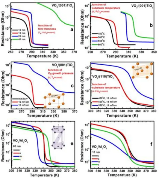
Results and discussion. In 그림 2-6 the resistance of VO2 films on (001) and
(110) TiO2, and VO2 films on r-, a-, c- and m-Al2O3 substrates are presented as
a function of temperature.
Corresponding derivative curves of the resistance temperature dependences of VO2 films on TiO2 and Al2O3 substrates are shown in 그림 2-7. From the Fig. 그
림 2-6 data it can be seen that properties of VO2 films in dependence of interfacial strain (caused by film substrate lattice mismatch) and deposition conditions provided by PLD method shown the following tendency: the MIT critical temperature can be shifted to near RT values and modificated up to 60 K for the VO2 films on TiO2 substrates with different crystallographic orientations. the TMIT changes for VO2/Al2O3 substrates are relatively small – up to 15 K. SEM image of VO2 thin films on (001) and (110) TiO2 substrates are shown on the
그림 2-6. Resistance vs temperature of the of VO2 films deposited on different substrates in dependence on: films thickness d (substrate: TiO2 (001)) (a), substrate temperature Ts (substrate: TiO2 (001)) (b), oxygen growth pressure P(O2) (substrate: TiO2 (001)) (c), substrate temperature Ts (substrate: TiO2 (110)) (d), substrate orientations for film thickness 80 nm (substrate: Al2O3) (e), substrate orientations for film thickness 80 nm (substrate: Al2O3) (f)
그림 2-7. Derivative curves of the resistance vs. temperature for VO2/TiO2 and VO2/Al2O3 demonstrating shift of the transition temperature TMIT
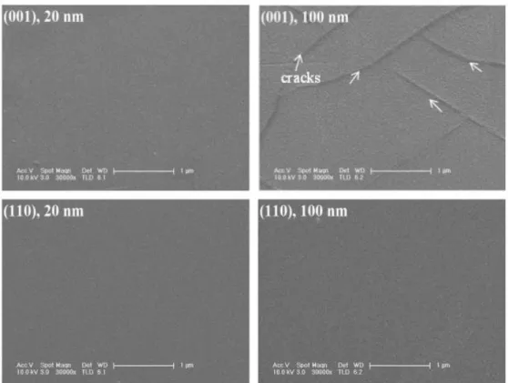
그림 2-8. SEM image of surface morphology of 20 and 100nm of VO2 thin films deposited on (001) and (110) TiO2 substrates
SEM demonstrates the high-quality of the films with smooth, densely-packed grains. In case of thick films (~100nm) on TiO2 (001) the cracks due to strain
relaxation can be observed. As a result of this relaxation, the transition temperature shifts to higher value compare with those one observed for ultrathin films.
Crystalline structure patterns of the films are depicted in Fig. XRD data confirms that VO2/TiO2 are highly-oriented single-phase epitaxial films.
그림 2-9. XRD patterns of the VO2 film deposited on (001) and (110) TiO2 substrates
In order to in-situ investigate structural phase transition, temperature dependence of the X-ray diffraction was measured with step 3 K (그림 2-9). Thus, the structural changes from rutile metallic R phase, corresponding to XRD (002)R
peak at 297 and 293 K, to monoclinic insulating M1 phase, corresponding to XRD
(-402)M1 peak at 291 and 288 K, can be observed. Note, that there existence of
그림 2-10. XRD (T) patterns of the VO2/(001)TiO2 substrates
Conclusions. It was shown that through engineering of the film-substrate interfacial strain, the critical temperature of the metal-insulator transition can be tuned and shifted to the room temperature values, that increase and broaden the practical application of the films.
3. THERMOPOWER SWITCHING IN METAL-INSULATOR TRANSITION MATERIALS
Vanadium dioxide (VO2) is canonical strongly correlated material undergoing
a first-order metal-insulator transition (MIT), accompanied by abrupt and reversible changes in electrical and optical properties. In particular, the “jump” in the electrical resistivity can reach five orders of magnitude at critical temperature TMIT≈ 340 K (그림 2-11). Along MIT in VO2 the structural
changes from a low-temperature monoclinic insulating M1 to high-temperature
rutile tetragonal metallic R phase takes place (insets in 그림 2-11). During structural transition, the V-cations that in R-phase (at T>TMIT, see right inset
on 그림 2-11) are positioned along CR-axis (or [001]R) at equal distances of
CR≈ 2.87Å between each other, become tilted and shifted for Δ (at T<TMIT, see
left inset on 그림 2-11), forming alternative long and short interspacing (charge density wave), equal 3.12Å and 2.65Å, respectively. Wherein, neighboring V-V cations form stable pairs or dimers, responsible for strong electron correlations.
However, the transition properties of nanosized films (like MIT amplitude and its sharpness, critical temperature and hysteresis width) and their structural peculiarities strongly depends on the films growing method and its conditions, as well as substrate type.
For thermoelectric measurements, VO2 films were grown on highly-doped p- and n-type (100) Si substrates by pulsed laser deposition (PLD) method, using 248 nm KrF excimer laser for a metallic vanadium target ablation. Thin films were deposited in oxygen atmosphere with partial pressure 10 mTorr. Substrate temperature was maintained at 7000C. Thickness of the films was about 150 nm.
그림 2-11. Temperature driven metal-insulator transition in VO2 and schematic
description of structural phase transition (insets) with changing V-cations position from monoclinic insulating M1 to tetragonal metallic R phase. CR~2.87
Å - V-V distance in R structure, Δ – lattice distortion (charge-density wave) and V-V dimerization during R→M1 transition.
Surface morphology of VO2/Si samples, obtained by scanning electron microscopy
(SEM), is depicted on 그림 2-12. SEM images show that VO2 films on p- and n-Si
have similar morphology characterized by rough, densely-packed grains with size 50-150 nm.
Crystalline structure of the films was determined by X-ray diffractometer (Rigaku D/MAX 2500) using Cu Kα with diffraction angle scanning range 100-900 (그림 2-13).
On XRD spectra multiple peaks appear due to different crystallographic orientation of film crystals.
그림 2-12. SEM image of the surface morphology of VO2 films on p- and n-type Si substrates
그림 2-13. XRD patterns of VO2 films deposited on p- and n-type Si substrates
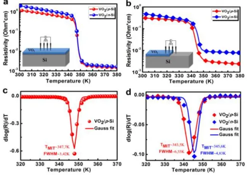
In order to characterize the MIT properties of the films, temperature dependencies of the resistivity (Fig. 4-14) were measure by four-probe method in the temperature range 300-380 K with heating rate 2 K/min. The measurements were performed in two geometries: lateral (Fig. 4-14a) and vertical (Fig. 4-14b). As for Si-substrate, so its resistivity changes with temperature demonstrates expectable metallic behavior (not shown here), as samples were highly-doped. Thus, according to the company-producer specification on silicon wafers, its resistivity is: 0.001 ~ 0.005 Ωcm for p-Si, which corresponds to the B-dopant density n = 1.7×10²⁰~2.0×1019 cm-3 and 0.01 Ωcm for n-Si → n = 4.53×1018 cm-3
of P-dopants.
Temperature of the metal-insulator transition was determined as the peak position of derivative curves of the resistivity vs. temperature (Fig. 4-14c,
d). It can be seen (Fig. 4-14c) that the TMIT in the lateral case is same for VO2/p-Si
and VO2/n-Si and is approximately equal 347.7 K. However, in case of vertical
measurement, TMIT is lower and equal 343.5 K and 345.6 K for VO2/p-Si and VO2/n-Si
samples, respectively. This difference can be caused by substrate effect on the film properties. Thus, from Hall-effect data, it is known that VO2 has n-type
conductivity, and when it is deposited on p-type Si substrate, a p-n junction is formed on the film-substrate boundary, that can be the reason of transition temperature reduction.
그림 2-14. Temperature dependence of the resistivity of VO2 films on highly-doped p- and n-type Si substrates measured in lateral (a) and vertical (b) cases; corresponding derivative curves for VO2/p-Si (c) and VO2/n-Si (d)
Theoretical and experimental description, results and discussion: Thermopower measurements
It is known that Vanadium Dioxide has negative Seebeck coefficient S, because electrons are its dominant charge carriers. Usually, the value of VO2 thermopower
in semiconductor phase can be varied from -20 to -1000 μV/K, depending on samples stoichiometry and quality. While in the metallic state the S value is approximately equal -25 μV/K (without significant fluctuations) with slight rising with temperature. And the absolute value of Seebeck coefficient of highly-doped Si is found to be in the wide range of μV/K (from hundred to several hundreds), depending on its doping level and it is weakly increases with temperature. Integrated thermoelectric properties of the VO2/Si heterostructure
are shown and discussed below.
Investigations of thermopower or Seebeck coefficient of VO2 films on highly-doped
Si were conducted on self-developed setup of Physical Properties Measurement System (PPMS). The samples were measured in temperature range 300-400K in lateral (그림 2-15a) and vertical (그림 2-15b) directions, and laterally on bare Si substrate (그림 2-15c) as well. Temperature gradient between hot and cold ends was ~10K with sample size (5x3) mm2. Obtained results are shown on 그림 2-15d,e. From the below figures, it can be seen that the thermopower of bare silicon substrate changes monotonically with temperature, slightly increases with heating. As for thermopower of heterostructures, so its value undergoes “MIT” and its sign depends on the substrate doping type: (in case of VO2/p-Si it has
positive sign, and in case of VO2/n-Si – negative). Before MIT, the S is the
integrated value of thermopowers on VO2 and Si. Note, that value of the S of
VO2/n-Si sample is much higher than VO2/p-Si (however, actual VO2 thermopower on p-Si is much higher than on n-Si), that can be caused by different doping level
그림 2-15. Scheme of thermopower measurements: lateral (a) and vertical (b) geometry for VO2/Si, lateral (c) for Si. Temperature dependence of thermopower
of VO2 films on p- (d) and n-type (e) silicon substrates, and just silicon substrate.
of the Si substrate. In particular, the maximum thermopower measured laterally on VO2/n-Si is equal -750 μV/K and in case of VO2/p-Si it is +270 μV/K. In case
of vertical measurements thermopower is lower. After MIT, thermopower of the heterostructure abruptly decrease and become equal 100-150 μV/K. However, this value in the metallic region, i.e. at T>TMIT, is at least 4 times higher than the
thermopower of bulk VO2 or thin films on insulating substrates (~25 μV/K). Thus,
it is possible to increase the magnitude of thermopower in VO2 thin films due
to their integration with highly-doped substrates.
Conclusions. Thus, electrical, structural and thermoelectric properties of the heterostructures consisting of VO2 thin films grown on highly-doped p- and n-type
Si substrates were investigated. It was demonstrated that films surface morphology, crystalline structure and temperature dependences of the resistance
are similar for both cases. At the same time, their thermoelectric properties are significantly different due to strong substrate effect. In particular, it was shown that the sign of Seebeck coefficient of the heterostructure can be switched from positive to negative, depending of Si-substrate doping type. Furthermore, the S undergoes “jump” in its value at the temperature, that correlates with the critical temperature (TMIT≈ 340 K) of the VO2. Moreover, the
value of thermopower at T>TMIT is several times higher than that obtained in pure
VO2 material.
4. 솔-겔 법으로 성장된 V
1-xW
xO
2(0≤x≤4.0 at.%)박막에서의 텅스텐
불순물이 미치는 영향과 그 전기적 구조적 특성 및 소자제작
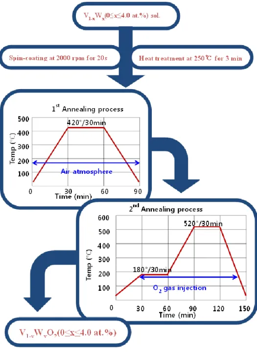
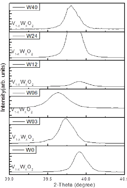
본 연구에서는 W 이온이 첨가된 V1-xWxO2(0≤x≤4.0 at.%)박막을 솔-겔 법으로 제 조하였다. W 이온의 첨가농도는 0~4.0 at.%로 두었고, 박막 제조 후 박막의 결정성 및 조성 등을 조사하기 위하여 표면 및 단면을 FE-SEM(Scanning Electron Microscopy)을 통해 관측했으며, XRD(X-Ray Diffraction) 2θ-ω scan 측정법을 이 용하여 Out-of-plane 격자 구조를 측정했다. 또한 V1-xWxO2(0≤x≤4.0 at.%)박막의 전기적 특성을 조사하기 위해 4-프로브 법을 이용하여 온도-저항 의존도를 측정하 였으며 완성된 박막으로 2 단자 소자를 제작하여 전류-전압 곡선을 반도체 파라미 터 분석기를 이용하여 측정하였다. 아래의 그림 2-16은 솔-겔 법으로 V1-xWxO2(0≤x≤4.0 at.%)박막을 제조하기 위한 흐름도이다. W 이온이 첨가된 최종 용액을 스핀-코팅하여 2 인치 사파이어기판 위에 균일한 박막을 증착하게 된다. 이 때 박막의 균일성을 확보하기 위하여 기판의 회 전 수와 Hot plate 의 Baking 온도가 중요하다. 박막의 두께는 스핀-코팅된 횟수로 조절이 가능하다. 1 회당 ≈ 30nm 두께의 막이 형성하는 것을 측정한 후 총 3 회 스핀 -코팅을 반복하여 ≈ 100nm 두께의 박막을 형성시켰다.스핀-코팅한 박막은 비정질 상태로 유기물만 휘발된 상태이다. 먼저 대기압 상태 에서 전기로를 이용하여 V2O5상을 형성한 후 산소분위기에서 저압 열처리를 진행하 여 최종적으로 VO2 상을 얻었다. VO2 상을 형성하기 위한 저압 열처리는 진공도 30mTorr 와 기판 온도 520℃에서 30 분간 진행했다. VO2상을 얻은 후 온도변화에 따 른 VO2 막질의 변형을 최소화하기 위하여 열처리 과정이 끝날 때까지 산소분압과 진공도를 지속적으로 유지시켜주는 것이 중요하다. V1-xWxO2(0≤x≤4.0 at.%)박막의 결정성을 조사하기 위하여, XRD(X-Ray
Diffraction) 2θ-ω scan 측정법을 이용하여 Out-of-plane 격자 구조를 측정했다. 그림 2-17에서 보면 Al2O3 피크인 (205)피크와 VO2 피크인 (002) 피크만 나타나 VO2
가 Al2O3기판 위에 한 방향으로 우선 배향되었음을 알 수 있다. 또한 그림 2-18에
서와 같이 텅스텐 불순물이 VO2의 결정성에 영향을 미치는 것을 관측할 수 있고,
특히 이는 VO2 피크의 이동으로 텅스텐 불순물이 VO2의 격자상수를 변화시키는 것
그림 2-16. 솔-겔 법을 이용하여 V1-xWxO2(0≤x≤4.0 at.%)박막을 제조하기 위한 흐
그림 2-18. V1-xWxO2(0≤x≤4.0 at.%)박막의 XRD 패턴에서 VO2피크를 확대한 그림.
텅스텐 불순물이 첨가됨에 따라 VO2의 격자상수를 변화시켜, VO2 피크의 체계적인
피크 이동을 예상하였으나, VO2피크를 확대하여 관측한 결과 텅스텐 함량 1.2at.%
V1-xWxO2(0≤x≤4.0 at.%)박막의 표면을 그림 2-19와 같이 SEM 이미지를 통해 관측 할 수 있고, 그림 4 에서와 같이 VO2 의 표면이 그레인 형태로 잘 형성되어있으며 그레인 경계를 육안으로 관측할 수 있다. 또한 그림 2-20에서 보이는 바와 같이 V1-xWxO2(0≤x≤4.0 at.%)박막은 모두 ≈ 100nm 즉, 같은 두께에서 실험이 진행되었다 는 것을 확인할 수 있다. 그림 2-19. V1-xWxO2(0≤x≤4.0 at.%)박막 표면의 SEM 이미지
그림 2-20. V1-xWxO2(0≤x≤4.0 at.%)박막 단면의 SEM 이미지 텅스텐 불순물이 첨가된 박막의 온도-저항 의존도를 측정해보면 각 불순물 함량 에 따른 박막의 전이특성 변화폭을 관측할 수 있다. 그림 2-21에서는 V1-xWxO2(0≤x≤4.0 at.%)박막의 온도-저항 의존도를 보이고 있으며 이 그래프를 통 해 텅스텐 불순물 즉, W 이온이 증가 할수록 VO2의 전이온도가 점점 당겨지는 것을 알 수 있다. 그림 2-22에서는 텅스텐 불순물 함량에 따른 체계적인 임계온도 변화
를 관측할 수 있다.
그림 2-21. V1-xWxO2(0≤x≤4.0 at.%)박막의 히스테리시스 곡선.
그림 2-23. 텅스텐 불순물 첨가량에 따른 전이온도 변화.
위와 같이 성장 된 텅스텐 불순물이 첨가된 박막을 이용하여 2 단자 소자를 제조했 고, 이 2 단자 소자의 전기적 특성을 파악하기 위해 파라미터 애널라이저를 사용하 여 전류-전압 특성 곡선을 그렸다. 그림 2-25. V1-xWxO2(0≤x≤4.0 at.%)박막을 이용하여 제작한 2단자 소자와 소자 제 작용 마스크의 도면 그림 2-25와 같이 제조된 2 단자 소자를 체계적으로 측정하기 위해서 VO2 채널의 폭과 길이를 각 3μm, 5μm, 10μm, 20μm, 30μm, 50μm, 100μm 단위로 변화를 주 어 제작하였으나 플라즈마 에칭 공정상의 문제로 3μm 와 5μm 단위의 채널은 제작 할 수 없었고 이렇게 측정 된 NDR 피크 또한 다양한 텅스텐 불순물 첨가량에 따라 측정되어야 한다. 그림 2-26과 그림 2-27그래프는 텅스텐 불순물이 0.3at.%인 VO2 의 전류-전압 특 성곡선을 그린 그래프들이며 이 그래프에서 NDR 현상을 목격할 수 있다. 앞으로 텅 스텐 첨가량이 다양한 VO2에서 전류-전압 특성을 측정 할 계획이다.