First-principles study on secondary electron emission of MgO surface
Youngmi Cho and Changwook KimHyo-Shin AhnEunae Cho, Tae-Eun Kim, and Seungwu Han
Citation: Journal of Applied Physics 101, 083710 (2007); doi: 10.1063/1.2721857 View online: http://dx.doi.org/10.1063/1.2721857
View Table of Contents: http://aip.scitation.org/toc/jap/101/8
First-principles study on secondary electron emission of MgO surface
Youngmi Cho and Changwook KimCAE Team, Samsung SDI, Co., Ltd., Yongin 446-557, Korea Hyo-Shin Ahn
Center for Strongly Correlated Materials Research, Seoul National University, Seoul 151-747, Korea Eunae Cho, Tae-Eun Kim, and Seungwu Hana兲
Department of Physics, Ewha Womans University, Seoul 120-750, Korea
共Received 24 January 2007; accepted 27 February 2007; published online 30 April 2007兲
We theoretically investigate secondary-electron-emission properties of MgO when noble gases are incident on the surface. We consider both potential and kinetic emission mechanisms. For the potential emission through Auger neutralization, densities of states and vacuum level are obtained from the first-principles calculations. It is found that secondary-emission coefficients decrease in the following sequence of surface directions;共111兲-OH⬎共100兲⬎共110兲, a tendency that is in agreement with experimental observations. For a surface model including F center, the secondary-emission coefficient substantially increases for Kr and Xe. To investigate the kinetic emission mechanism by an energetic ion impinging on MgO surfaces, first-principles molecular dynamics simulations are performed. Dynamic up-shifts of antibonding states between ions and oxygen atoms are found to lead to the secondary-electron emission at kinetic energies as low as 30 eV. Various collision conditions are compared based on the temporal interval during which excited states stay within the conduction band. © 2007 American Institute of Physics.关DOI:10.1063/1.2721857兴
I. INTRODUCTION
As the size of discharge cells in a plasma display cell 共PDP兲 is reduced toward the production of high-definition television, the luminescence of each cell has become a main issue.1 To improve the luminescence efficiency, cell struc-tures, gas compositions, and driving waveforms have been optimized. Recently, it has been realized that the lumines-cence efficiency, as well as the overall lifetime or stability of the device, are significantly influenced by the protective layer.2There are several material properties required for an ideal protective layer: large secondary-electron-emission 共SEE兲 coefficients, low sputtering rates, and good transpar-ency. Among the materials satisfying these conditions,3,4 MgO was most widely used until now. Owing to the high SEE coefficients, MgO layers play an important role in low-ering the firing voltage, which is directly related to the power consumption of the cell.5
In spite of its paramount importance, the relationship between material properties of thin MgO layer and discharge performance are barely revealed.6,7For example, many stud-ies reported dependence of SEE coefficients of MgO on the growth direction but the microscopic origin is yet to be understood.5,8 Such a lack of information is now posing a barrier to optimize the discharge cell through materials engi-neering. To understand the complicated surface-ion interac-tion between the discharge gas and MgO surface, theoretical analysis is required in parallel with extensive experimental measurements. In fact, the surface charging on insulators prohibits precise measurements of SEE coefficients. The
quantum-mechanical nature of SEE processes indicates that first-principles modeling could be a very useful tool for un-derstanding SEE phenomena. However, there are few theo-retical attempts to study material properties of MgO in view of its functions in PDP discharge cell.9 Motivated by these situations, we employ in this work first-principles ap-proaches to study SEE phenomena of MgO.
The emission mechanism of secondary electrons from MgO surface can be divided according to the source of stimulation, origin of emitted electrons, and physical/ chemical processes of the emission.10 In the present work, we mainly discuss the SEE mechanisms associated with surface-ion interactions, which have been known as domi-nant mechanisms in the cell of PDP during operation. We specifically focus on two processes leading to SEE; potential and kinetic emissions. In the case of the potential emission mechanism,3,11electrons are emitted through the Auger pro-cess and the energy transfer occurs via neutralization of ions. On the other hand, the transfer of kinetic energy of incoming ions to the electrons bound at surface leads to the emission in the kinetic mechanism.12This paper is organized as follows: in Sec. II, we will discuss the potential and kinetic emission mechanisms in more detail. The computational setup will be presented in Sec. III. Computational results and discussions are given in Sec. IV. Section V summarizes main results.
II. THEORETICAL BACKGROUND A. Potential emission mechanism
The potential emission is the major source of the second-ary electron emission by the ionized particles. In this mecha-nism, electrons are emitted to the vacuum through the Auger process, which is stimulated by the energy conversion that a兲Author to whom correspondence should be addressed; electronic mail:
occurs when the incoming ions are neutralized by electrons bound at the MgO surface.3,11 There are two experimental observations that are consistent with the potential emission: 共i兲 The SEE coefficient increases with the ionization energy of the incoming ion. 共ii兲 The kinetic energy of the emitted electrons depends on the electronic properties of the surface such as energy gaps and electron affinities. These character-istics are represented by Eq.共1兲:3
EK
max
= Ei− 2共Eg+兲, 共1兲
where EK
max
is the maximum kinetic energy of the secondary electron, Eiis the ionization energy of the incoming ion, and
Egandare band gap and the electron affinity of the surface,
respectively.
Theoretically, the quantitative analysis of the Auger pro-cess is feasible if one assumes a constant probability for every electronic transition involved in the electron emission. The resulting formula to calculate SEE coefficient共␥N兲 is as follows:13 ␥N =
冕
max兵Ei−0,0其 Ei−2+0 Pe共兲Dc共兲T ⫻冋
+ 0− Ei 2册
d冒
冕
max兵E i−0,c其 Ei−2+0 Dc共兲T ⫻冋
+ 0− Ei 2册
d, 共2兲where0 andcare the vacuum level and conduction
mini-mum measured from the valence bottom,is the work func-tion, and Dc共兲 is the density of states for conduction bands.
Pe and T are functions to describe escape probability and
Auger transformation of the density of states, respectively.
Peis given as follows: Pe共兲 = 1 2
冋
1 −冉
0 冊
册
␣ , 共3兲where␣ and are adjustable parameters. We use ␣= 0.248 and= 1.0 from Ref.11. On the other hand, the Auger trans-form is given below:
T
冋
+ 0− Ei 2册
=冕
0 v冕
0 v Dv共1兲Dv共2兲 ⫻␦共 − 1−2+0− Ei兲d1d2, 共4兲wherevand Dv共兲 are the valence top and density of states
for conduction bands, respectively. The delta function in Eq.
共4兲 allows for electronic transitions that satisfy the energy conservation. So far, theoretical modeling to calculate ␥N
usually assumed simplified, bulklike band structures.11,13,14 However, the Auger neutralization is a surface-specific pro-cess and therefore sensitive to surface conditions. In order to describe the surface properties realistically, we obtain0,, Dv共兲, and Dc共兲 from the first-principles calculation. This
approach allows for investigating effects of various surface conditions on SEE coefficients. In evaluating ␥N, the band gap is an essential parameter. However, it is well known that the local density approximation underestimates the energy gap by 30% − 40%. In order to overcome this limitation, we
refer to GW results in Ref.15and correct the energy gap by shifting valence and conduction bands rigidly by −2.4 eV and +0.5 eV, respectively.
B. Kinetic emission mechanism
In the kinetic emission, the conversion of kinetic ener-gies of incoming ions to the electronic transition is respon-sible for the electron emission. Experimentally, this mecha-nism is evidenced in the following observations: The SEE coefficient increases as the incident energy of ion increases.8,12,16Within the potential emission mechanism, the velocity of the ion could shift neutralization points above the surface. The interaction with image charges within dielec-trics then changes the energy transfer by up to 1 eV. How-ever, this is not enough to explain a large variation of SEE coefficients found in the literature. In addition, the energy distributions of emitted electrons are similar for various ion types, which is not explained by potential emission mechanism.12 Therefore, it is likely that the kinetic energy plays a direct role in increasing the SEE coefficient. In the case of metallic surfaces, the kinetic emission is observed with ions with large kinetic energies typically of the order of keV. By contrast, insulating surfaces begin to show signa-tures of kinetic emission at much lower energies below 100 eV.8,12,16 This implies that the emission mechanism of the insulating surface due to slow ions is fundamentally different from the case for metallic surfaces. In Ref. 12, it was sug-gested that the electronic excitation into the surface exciton can account for the kinetic emission. However, a micro-scopic explanation is still in demand.
III. COMPUTATIONAL SETUP
The electronic structures of various MgO surfaces at the optimized geometries are calculated with first-principles den-sity functional calculations using a plane-wave basis set. We use the Vienna Ab-initio Simulation Package 共VASP兲 throughout this work.17The ionic potentials are described by projector-augmented-wave method18 and the exchange-correlation energy of the electrons is described within a gen-eralized gradient approximation.19The energy cutoff of 400 eV is used to generate a plane wave basis set. For the k-point integration, we use a 4⫻4⫻4 mesh for the cubic unit cell of bulk MgO and equivalent densities of mesh points for vari-ous surface models. The atomic coordinates are relaxed until the Hellmann-Feynman forces for each atom are reduced to within 0.02 eV/ Å. The vacuum length is set to 10 Å. The lattice constant of bulk MgO is computed to be 4.238 Å in comparison with experimental value of 4.211 Å. The number of layers共6−8兲 in the surface model is chosen so as to re-cover the bulk property in the middle layer. To obtain the vacuum level from the first-principles calculation, the poten-tials are averaged over the plane normal to surfaces and the vacuum level is set to the potential value in the middle of the vacuum.
We try to address the kinetic emission by performing first-principles molecular dynamics simulation 共FPMD兲 for the collision between the ion and MgO surface. The compu-tational framework and parameters are similar to those used
in the static electronic-structure calculation as detailed in the above. Since the ions are mostly neutralized just before col-lision events 共⬃3 Å above the surface兲, we calculate with neutral atoms incident on the surface. The molecular dynam-ics is carried out within the microcanonical ensemble, i.e., along the constant-energy trajectory. The time step is set to 1 fs and the total energy is conserved within 3 meV/atom dur-ing the total simulation time of 200 fs. The共100兲 slab models with six layers are used with 2
冑
2⫻2冑
2 periodicity along the lateral directions. The bottom layer of the slab is fixed to prevent the drift of model systems.IV. RESULTS AND DISCUSSION
A. Potential emission properties of various types of surfaces
We first examine the dependence of SEE coefficients 共␥N兲 on the surface direction by performing calculations on
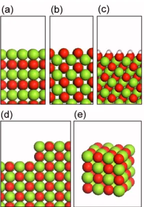
the共100兲, 共110兲, and 共111兲 surfaces, the main low-index sur-faces of rocksalt structures.关See Figs. 1共a兲–1共c兲.兴 These are also growth directions frequently observed for MgO protec-tive layer. The bulk-terminated 共111兲 surface is polar and electrically unstable. We passivate the oxygen-terminated 共111兲 surface by attaching a hydrogen atom on top of each oxygen atom. The hydrogenated共111兲-共1⫻1兲 surface关共111兲-OH, hereafter兴 was reported to be more stable than the 共100兲 surface.20 The computed band structure of each surface is shown in Figs.2共a兲–2共c兲. Compared to the bulk, new states develop below the conduction bands. The inspection of the squared wave function indicates that these states are distrib-uted outside the MgO surface and extend as much as 6 Å.
This state lies just below the vacuum level and is usually known as an image state. The presence of image states for a MgO surface was also reported in the GW calculation,15 al-though the energy level in our results is slightly downshifted compared to the GW estimation. Since these states are bound at the surface, it has small but adverse effects on the SEE coefficients by increasing the denominator in Eq. 共2兲. The work functions, which are set to the relative position of the valence top from the vacuum, are shown in TableIfor共100兲,
FIG. 1.共Color online兲 Atomic geometry of various model systems. 共a兲 共100兲 surface,共b兲 共110兲 surface, 共c兲 共111兲-OH surface, 共d兲 surface step, and 共e兲 nanocube. The light and dark spheres indicate Mg and O atoms, respec-tively. The hydrogen atoms in共c兲 are denoted by small spheres.
FIG. 2. Band structures of various surface models. 共a兲 共100兲 surface. 共b兲 共110兲 surface. 共c兲 共111兲-OH surface. 共d兲 Surface step. For each band struc-ture, top views of surface unit cells are also shown on top of each figure. The Fermi level is set to zero共horizontal dashed lines兲.
TABLE I. Computed SEE coefficients for Auger neutralization process. The work functions are given by the energy difference between the highest oc-cupied state and the vacuum. The band gap is corrected by the scissor operation. The ionization energies in eV are given in the parentheses of each noble gas.
共100兲 共110兲 共111兲 Step Cube F
center
V
center Work function共eV兲 7.485 6.886 5.715 7.560 6.797 5.349 7.869 He共24.58兲 0.379 0.371 0.412 0.377 0.385 0.368 0.373 Ne共21.56兲 0.340 0.323 0.393 0.334 0.343 0.317 0.328 Ar共15.76兲 0.174 0.096 0.328 0.163 0.199 0.110 0.129 Kr共14.00兲 0.0 0.0 0.166 0.0 0.004 0.043 0.0 Xe共12.13兲 0.0 0.0 0.008 0.0 0.0 0.257 0.0
共110兲, and 共111兲-OH surfaces. The charge transfer between oxygen and hydrogen atoms forms effective dipole layers between 共111兲-OH and the vacuum and reduces the work function of the共111兲-OH surface substantially.
The SEE coefficients共␥N兲 are calculated by evaluating
Eq. 共2兲 with density of states and work functions obtained from first-principles calculations. As mentioned in the above, the underestimate of the energy gap is corrected with refer-ence to GW data for共100兲 surface. We assume that the scis-sor operation can be uniformly applied irrespective of the surface direction and shift valence and conduction bands with equal amounts to those for the 共100兲 direction. The computational results for ␥N for the representative surfaces
with various noble gases are compiled in TableI. First, it is found that ␥N increases monotonically with the ionization energy. The larger ionization energy facilitates transitions into higher energy above the vacuum and results in enhanced SEE coefficients. This is in accordance with the experimental reports and other theoretical estimates.13 Regarding the ori-entation of surfaces, SEE coefficients are found to increase in the following order: 共110兲⬍共100兲⬍共111兲-OH. The largest
␥N
for共111兲-OH can be explained on the basis of the reduced work function. On the other hand, the larger density of image states for the共110兲 surface below the vacuum level explains the smallest SEE coefficients. The dependence of␥Non the surface direction agrees well with experimental results.5,8 However, it should be noted that surfaces in experiments are frequently terminated with 共100兲 micro-facets and precise comparison should be accompanied with the analysis on the surface morphology.
Next, we examine the effect of topological defects on SEE coefficients. Compared to bulk MgO, new absorption peaks have been observed for MgO surfaces by high-resolution electron energy loss spectroscopy and the diffuse reflectance spectroscopy.21,22The ab initio Hartree-Folk cal-culations showed that these peaks originated from the topo-logical defects of surfaces such as steps, kinks, and corners.23 In Fig.1共d兲, a model geometry imitating a MgO共100兲 sur-face including a step structure is shown and the computed band structure is given in Fig. 2共d兲. The flat bands are no-ticeable in conduction bands due to the localized states that originated from the step edge. Steps with different depths are also computed but the band structures are very similar to that of the double steps in Fig. 2共d兲. The calculated␥N for the
step model is shown in TableI. Since the work function and electronic structure are close to those of the clean共100兲 sur-face,␥N is almost identical to the values for the 共100兲
sur-face. In addition to the step, various types of corners are also important topological defects on the MgO surface. Including corner defects increases the size of the supercell signifi-cantly. Instead, we calculate on a nano-sized MgO cluster with 64 atoms 共32 anions and 32 cations兲, which includes corners as well as edges.关See Fig. 1共e兲.兴 We find that states localized at the corner site appear⬃2 eV above the valence top. However, its impact on the SEE coefficient is negligible as shown in TableI.
B. Potential emission properties of surfaces with vacancies
The presence of point defects in MgO has been known to result in a variety of optical, catalytic, and electrical phenomena.24The structural and electronic characterizations of these defects are detrimental to understanding material properties of MgO. So far, little is known about the correla-tion between the vacancy defects and SEE from MgO sur-faces. The point defects such as F centers共oxygen vacancies兲 and V centers共magnesium vacancies兲 can be included within the material during the deposition process or generated dur-ing the agdur-ing process used in activatdur-ing the discharge cell. In fact, recent experimental results show that the existence of F centers in MgO decreases firing voltage.25 A theoretical model was introduced to explain these results, assuming sim-plified electronic structures.14 Based on the first-principles approaches, we study the effects of representative point va-cancy defects on the electronic properties and SEE charac-teristics of MgO.
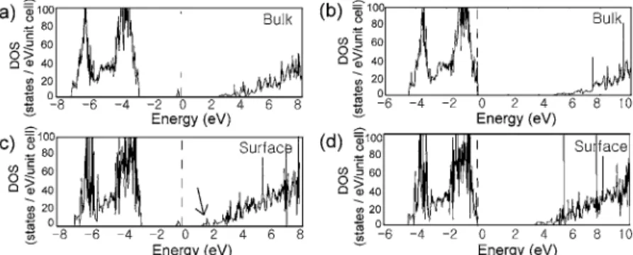
The vacancies are created on 共100兲 surfaces with the lateral periodicity of 3⫻3. The atoms are removed sym-metrically from both sides of the slab to keep the averaged potential flat in the vacuum region. The computed DOS are shown in Fig. 3. For comparison, the DOS for the bulk model including vacancies are also displayed. The F center energies are 2.4 and 2.2 eV from the valence top for the bulk and the surface, respectively. These values are in good agree-ment with previous computational results.26In the case of V center, no defect levels are identified within the energy gap. Instead, the Mg vacancy induces delocalized hole states near the valence top. For F centers, localized bands are found just below the conduction bottom 关see an arrow in Fig. 3共c兲兴. These states originated from the image states and can be conceived as perturbed states due to changes in electrostatic potentials near the defect sites.
FIG. 3. Density of states共DOS兲 for F and V centers in the bulk or on the共100兲 surface. 共a兲 and 共c兲 are DOS’s for F center and共b兲 and 共d兲 are those for V center. The Fermi level is set to zero共vertical dashed lines兲. An arrow in共c兲 indicates localized surface states developed below the conduction band.
The computed␥N values for the surface with point de-fects are listed in TableI. We find that the V center has little influence on the SEE characteristics, which is reasonable be-cause the work function and DOS are very similar to those for the clean surface. The slight decreases are attributed to the larger work function. On the other hand, the F center substantially affects SEE for ions with small ionization ener-gies, such as Kr and Xe atoms. Note that these ions do not contribute to SEE by Auger neutralization process for perfect 共100兲 surfaces. The mid-gap states associated with the F cen-ter enable the electrons to excite above the vacuum level. These results are good in comparison with previous results.14,25
C. Kinetic emission—basic principle
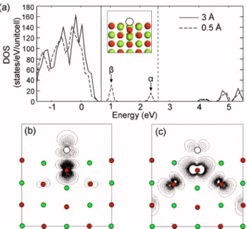
Before carrying out full-scale FPMD simulations, we ex-amine how the electronic structure is affected as an atom approaches to the MgO surface. For this, we perform static calculations with various distances between an ion 共an Ar atom in this case兲 and the surface. The positions of Ar atoms and ions in the bottom layer of the MgO slab are fixed while all other atoms are relaxed. The inset in Fig. 4共a兲 shows relaxed geometries when the Ar atom is above the surface by 0.5 Å. Laterally, the Ar atom is on top of the oxygen atom in the top layer. The relaxed distance between O and Ar atoms is 1.3 Å. The DOS in Fig. 4共a兲 shows the electronic struc-tures for two different ion-surface separations. When the Ar atom is close to the surface, new states 共indicated as␣ and
兲 are created within the band gap. The contour plots of these states are shown in Figs.4共b兲and4共c兲. It can be found that the ␣ state originated from the antibonding between Ar-p and O-p orbitals. On the other hand, the  state is composed of mainly p orbitals of oxygen atoms in the first
and second layers that are close in distance. The antibonding character can be also confirmed from the nodal structures in between atomic orbitals. With the new localized state fully occupied, the Fermi level rises into the energy gap of MgO. Further approach of the ion to the surface causes the local-ized state to climb over the conduction bottom and eventu-ally reach the vacuum level. This will lead to a finite prob-ability of those states jumping into the vacuum, hence the secondary electron emission.共Note that the emission process is beyond the adiabatic approximation employed in this work and the rise of the Fermi level stops near the conduction bottom.兲 The emission into the vacuum state is facilitated by the negative electron affinity of the MgO共100兲 surface. On the other hand, when the Ar atom is pushed on top of the Mg atom, we do not identify any state developed within the en-ergy gap.
Next, we carry out FPMD simulation on the Ar atom colliding vertically with the oxygen atom in the MgO surface with kinetic energies of 10 or 30 eV. In Fig.5, the distance between Ar and O atoms, and the position of the Fermi level are plotted as a function of time. With higher kinetic ener-gies, the Ar atom penetrates deeper into the surface. In addi-tion, the Fermi level shifts up toward the conduction band as found in the above static simulations. The electron emission could occur when the defect levels are above the vacuum level. It is noticeable that the Fermi level briefly touches the conduction bottom at a kinetic energy of 30 eV 关see Fig.
5共b兲兴. Since the conduction bottom is close to the vacuum level, the threshold energy for kinetic emission would be close to this value. It is beyond the scope of this work to obtain SEE coefficients directly from FPMD simulations. In-stead, we define the “ ‘excitation’ time” 共ex兲 as a working parameter by integrating total time during which the Fermi level is above the conduction bottom. We assume that ex correlates well with the escape probability of the electron and compareexfor various conditions in the next section.
D. Kinetic emission properties—parameter dependence
In order to study how the kinetic electron emission de-pends on the ion species and incident directions, we perform FPMD simulations with various conditions of incoming noble gases, such as atomic species, impact points on MgO, incident energies, and collision angles. We choose Ne and Xe
FIG. 4. 共Color online兲 共a兲 Density of states when the Ar atom is above the surface by 3 or 0.5 Å. The Fermi level is indicated by vertical lines. The localized states共␣and兲 are indicated by vertical arrows. The inset shows the relaxed geometry when the Ar-surface distance is 0.5 Å. Note that the O atom below the Ar atom is relaxed downward substantially.共b兲, 共c兲: Contour plots of␣andstates in共a兲, respectively. Light and dark grays indicate Mg and O atoms, respectively. The Ar atom is denoted by empty circles.
FIG. 5. Changes of the Fermi level and distances between Ar and O atoms 共dAr-O兲 during the molecular dynamics simulations when Ar atoms impinge
on the共100兲 surface with initial kinetic energies of 共a兲 10 eV and 共b兲 30 eV. The conduction bottom is indicated by horizontal dashed lines.
atoms for the detailed investigation because they constitute primary plasma gases in PDP cells. The impact points are selected on 4⫻4 uniform grids on
冑
2⫻冑
2 unit cell of共100兲 surface, and the incoming direction is set to具001典 or 具111典. This is to simulate ions colliding on surfaces with the growth direction of 共100兲 and 共111兲, respectively; in the discharge cell, most ions arrive at the MgO surface from the normal direction. Since the共111兲-textured surface is usually faceted with共100兲 surfaces in a triangular pyramid, the normal inci-dences on those surfaces are equivalent to a collision on a 共100兲 surface with the angle of − arctan共冑
2兲 共in radians兲 from the surface normal vector. We choose具111典 as a repre-sentative direction. The distributions of kinetic energies of ions were estimated by Monte Carlo simulations,27,28 and they exhibit exponential decays with respect to the kinetic energy. Considering that the SEE coefficient scales almost linearly with the kinetic energy, ions with kinetic energies of 30− 60 eV will play a dominant role in the kinetic emission. We perform FPMD simulations for the time interval of 200 fs, which turn out to be enough to measureexup to the kinetic energy of 100 eV. The ex’s averaged over impact points are compiled in Table II. Several key features merit discussions:共i兲 It is noticeable that Xe, which does not con-tribute to SEE by Auger neutralization, is able to produce secondary electrons through the kinetic emission mechanism. This is an interesting observation because a PDP cell typi-cally operates with Ne-Xe gas mixtures. In addition, the sur-face of MgO is exposed to continuous collisions with Xe atoms with the mean kinetic energy bigger than that of Ne atoms.27,28 共ii兲 Even though Ne atoms would efficiently transfer energies to oxygen atoms owing to the similar atomic mass, exis higher for Xe atoms. This is due to the much larger ionic mass of Xe atoms, which allows for longer collision times.共iii兲 For Ne atom, the 具111典 direction is more efficient than the具001典 direction to extendex. The impacts along the 具111典 direction efficiently induce subsequent col-lisions between oxygen atoms. This promotes the electronic excitation through the antibonding between oxygen p orbit-als 共see the previous section兲 and therefore leads to pro-longedex. On the other hand, the collision with Xe atoms is less sensitive to the direction, which is understandable con-sidering the larger atomic radius of Xe atoms共1.24 Å兲 com-pared to that of Ne atoms共0.51 Å兲.V. SUMMARY
In summary, we have introduced first-principles methods to investigate secondary electron emission properties of MgO surface used as a protective layer in PDP. The surface-dependent electronic structures and work functions were
ob-tained from the density functional calculations. The SEE co-efficients depending on the surface direction are in good comparison with experimental observations. The 共111兲-OH surface was found to enhance SEE coefficients for all noble gases owing to the surface dipole lowering the work func-tion. The presence of point defects such as F centers on the surface enabled the SEE by Kr and Xe atoms. The kinetic emission mechanism, on the other hand, was addressed using the molecular dynamics simulation within the adiabatic ap-proximation. Although the emission process itself was not described by the present computational approaches, the ex-citations of energy levels were identified, which would ac-count for the main procedure leading to kinetic electron emission by slow ions. The most interesting observation would be a possible contribution of Xe atoms to the electron emission through the collision effects. This will be useful information for designing gas mixtures used in PDP.
ACKNOWLEDGMENTS
This work was supported by Samsung SDI and the Ko-rea Science and Engineering Foundation through the Basic Research program 共Grant No. R01-2006-000-10883-0兲. EC and TK appreciate financial supports by second BK21 project. The computations were carried out at Korea Institute of Science and Technology Information 共KISTI兲 through Seventh Strategic Supercomputing Program.
1M. Yoo, E. Hwang, H. Shin, D. Lee, and Y. Cho, SID Digest共Tech. Dig.
Society for Information Display, 2005兲, p. 1836.
2J. P. Boeuf, J. Phys. D 36, R53共2003兲, and references therein.
3T. J. Vink, A. R. Balkenende, R. G. F. A. Verbeek, H. A. M. van Hal, and
S. T. de Zwart, Appl. Phys. Lett. 80, 2216共2002兲.
4H. Uchiike, K. Miura, N. Nakayama, T. Shinoda, and Y. Fukushima, IEEE
Trans. Electron Devices 23, 1211共1976兲.
5V. van Elsbergen, P. K. Bachmann, and G. Zhong, Proceedings of the 7th
International Display Workshops, IDW ’00, Sendai, Japan共2000兲, p. 687.
6S. Y. Park, M. J. Lee, H. J. Kim, S. H. Moon, S. G. Kim, and J. K. Kim,
J. Vac. Sci. Technol. A 23, 1162共2005兲.
7Y. H. Cheng, H. Kupfer, and F. Richter, J. Appl. Phys. 94, 3624共2003兲. 8E. H. Choi, J. Y. Lim, Y. G. Kim, J. J. Ko, D. I. Kim, C. W. Lee, and G.
S. Cho, J. Appl. Phys. 86, 6525共1999兲.
9A. Miyamoto, R. Endou, H. Kikuchi, H. Tsuboi, M. Koyama, A. Endou,
M. Kubo, C. A. Del Carpio, and H. Kajiyama, Proceedings of the 12th International Display Workshops, IDW’05, Sendai, Japan共2005兲, p. 423.
10A. von Engel, Ionized Gases共AIP, New York, 1994兲. 11H. D. Hagstrum, Phys. Rev. 122, 83共1961兲.
12P. Riccardi, M. Ishimoto, P. Barone, and R. A. Baragiola, Surf. Sci. 571,
L305共2004兲.
13Y. Motoyama, H. Matsuzaki, and H. Murakami, IEEE Trans. Electron
Devices 48, 1568共2001兲.
14Y. Motoyama and F. Sato, IEEE Trans. Plasma Sci. 34, 336共2006兲. 15M. Rohlfing, N.-P. Wang, P. Krüger, and J. Pollmann, Phys. Rev. Lett. 91,
256802共2003兲.
16S. K. Lee, J. H. Kim, J. Lee, and K.-W. Whang, Thin Solid Films 435, 69
共2003兲.
17G. Kresse and J. Hafner, Phys. Rev. B 47, 558共R兲 共1993兲; 49, 14251
共1994兲.
18P. E. Blöchl, Phys. Rev. B 50, 17953共1994兲.
19J. P. Perdew, K. Burke, and M. Ernzerhof, Phys. Rev. Lett. 77, 3865
共1996兲.
20V. K. Lazarov, R. Plass, H.-C. Poon, D. K. Saldin, M. Weinert, S. A.
Chambers, and M. Gajardziska-Josifovska, Phys. Rev. B 71, 115434 共2005兲.
TABLE II. Computed excitation time in femtoseconds with respect to ki-netic energies, directions, and species of incident ions.
Energy共eV兲 Direction Ne Xe
30 具001典 4 15.8
50 具001典 6.25 28.3
100 具001典 4.75 28.63
100 具111典 8.25 25.63
21J. S. Ferrer, J. M. Rojo, M. Salmeron, and G. A. Somorjai, Philos. Mag. A 45, 261共1982兲.
22S. Coluccia, A. Barton, and A. J. Tench, J. Chem. Soc., Faraday Trans. 1 77, 2203共1981兲.
23A. L. Shluger, P. V. Sushko, and L. N. Kantorovich, Phys. Rev. B 59, 2417
共1999兲.
24A. Gibson, R. Haydock, and J. P. LaFemina, Phys. Rev. B 50, 2582
共1994兲.
25Y. Motoyama, Y. Hirano, K. Ishii, Y. Murakami, and F. Sato, J. Appl.
Phys. 95, 8419共2004兲.
26L. N. Kantorovich, J. M. Holender, and M. J. Gillan, Surf. Sci. 343, 221
共1995兲.
27S. J. Yoon and I. Lee, J. Appl. Phys. 91, 2487共2002兲.
28L. C. Pitchford, J. Wang, D. Piscitelli, and J. P. Boeuf, IEEE Trans. Plasma