저작자표시-비영리-변경금지 2.0 대한민국 이용자는 아래의 조건을 따르는 경우에 한하여 자유롭게 l 이 저작물을 복제, 배포, 전송, 전시, 공연 및 방송할 수 있습니다. 다음과 같은 조건을 따라야 합니다: l 귀하는, 이 저작물의 재이용이나 배포의 경우, 이 저작물에 적용된 이용허락조건 을 명확하게 나타내어야 합니다. l 저작권자로부터 별도의 허가를 받으면 이러한 조건들은 적용되지 않습니다. 저작권법에 따른 이용자의 권리는 위의 내용에 의하여 영향을 받지 않습니다. 이것은 이용허락규약(Legal Code)을 이해하기 쉽게 요약한 것입니다. Disclaimer 저작자표시. 귀하는 원저작자를 표시하여야 합니다. 비영리. 귀하는 이 저작물을 영리 목적으로 이용할 수 없습니다. 변경금지. 귀하는 이 저작물을 개작, 변형 또는 가공할 수 없습니다.
A DOCTORAL DISSERTATION
Development of the DC-RF Hybrid Plasma
Source and the Application to the Etching and
Texturing of the Silicon Surface
Department of Nuclear & Energy Engineering
Graduate School
Jeju National University
Ji Hun Kim
Ph. D. DISSERTATION
Development of the DC-RF Hybrid Plasma
Source and the Application to the Etching and
Texturing of the Silicon Surface
Department of Nuclear & Energy Engineering
Graduate School
Jeju National University
Ji Hun Kim
博 士 學 位 論 文
직류 고주파 복합 플라즈마 소스
-개발 및 이를 응용한 실리콘 표면
식각 및
Texturing
연구
濟州大學校 大學院
工 學 科
金
志
勳
2011
年
02
月
직류 고주파 복합 플라즈마 소스
-개발 및 이를 응용한 실리콘 표면
식각 및
Texturing
연구
指導敎授 李 憲 周
金 志 勳
이
論文
을
工學博士學位論文
으로
提出
함
2010
年
12
月
의
을
함
金志勳
工學 博士學位 論文
認准
審査委員長
최 치 규
( )
인
委
員
노 승 정
( )
인
委
員
유 석 재
( )
인
委
員
이 윤 준
( )
인
委
員
이 헌 주
( )
인
濟州大學校 大學院
2010
年
12
月
Development of the DC-RF Hybrid Plasma Source
and the Application to the Etching and Texturing of
the Silicon Surface
Ji-Hun Kim
(Supervised by professor Heon-Ju Lee)
A thesis submitted in partial fulfillment of the requirement for the degree of Doctor of Nuclear and Energy Engineering.
2010. 12.
This thesis has been examined and approved.
Thesis director, Heon Ju Lee, Prof. of Nuclear & Energy Engineering
Chi Kyu Choi
Seung Jeong Noh
Suk Jae Yoo
Yun Jun Lee
Heon Ju Lee
(Name and signature)
2010. 12
Date
Department of Nuclear & Energy Engineering
GRADUATE SCHOOL
C O N TEN TS
CONTENTS ··· ⅰ
LIST OF FIGURES ··· ⅴ
LIST OF TABLES ··· ⅺ
SUMMARY ··· ⅻ
. Introduction
Ⅰ
··· 1
1. Atmospheric Pressure source ··· 1
1.1 DC arc plasmatrons with hot rod cathode and cold nozzle anode ···· 2
1.2 DC arc plasmatrons with cold thermo-chemical cathode (Hf, Zr)
and cold nozzle anode ··· 2
1.3 DC arc plasmatrons with cold tubular electrodes and arc
revolving inside ··· 3
1.4 AC three-phase arc plasmatrons ··· 3
1.5 RF arc plasmatrons ··· 4
1.6 Microwave Plasmatrons ··· 4
1.7 Dielectric barrier discharge (DBD) plasma ··· 4
2. Plasma etching ··· 8
3. Plasma texturing for the solar cell ··· 9
. Theoretical Background
Ⅱ
··· 11
1. Atmospheric pressure plasma source ··· 11
1.1 DC arc plasma source ··· 11
1.2 ICP torches ··· 13
2. Plasma etching ··· 17
2.1 Etching rate, uniformity and area ··· 18
2.2 Isotropic etching and an-isotropic etching ··· 19
2.3 Parameters of the etching condition ··· 20
3. Plasma texturing for the solar cell ··· 22
3.1 Silicon texturing processing in the solar cell ··· 23
3.2 Features of the plasma texturing processing ··· 23
3.3 Advantage of the plasma texturing ··· 23
. Development of DC Arc Plasmatron
Ⅲ
··· 26
1. Development of new DC arc plasma source ··· 26
1.1 The origin of technical decision ··· 26
1.2 Main features of the plasmatron design ··· 26
1.3 Problem of the cathode ··· 31
1.4 Measurement of characteristics ··· 31
1) Evaluation of plasma temperature ··· 31
2) Measurements of the anode erosion rate ··· 32
3) Plasma temperature and density ··· 33
2. Plasmatron arc sport ··· 35
2.1 Cathode arc spot ··· 35
2.2 Main features of the plasmatron design ··· 35
3. Plasmatron characteristics ··· 36
3.1 Current/voltage ripple for inverter power source ··· 36
3.2 Experimental VACs for the DC arc discharge in the plasmatron ··· 38
1) Variation of inter-electrode distance ··· 38
3) Variation of the argon flow rate in the cathode channel ··· 40
4) Variation of gas flow rate in the Technologic channel ··· 43
3.3 Stability of arc working points for the new plasmatron ··· 45
4. Discussion ··· 45
. Development of the DC-RF Hybrid Plasma Source
Ⅳ
··· 47
1. DC-RF hybrid plasma system ··· 48
1.1 Calculation of and electric fields ··· 48
1.2 RF impedance matching ··· 52
1.3 DC-RF hybrid plasma ststem ··· 58
2. Characteristics of the DC-RF hybrid plasma ··· 60
2.1 Measurement of the discharge characteristics by IR camera ··· 61
2.2 Measurement of the plasma parameter by a Langmuir probe ··· 64
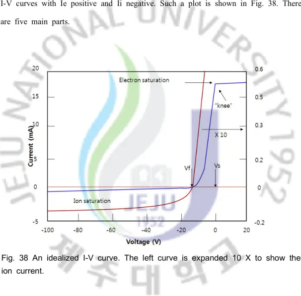
1) Parts of the I-V curve ··· 65
2) Electron temperature ··· 66
3) Electron density ··· 66
4) Experimental set-up ··· 67
5) Measurements and results ··· 68
2.3 Measurement of the optical emission spectroscopy ··· 76
2.4 Measurement of the plasma gas temperature by IR camera ··· 81
. Plasma Etching
Ⅴ
··· 84
1. Plasma etching by DC arc plasmatron at a low pressure ··· 86
1.1 Experimental set-up ··· 86
1.2 Results & discussion ··· 88
2.1 Experimental set-up ··· 97
2.2 Results & discussion ··· 99
3. Plasma etching by DC-RF hybrid system ··· 103
3.1 Experimental set-up ··· 103
3.2 Results & discussion ··· 104
. Plasma Texturing for the Solar Cell
Ⅵ
··· 105
1. Experimental set-up ··· 107
1.1 Plasma textuing at a low pressure (5 Torr) ··· 109
1.2 Plasma textuing at an atmospheric pressure ··· 109
2. Results and discussion ··· 112
2.1 Results ··· 112
2.2 Discussion ··· 121
. Conclusion
Ⅶ
··· 122
REFERENCE ··· 124
ABSTRACT (Korean) ··· 128
CURRICULUM VITA ··· 131
ACKNOWLEDGEMENT ··· 135
LIST OF FIGURE
Fig. 1 Principle of dielectric barrier discharge ··· 5
Fig. 2 Principle of arc plasma torches(left: current-carrying arc, right: transferred arc) ·
12
Fig. 3 High velocity Plazjet (Tafa, Praxair) ··· 12
Fig. 4 Sultzer Metco Triplex Ⅱ Plasma Spray Gun ··· 13
Fig. 5 RF plasma torch(Teckna Plasma system Inc). ··· 14
Fig. 6 Concept of the dielectric barrier discharge ··· 15
Fig. 7 Isotropic Etching and An-isotropic Etching ··· 19
Fig. 8 Efficiency and loss factor in solar cell ··· 22
Fig. 9 Basic concept of the silicon texturing for the solar cell ··· 25
Fig. 10 Textured Silicon Surface (wet process) ··· 25
Fig. 11 Concept of the DC arc lasmatron
(1- cathode, 2- anode,
3-technologic channel, 4- process gas supply, 5- Ar supply, 6- Ar injector,
7
–
plasma flow, 8- presumable form of plasma vortex acting as a
distributed anode spot, 9 - arc discharge column.) ··· 28
Fig. 12 Diagram of the T-plasmatron (front view) ··· 28
Fig. 13 Top view of the DC arc plasmatron ··· 29
Fig. 14
Design of A-type DC arc plasmatron··· 29
Fig. 15
Inside structure of A-type DC arc plasmatron··· 30
Fig. 16 Photo of the used copper anode ··· 33
Fig. 17 Current waveform of the DC arc plasmatron ··· 37
Fig. 18 Voltage waveform of the DC arc plasmatron ··· 37
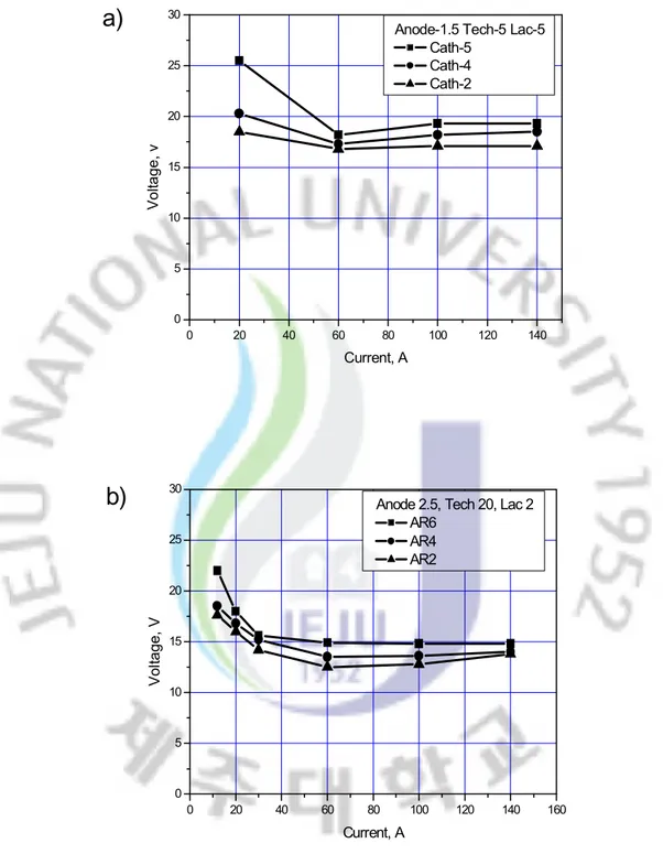
Fig. 20 VACs for anode = 1.5, 2.3 and 3.5 mm ··· 40
Fig. 21 VACs for different argon flow rates in the cathode channel ··· 42
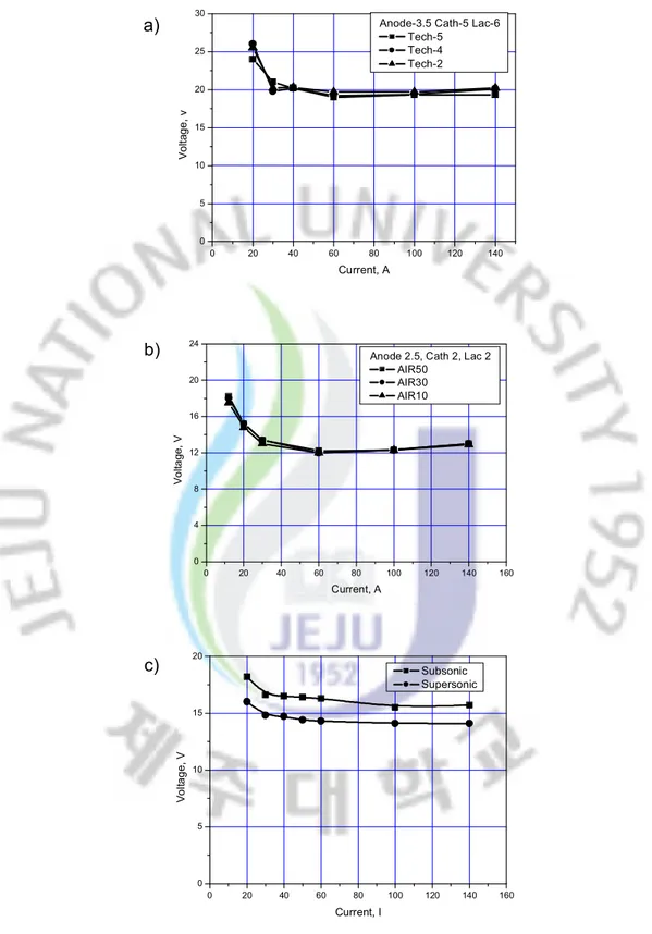
Fig. 22 VACs for different gas flow rates in the technologic channel ··· 44
Fig. 23
Calculated electric fields according to the number of turns··· 51
Fig. 24
Distribution of electric fields··· 52
Fig. 25
Source impedance driving its complex conjugate and the resulting equivalent··· 53
Fig. 26 Schematic of a DC-RF hybrid plasma and a gas injection system · 54
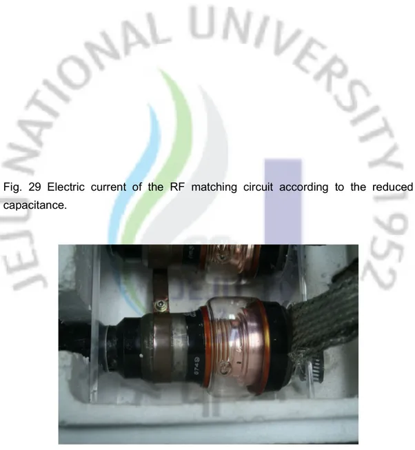
Fig. 27 Electric current of the RF matching circuit (C_T: 738.7 pF, C_R: 42.0 pF) ···
55
Fig. 28
Electric current of the RF matching circuit (C_T: 738.7 pF, C_R: 42.30 pF)55
Fig. 29 Electric current of the RF matching circuit according to the reduced
capacitance ··· 56
Fig. 30 Picture of the variable capacitor ··· 56
Fig. 31 Picture of the matching part ··· 57
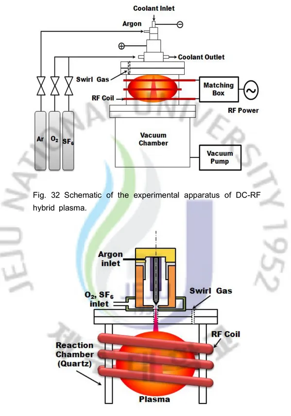
Fig. 32 Schematic of the experimental apparatus of DC-RF hybrid plasma 59
Fig. 33 Schematic of a DC-RF hybrid plasma and a gas injection system · 59
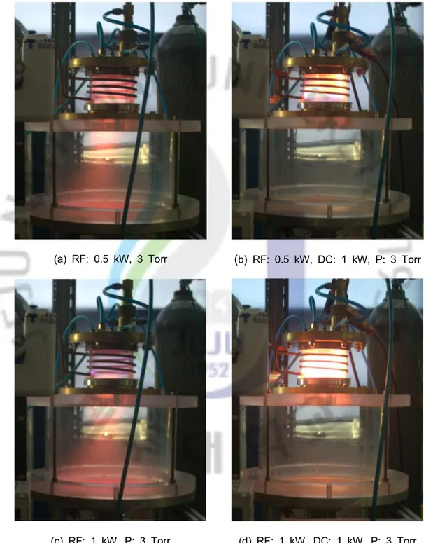
Fig. 34 Photographs of the RF and DC-RF hybrid plasma discharge ··· 61
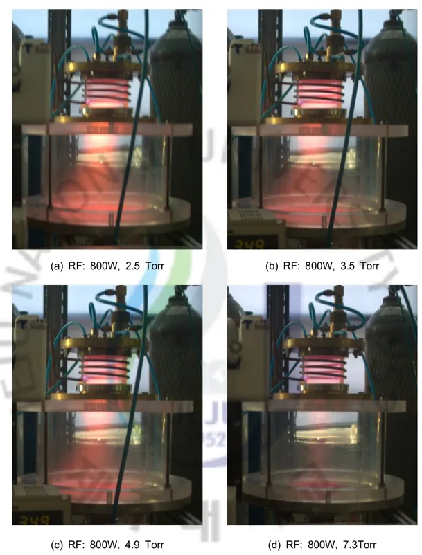
Fig. 35 Characteristics of the RF plasma discharge according to the pressure ·· 62
Fig. 36 Characteristics of the DC-RF plasma discharge according to the pressure 63
Fig. 37 Typical electrical circuit for single Langmuir probe ··· 64
Fig. 38 An idealized I-V curve. The left curve is expanded 10X to show the
ion current ··· 65
Fig. 39 DC power supply for electric probe ··· 66
Fig. 40 Installed electric probe in the reaction chamber ··· 67
Fig. 41 Measurement points of the electric probe ··· 68
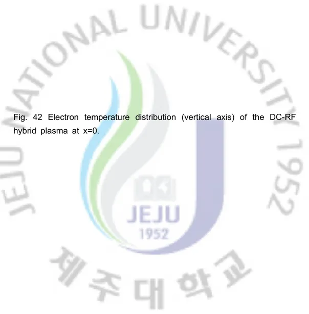
Fig. 42 Electron temperature distribution (vertical axis) of the DC-RF hybrid
plasma at x=0 ··· 69
Fig. 43 Electron temperature distribution (vertical axis) of the DC-RF hybrid
plasma at x=2 ··· 69
Fig. 44 Electron temperature distribution (vertical axis) of the DC-RF hybrid
plasma at x=4 ··· 70
Fig. 45 Electron temperature distribution (horizontal axis) of the DC-RF
hybrid plasma at y=1.5 ··· 70
Fig. 46 Electron temperature distribution (horizontal axis) of the DC-RF
hybrid plasma at y=0 ··· 71
Fig. 47 Electron temperature distribution (horizontal axis) of the DC-RF
hybrid plasma at y=-1.5 ··· 71
Fig. 48 Plasma density distribution (horizontal axis) of the DC-RF hybrid
plasma at y=0 ··· 72
Fig. 49 Plasma density distribution (horizontal axis) of the DC-RF hybrid
plasma at y=1.5 ··· 73
Fig. 50 Plasma density distribution (horizontal axis) of the DC-RF hybrid
plasma at y= -1.5 ··· 73
Fig. 51 Plasma density distribution (vertical axis) of the DC-RF hybrid
plasma at x=0 ··· 74
Fig. 52 Plasma density distribution (vertical axis) of the DC-RF hybrid
plasma at x=2 ··· 74
Fig. 53 Plasma density distribution (vertical axis) of the DC-RF hybrid
plasma at x=-2 ··· 75
Fig. 54 Argon plasma spectrum ··· 78
Fig. 55 Optical emission spectrum of argon RF plasma ··· 79
Fig. 57 IR camera measurement of DC-RF plasma (RF: 1 kW) ··· 82
Fig. 58 IR camera measurement of DC-RF plasma (RF: 1 kW, DC: 1 kW) ··· 82
Fig. 59 Plasma etching and texturing system (low pressure) ··· 87
Fig. 60 SEM images (Ar: 2,000 sccm, O
2, 300 sccm, CF
4: 50 sccm, Voltage: 15V,
Current: 100 A, P: 5 Torr) ··· 89
Fig. 61 SEM images (Ar: 2,000 sccm, O
2, 200 sccm, CF
4: 50 sccm, V: 15V,
Current: 100 A, P: 5 Torr) ··· 89
Fig. 62 SEM images (Ar: 2,000 sccm, O
2, 100 sccm, CF
4: 50 sccm, V: 15V,
Current: 100 A, P: 5 Torr) ··· 90
Fig. 63 SEM images (Ar: 2,000 sccm, O
2, 300 sccm, CF
4: 30 sccm, V: 15V,
Current: 100 A, P: 5 Torr) ··· 90
Fig. 64 SEM images (Ar: 2,000 sccm, O
2, 200 sccm, CF
4: 30 sccm, V: 15V,
Current: 100 A, P: 5 Torr) ··· 91
Fig. 65 SEM images (Ar: 2,000 sccm, O
2, 100 sccm, CF
4: 30 sccm, V: 15V,
Current: 100 A, P: 5 Torr) ··· 91
Fig. 66 SEM images (Ar: 2,000 sccm, O
2, 300 sccm, CF
4: 50 sccm, V: 15V,
Current: 50 A, P: 5 Torr) ··· 92
Fig. 67 SEM images (Ar: 2,000 sccm, O
2, 200 sccm, CF
4: 50 sccm, V: 15V,
Current: 50 A, P: 5 Torr) ··· 92
Fig. 68 SEM images (Ar: 2,000 sccm, O
2, 300 sccm, CF
4: 30 sccm, V: 15V,
Current: 50 A, P: 5 Torr) ··· 93
Fig. 69 SEM images (Ar: 2,000 sccm, O
2, 200 sccm, CF
4: 30 sccm, V: 15V,
Current: 50 A, P: 5 Torr) ··· 93
Fig. 70 Distribution of the Etching rates; (a) Ar: 2,000 sccm, O
2: 300 sccm, CF
4: 50
sccm, Current: 100 A: (b) Ar: 2,000 sccm, O
2: 100 sccm, CF
4: 50 sccm, Current:
Fig. 71 Results of the etching rates according to the oxygen flow rates ··· 95
Fig. 72 Results of the etching rates according to the CF
4flow rates ··· 95
Fig. 73 Results of the etching rates according to the DC arc plasmatron current ·· 96
Fig. 74 Plasma etching and texturing system (atmospheric pressure) ··· 98
Fig. 75 A SEM image of atmospheric pressure etching (Ar: 2,000 sccm, SF
6:
100 sccm, O
2: 200 sccm, D: 5 mm, Current: 70A) ··· 100
Fig. 76 A SEM image of atmospheric pressure etching (Ar: 2,000 sccm, SF
6:
70 sccm, O
2: 200 sccm, D: 5 mm, Current: 70A) ··· 100
Fig. 77 A SEM image of atmospheric pressure etching (Ar: 2,000 sccm, SF
6:
50 sccm, O
2: 200 sccm, D: 5 mm, Current: 70A) ··· 101
Fig. 78 A SEM image of atmospheric pressure etching (Ar: 2,000 sccm, SF
6:
100 sccm, O
2: 200 sccm, D: 10 mm, Current: 70A) ··· 101
Fig. 79 A SEM image of atmospheric pressure etching (Ar: 2,000 sccm, SF
6:
50 sccm, O
2: 200 sccm, D: 10 mm, Current: 70A) ··· 102
Fig. 80 A SEM image of atmospheric pressure etching (Ar: 2,000 sccm, SF
6:
100 sccm, O
2: 200 sccm, D: 15 mm, Current: 70A) ··· 102
Fig. 81 DC-RF hybrid plasma experimental set-up ··· 103
Fig. 82 A SEM image by the DC-RF hybrid plasma ··· 104
Fig. 83 A SEM image by the RF plasma ··· 104
Fig. 84 A schematic diagram of the A-type plasmatron: (1) cathode, (2) anode, (3)
argon supply, (4) technologic channel; (5, 6) technologic gas supply, (7)
resulting plasma flow ··· 108
Fig. 85 A diagram of the DC arc plasmatron processing system: (a) low pressure, (b)
atmospheric pressure ··· 110
Fig. 86 A picture of the DC arc plasmatron operation at low pressure (3-5mbar) 111
Fig. 87 Images of the DC arc plasmatron operating at atmospheric pressure ··· 105
Fig. 88 SEM image of the single crystalline silicon surface textured at low
pressure (3-5mbar, V=14V, D=72mm, CF4=100 sccm, Ar=2,000 sccm,
O2=500sccm, V=14V, D=72mm, CF4=100 sccm, Ar=2,000 sccm,
O2=500 sccm): (a) I=100 A, (b) I=70 A, (c) 50 A ··· 113
Fig. 89 SEM image of the single crystalline silicon surface textured with a
DC arc plasmatron current (Ar: 3000 sccm, SF
6:100 sccm, O
2:500 sccm,
Pressure: 760torr): (a) 70A, (b) 100A ··· 114
Fig. 90 SEM image of the mc-silicon surface textured at different processing
times (Ar : 3000 sccm, SF6:100sccm, O2: 500sccm, Current: 100A,
Pressure: 760torr): (a) 10 sec. (b) 30 sec. (c) 60 sec. ··· 115
Fig. 91 SEM image of the single crystalline silicon surface textured with a
oxygen concentrations (Ar : 3000 sccm, SF
6: 100 sccm, Current: 100A,
Pressue: 760torr): (a) 5%, (b) 10%, (c) 15% ··· 116
Fig. 92 SEM image of the textured amorphous silicon surface: (a) Bare
silicon, (b) textured silicon by DC arc plasmatron (Ar: 3000 sccm, SF6:
100 sccm, O2: 500 sccm, Current: 100A, Pressue: 760 torr) ··· 117
Fig. 93 SEM image of the pyramid angle to compare low and atmospheric
pressure : (a) low pressure (5 torr), (b) atmospheric pressure (760 torr) ··· 118
Fig. 94 Reflectance profile according to the plasmatron current: (t: 2min, P:
5 Torr, Ar: 3000 sccm, CF4: 90 sccm, O2: 500 sccm) ··· 119
Fig. 65 Reflectance of the textured silicon surfaces according to the DC arc
plasmatron current. (t: 30 sec., P: 760 Torr, Ar: 3000 sccm, SF6: 100
sccm, O2:500sccm) ··· 120
Fig. 96 Reflectance of the textured silicon surfaces according to the O
2concentration. (t: 30 sec., P: 760 Torr, Ar: 3000 sccm, SF
6: 100 sccm,
LIST OF TABLES
Table. 1 Characteristics of atmospheric plasma source(industrialized source) ··· 6
Table. 2 Characteristics of atmospheric plasma source(still in laboratory source) ··· 7
Table. 3 RF torches characteristics with a 6,000K Ar plasma ··· 15
Table. 4 Persistent Lines of Neutral Argon (Ar )
Ⅰ
··· 78
Table. 5 Experimental condition of the etching process at a low pressure ··· 89
Table. 6 Experimental condition of the etching process at an atmospheric
pressure ··· 100
SUMMARY
Plasma used in dry etching, thin film deposition and surface treatment for display or semiconductor industries are operating at low pressures in general. However, low pressure processing is very costly due to the use of vacuum equipment and vacuum components. Subsequent wet processing is environmentally undesirable due to the use of a large amount of chemicals. Also, the usage of vacuum processing increases fabrication cost and decreases productivity. If stable atmospheric plasmas can be used, not only the decrease in processing costs but also the increase in productivity could be obtained.
New DC arc plasmatron with a hot rod cathode and cold nozzle anode was developed and its V-A (Volt-Ampere) characteristics were investigated. Outlook of the measured V-A characteristics cleared the question of the stability of arc burning in the new DC arc plasmatron. The plasmatron that has a stable operations with distributed anode spot could possibly be applied to plasma chemical processing. And measured value of the erosion rate for copper anode is mCu » 3.6×10⁻¹⁰g/C
which is better than corresponding data for thermo-ionic emission cathodes made of tungsten mw ~10-9g/C. These facts mean that plasmatron durability reaches ~103 h.
The low anode erosion rate is related to the large surface of arc-anode contact due to distributed anode arc spot, which reduces the current density. Unique characteristics of the new plasma source concerning its durability and plasma purity at rather low temperatures make it an interesting tool for technical applications, such as etching/deposition and chemical reaction.
To apply a plasma processing, the T-type plasmatron was modified to A-type. The A-type plasmatron was used to activate the CF4 and SF6 gases in etching
the activated gas particles inside a plasmatron and let them preserve their activated state outside, the whole device was installed outside of the vacuum chamber for vacuum processing. The experiment was provided on the mono-crystalline silicon wafer. The etching was carried out with plasma consisting of SF6 (50 sccm) as a
reactive etching gas with O2 (300 sccm) as a supporting gas and Argon (2000 ~
3000 sccm) as a cathode protecting gas. Etching rates were 60 μm/min at low pressure (3-5 torr) and 300 μm/min at a atmospheric pressure. The sample was positioned in such as way that the plasma flow axis would coincide with the side facet of the silicon crystal.
A texturing process was performed on a crystalline silicon (c-Si) wafer to increase the efficiency of a solar cell by using a high durability DC arc plasma source at atmospheric pressure and low pressure. CF4 and SF6 were used as the
reactive etching gases at flow rates < 100 sccm, with O2 as the supporting gas in
the range of the 5 – 15 %. To survey the characteristics of the pyramid formation
process, plasma texturing experiments were performed by varying the working time. The optimal operating conditions of the gas flow (Ar, O2, CF4, SF6), plasmatron
current and processing time were determined. The pyramid angle was approximately 50° to 60° when a single-crystalline silicon surface was textured in a vacuum whereas it was approximately 75° to 90° when textured at atmospheric pressure. The reflectance decreases with decreasing pyramid angle. The reflectance of the bare silicon ranged from 40 % to the 60 % but that of the textured silicon was approximately 5 % to 20 %. This reflectance is quite low, approximately half that reported by other studies using wet and reactive ion etching (RIE) texturing.
Even though DC arc plasmatron has many advantages, it is difficult to apply an industry due to the small applied area. To increase an effective processing area, we suggest a DC-RF hybrid plasma system. The DC-RF hybrid plasma system was designed and made. This system consists of a DC arc plasmatron, RF parts, reaction chamber, power feeder, gas control system and vacuum system. To
emission spectroscopy), infrared (IR) light camera. For RF matching, PSIM software was used to simulate a current of an impedance coil. The results of Langmuir probe measurements, we obtain a homogeneous plasma density and electron temperature those are about 1×10¹⁰ #/cm3 and 1 - 4 eV. The DC-RF hybrid plasma source is applied for plasma etching experimental, and we obtain an etching rate of 10 m/min. through a 90 mm of reaction chamber diameter.μ
. INTRODUCTION
Ⅰ
Plasmas are chemically active media. Depending on the way they are activated and their working power, they can generate low or very high "temperature" and are referred correspondingly as cold or thermal plasmas. This wide temperature range enables various applications for plasma technologies: surface coatings, waste destruction, gas treatments, chemical synthesis, machining.
Thermal plasmas (especially arc plasma) were extensively industrialized, principally by aeronautic sectors. Cold plasma technologies have been developed in the micro-electronics but their vacuum equipment limits their implantation.
Plasma used in dry etching, thin film deposition and surface treatment for display or semiconductor industries are operating at low pressures in general. However, low pressure processing is very costly due to the use of vacuum equipment and vacuum components. Subsequent wet processing is environmentally undesirable due to the use of a large amount of chemicals. Also, the usage of vacuum processing increases fabrication cost and decreases productivity. If stable atmospheric plasmas can be used, not only the decrease in processing costs but also the increase in productivity could be obtained.
1. Atmospheric Pressure plasma source
either with a continuous or pulsed mode [1, 2, 3]. A pulsed working mode enables the injection of large energy amounts in the discharge while the system warming up is limited. On the other hand, a pulsed power supply is technically more complex a DC source and compromises the reproducibility of the process.
To understand clearly the place for this new device among numerous conventional DC are plasma sources, it seems reasonable to review this field of technical equipment by comparing main features of different plasmatrons as below.
1.1 DC arc plasmatrons with hot rod cathode and cold nozzle anode
These devices are relatively simple and cheap, reliable and reaching high energy efficiency of about 90% [4]. Their hot cathode operating in thermo-ionic emission mode looses its mass only due to the evaporation that contaminates plasma negligibly. Usually it is made of tungsten and hot tungsten is chemically very active so such cathodes have to be protected with neutral gas flow, for instance, argon or nitrogen. Investigations showed that the mean erosion rate, mass of a W cathode is mw ~10-9g/C with the protection [2, 3, 4]. Cold anode usually made of
copper is destroyed much more intensively than cathode. Its mean erosion rate is 4 orders of magnitude higher: mCu ~ 10-5g/C (coulomb). So vapors of copper anode
contaminate plasma badly and rapidly while asymmetrically eroding anode limit durability of such a plasmatrons to some ~ 10 hours. Besides plasma thermodynamic state here is very close to equilibrium with a lower temperature limit of about 5,000 - 6,000 °K [5]. In this plasmatron, its chemical activity is quite moderate and can be used for processing of ceramic or refractory metal layers only because of elevated temperature.
1.2 DC arc plasmatrons with a cold thermo-chemical cathode (Hf, Zr) and cold nozzle anode
Such plasmatrons are also simple, inexpensive and reliable and hafnium or zirconium (Hf/Zr) is chosen as material for their cathodes. Such cathodes can work in direct contact with chemically active technical gases and consume them very economically [6]. Economic use of gas and energy helps to make these plasmatrons portable, suitable for hospitals, small shops, etc. Investigations showed that the erosion of thermo-chemical cathodes in stationary mode is rather slow: mHf,La
~10-8g/C [7, 8]. The thermo-chemical cathodes are destroyed gravely at the start-up moments. Then durability of plasmatron is determined not only by cathode erosion. As in any other DC plasmatrons here average plasma temperature is not less than some 3000-6000K and its state is close to thermal equilibrium, which means a quite moderate degree of plasma-chemical activity.
1.3 DC arc plasmatrons with cold tubular electrodes and arc revolving inside
Here both electrodes are destroyed quite noticeably. However, there exist designs of such a plasmatrons with practical durability more than for models described previously. In case of uniformly distributed electrode erosion of both electrodes, durability of this device with thick electrode walls can reach some ~102 hours [9]. The result is achieved under the combined action of gas vortex and complicated electromagnetic forces that cause revolving arc [10]. In these devices general erosion rate of electrode and plasma contamination are higher because erosion rate for a cold copper cathode is usually about three times more than for an anode. Note that gas consumption here is high enough, which is necessary for internal vortex formation.
1.4 AC three-phase arc plasmatron
They feature high energy effectiveness and simplicity of power sources reduced in this case into a conventional power network of industrial frequency. On the other
power level of such a plasmatrons is relatively high limiting their use in electronic industry as well as in another high-tech industrial branches.
1.5 RF arc plasmatron
Such plasmatrons are very good from at standpoint of plasma contamination because they can easily be made electrodeness or one-electrode (pilot) type with very low erosion rate. Besides chemical activity of plasmas here is high due to its thermally non-equilibrium state: Te>>TG. On the other hand, thermal efficiency of
such as plasmatron is limited to some 60-65%; power level, plasma temperature and gas flow rates here are not small; power sources are complicated, unreliable and difficult to adjust; these plasmatrons are dangerous for attending personnel and generate radio noise trouble some to suppress.
1.6 Microwave Plasmatrons
Nearly the same applies to microwave atmospheric plasmatrons except that their thermal efficiency is nearly 50% higher reaching about 95% and danger to people around is much more severe.
Concerning to development of plasmatron with high durability, new technical means that slows down the erosion process of anode material is described in order to reduce contamination of generated plasma flow. The essence of the concept is cleared out in schematic diagrams given in Fig. 1. Engineering decisions are disclosed in the designing-assembly draft of the latest modification of the plasmatron and in the description of experimental solutions of the main design problems.
1.7 Dielectric Barrier Discharge (DBD) plasma
DBD is a typical non-equilibrium high pressure ac gas discharge. It is known that the DBD can be occurred between two electrodes, at least one of which should be covered with dielectric, when an ac high voltage is applied on the electrodes.
The dielectric is the key for the proper functioning of the discharge, i.e. limits the current flow to the system, and distributes the discharge almost uniformly over the entire electrode area.
The DBD device (see fig. 1) consists of two plane-parallel metal electrode: at least one of these electrodes is covered by a dielectric layer. To ensure stable plasma operation, the gap which separates the electrodes is limited to a few millimeters wide. Plasma gas flows in the gap. The discharge is ignited by means of a sinusoidal of pulsed power source. Depending on the working gas composition, the voltage and frequency excitation, the discharge can be either filamentary or glow. A filamentary discharge is formed by micro-discharges or streamers that develop statistically on the dielectric layer surface.
Excitation Source Plasma properties Operating conditions DC/Low frequency Arc torch Te= Th≃ 8,000 ~ 14,000K s ne= 1021 ~ 1026 m-3 Gas: Ar/He Gas flow: 10~150 slm Power: 10~100kW Plasmatreat Th< 700 K Gas: air Gas flow: 117 slm Pulsed DC/Low frequency Corona Te= 40,000 ~ 60,000 K Th < 400 K ne= 1015 - 1019 m-3 Gas: air DBD Te= 10,000 ~ 100,000 K Th < 700 K ne= 1018 - 1021 m-3 Some 100 W Plasma gas: 5 - 40 slm
Radio frequency ICP Te= 6,000 ~ 11,000 K
ne= 1021 ~ 1026 m-3
Gas: Ar/He
Gas flow: 10~200 slm Power: 50~70kW Pulsed
radio frequency IST Th < 400 K
Gas: surrounding air No gas flow Power: 20 kW
Microwave Cyrannus Th < 700 K
Gas: Ar/O2
Power: 6 kW
Excitation Source Plasma properties Operating conditions
DC Microplasma - Power: 500 V, 250 Aμ
Radio frequency
Atmospheric Pressure Plasma Jet
Te= 10,000~20,000 Ks, m,1 Th < 600 K ne= 1017 - 1018 m-3 Gas: O2/He Gas flow: 50~90 slm Power: some 100 W
Cold plasma torch
Te= 10,000~20,000 Ks, 1 Th < 700 K ne= 1017 - 1018 m-3 Gas: Ar Gas flow< 1 slm Power: 100 W Hollow cathode Te= 3,000~11,000 Ks Th < 800 K ne= 1017 - 1018 m-3 Gas: Ar, He Gas flow< 2 slm Power: 100 W Micro-plasma CC Pμ Te= 1,850~2,300 K Gas: Ar Gas flow< 0.2 slm Power: 5~25 W Microwave Torch a Injection Axiale Te= 13,000~14,000 Ks Th = 2,400~2900 Ks ne= 1021 m-3 Gas: He Gas flow: 2~6 slm Power: 0.1~2 kW Microwave Torch Discharge Te= 17,000~20,000 Ks Th = 1,500~4,000 Ks ne= 1022 m-3 Gas: N2 Gas flow: 1~3 slm Power: 100~400 W Microwave Plasma Jet Te= 16,000~18,000 Ks Th= 5,000~10,000 Ks ne≃ 1020 - 1021 m-3 Gas: Ar Gas flow: 2~7 slm Power: 2~5 kW Micorwave Plasma Torch Te≃ 3,000~11,000 Ks Th≃ 800 K ne≃ 1019 m-3 Gas: Ar Gas flow< 1 slm Power: some 100 W
Table 2. Characteristics of atmospheric plasma source(still in laboratory source)[11]
2. Plasma Etching
Up until the late 1960's chemical etching, also called wet solvent etching, was the key technology to integrated circuit manufacturing. Indeed, from the standpoint of manufacturing, wet etching provides low etching preclude the use of this technique for micron and submicron pattern sizes. The most serious limitation is that of isotropic etching, which results in undercutting of the mask material and hence limits the minimum size of the pattern. To obtain high-density packing of micro-electronic circuits, anisotropic etching is essential. By the early 1970's CF4/O2
dry etching was widely adopted for pattering. It was widely recognized that dry etching offered the possibility of a vertical etch rate that greatly exceeded the horizontal etch rate(namely anisotropic etching). As a result, these dry etching techniques, which can generate anisotropic etch profiles, came into prominence.
Dry etching soon began to appear in IC fabrication. However, these dry etching technologies, like wet process, had their resolution limited by undercutting, and other, even more anisotropic etching techniques appeared. Among this was reactive ion etching (RIE). The RIE technique which has been widely adopted for IC fabrication until now provides moderate selectivity, etch rate and high anisotropy. In the mid-to-late 1970's research began on a dry etch technique which would combine the positive features of RIE with directional bombardment of the surface by ion accelerated through electrostatic sheaths.
Plasma etching processes are qualified by the etching rate, uniformity of etching over the surface as well as among substrates, directionality of the etched patter, and selectivity of the materials to be etched.
One reads that there is cost saving associated with the process with higher etching rates, but it should be emphasized that high etching rates do not necessarily result in lower cost. Equipment size and yield are major cost considerations because the capital and operational costs of a clean room are a large fraction of total
expense. Factors controlling the high etching rate are, of course, RF input power (or sheath drop in physical terms), operating gas pressure and addition of gas to it, and gas flow rate.
3. Plasma Texturing for the Solar Cell
The PV industry is searching for new techniques to reduce chemical consumption in industrial solar cell processing. Crystalline silicon (c-Si) wafers are the foundation of today’s rapidly growing photovoltaic (PV) industry. Module sales have increased 30-40% yearly for the last decade, with steadily increasing energy conversion efficiencies that now range from 14% to 20%. With the purpose to increase the light collection and efficiency of silicon solar cell, the reflection of the front surface needs to be minimized. This surface pattern can be changed by different techniques: plasma etching, and chemical etching. Silicon appears to be the near-ideal PV material - it is abundant, non-toxic, and industrially effective [12].
Silicon solar cells require a surface texturing to attain improved conversion efficiencies. Surface textures diminish reflection losses and cause an oblique coupling of light into silicon. The number of generated minority charge carrier increases, less of them recombine a route th the PN-junction and hence the cells current are enhanced. High-efficiency silicon solar cells need a textured front surface to reduce reflectance. Texturing of mono-crystalline silicon is usually done in alkaline solutions of wet-etching method [13].
The development of the effective and simple source of plasma for the technologic processes of surface treatment remains one of the important issues especially in the electronic industry. Use of DC arc plasmatrons in welding, soldering, and cutting of metals is well known. Among them, arc plasmatrons with cold thermo-chemical
copper) seem to be the most suitable and well-recognized devices. We applied a high durability DC arc plasma source to etch silicon mono-crystalline wafers at low pressures. Due to very low plasmatron anode erosion rate (about 10-10 g/C), the obtained plasma was nearly spectrally clean, that make it possible to use in electronic industry [14-17].
The second aim is testing of the plasmatron technique for decreasing of silicon substrates reflectivity index. It is the important task to develop a cheap new-age silicon based solar cells.
. Theoretical Background
Ⅱ
1. Atmospheric Pressure Plasma Source
1.1 DC arc Plasma Source
The arc plasma torches are fed by a DC power supply. They can be divided into categories: current-carrying arc and transferred arc [18]. They both consist of:
A cathode where electrons are emitted F
A plasma gas injection system F
A nozzle which confines the plasma F
In a current-carrying arc torch, the nozzle which is positively polarized is the anode. In the case of a transferred arc torch, the treated material is the anode whereas the nozzle is at a floating potential.
The arc is ignited between the cathode and the anode and ionizes the plasma gas. The plasma temperature varies from 8000 °K (plasma envelop) to 15000 °K (plasma core) which enables high temperature applications (use of the thermal effect of the plasma). An arc plasma is a very conductive media (I = 50A ~ 600A). The gas is highly ionized and the electronic density is about 3×10²³ m-3.
Through the years, the arc plasma torches have been improved and are strongly implanted in industries:
Fig. 2. Principle of arc plasma torches (left: current-carrying arc, right: transferred arc).
Fig. 4. Sultzer Metco Triplex Ⅱ Plasma Spray Gun [20].
1.2 ICP torches
The inductive coupled radio frequency thermal plasma produced in a high pressure gas with power of the order of 100 kW is now gradually becoming an important source with high temperature and high reactivity, either for processing of new functional materials or destruction of circumstance depleting substances.
The inductive discharges have been known for a long while. The RF torch is simply designed (see Fig. 5) The plasma is initiated and maintained by an RF fed helical coil. The current that flows in the RF coil induces a time-varying magnetic field nearby the plasma zone. The resulting electric ring field accelerates the electrons and thus maintains the discharge. The frequency of the generated plasma is higher than 1 MHz. This frequency level implies that electrons can reach the torch wall. This lack of contact between the plasma and the wall reduces the
pollution of plasma and torch walls which enables to work with different gases: inert, reductive, oxidant, nitriding gas [21].
The plasma is a ceramic tube (quartz, silicon nitride) that is cooled by air or water, depending on the working power. The inductive torches work in a wide power range: 20 kW ~ 1000 kW, with a gas flow rate of 10 ~ 20 slm. A higher working power is accompained with lower torch diameter and lower plasma frequency (see Table 3).
Working Power (kW) Torch Diameter (mm) Working Frequency (kHz)
50 42 1020
80 54 630
300 104 166
700 159 72
Table 3. RF torches characteristics with a 6,000K Ar plasma [23].
1.3 Dielectric Barrier Discharge (DBD)
Fig. 6 Concept of the dielectric barrier discharge.
The DBD device (see Fig. 6) consists of two plane-parallel metal electrodes: at least one of these electrodes is covered by a dielectric layer. To ensure stable
plasma operation, the gap which separates the electrodes is limited to a few millimeters wide. Plasma gas flows in the gap. The discharge is ignited by means of a sinusoidal or pulsed [24] power source. Depending on the working gas composition, the voltage and frequency excitation, the discharge can be either filamentary or glow. A filamentary discharge is formed by micro-discharges or streamers [25] that develop statistically on the dielectric layer surface. The use of helium as plasma gas seems to favor a glow discharge (high energetic He metastable species, Penning effect.
2. Plasma Etching
Plasma etching has essentially replaced wet etching as a preferential method for accomplishing fine-line control and selective etching. The ability of plasma etching to provide anisotropy etching with close control of the fine dimensions and selectivity has made this transition possible. Plasma etching processes are qualified by the etching rate, uniformity of the etching over the material surface as well as among substrates, directionality of the etching, and selectivity of materials to be etched.
Consider the role of different chemical compounds applied in etching. Gases usd for plasma etching can have, in general, quite complex compositions, because they essentially affect the balance between etch rate, etching selectivity, and anisotropy. The gas-phase compounds participating in the etching can be classified into the following six group.
․ Saturates like CF4, CCl4, CF3Cl, COF4, SF6, and NF3. The saturates are chemically not very active and unable themselves either to etcher to etch or to form a surface film. They dissociate in plasma through collisions with electrons, producing chemically aggressive etchants and un-saturates.
․ Un-saturates like radicals CF3, CF2, and CCl3, and molecules such as C2F4, and C3F8. The un-saturates can react with substrates, forming surface films. Sometimes, however, the un-saturates are able to etch a substrate, producing volatile products.
․ Ethcants like atoms F, Cl, Br, and O and molecules such as F2, Cl2, and Br2. Etchants are obviously the major players in etching processes; they are very aggressive, reacting with substrates and producing volatile products.
․ Oxidants like O, O2, and so forth. The Oxidants added to feed gas are able to react with unsaturates, converting them into etchants and volatile products.
Reductants like H, H
․ 2, and others. The reductants added to the feed gas are able to react with etchants and neutralize those producing passive volatile products.
Non-reactive gases like N
․ 2, Ar, He, and so forth. The non-reactive additives are some times used to control electrical properties of etching discharge and thermal properties of a substrate.
2.1 Etching rate, etching uniformity and area
Plasma etching processes are qualified by the etching rate, uniformity of etching over the surface as well as among substrates, directionality of the etched pattern, and selectivity of the materials to be etched.
One reads that there are cost saving associated with the process with higher etching rates, but it should be emphasized that high etching rates do not necessarily result in lower cost. Equipment size and yield are major cost considerations because the capital and operational costs of a clean room are large fraction of total expenses. Factors controlling the high etching rate are, of course, RF input power (or sheath drop in physical terms), operating gas pressure and addition of gas to it, and gas flow rate. The etching rate depends mainly on the plasma density and the densities of reactive radicals.
2.2 Isotropic Etching and An-isotropic Etching
Figure 7 shows a patterned resist on an oxide layer. The term "isotropic etching" means that etching proceeds at the same rate in all directions, resulting in the characteristics linear-circular profile shown in figure 7(b). By definition, anything that is not isotropic is anisotropic. However, in th directional process that can result in vertical wall profile (fig. 7(a)). Therefore, anisotropic, directional, and vertical etching are all used synonymously.
The directionality of etching is governed by the isotropic and anisotropic etching process. The principal motivation for the adoption of plasma etching is the ability to produce fine resolution in small (~1 μm) devices, achieved by etching in a directional manner. Anisotropic ion-assisted straight-wall etching and isotropic profiles are the two extremes of directionality. Between these limits lie mixed combinations of these profiles. Anisotropic etching is necessary to attain small reature size (
≤
3 m).μ2.3 Parameters of the etching condition
The surface kinetics of etching is controlled by concentrations of ions and active neutrals near the surface. Determination of these parameters requires a detailed consideration of etching discharges. Some useful relations, however, can be derived from general kinetics of the low-pressure discharges applied for etching. Concentration and flux of neutral chemically active etchant is also important parameter. A balance of charged particles in plasma between electrodes with area A (characteristic radius R) and narrow gap l between them (
≪
), controlled by ionization and losses to the electrodes, can be estimated as
≈
(1)where ne, ni, and ng are the number densities of bulk plasma, ions at the
plasma-sheath edge, and neutrals;
is the Bohm velocity;
is the electron temperature;
is an ion mass; and
(
) is the rate coefficient of ionization by direct electron impact, which strongly depends on electron temperature. The relation between the ion density
near the surface at the plasma-sheath edge and the bulk plasma density
can be expressed in the low-pressure case as
∙
∙
(2)where
is the ion neutral mean free path;–
is atypical value of the ion neutral collision cross section in the system. Thus, based– on (8 5), electron temperature in the discharge can be determined as a function of–
:
≈
≈ ∙
∙
(3)The total discharge power can be expressed through the generation rate of charged particles and total discharge energy cost corresponding to the creation of a single electron ion pair,–
(which depends on electron temperature, andnumerically is about 100 300 eV):–
≈
(4)Based on equation (8 8), we obtain a formula for calculating the near-surface ion– density at the plasma-sheath edge, which, in surface kinetics, is given by
(5)Finally, the ion flux at the etching surface, which is also required for etching surface kinetics calculations, can also be expressed as a function of the total power of the nonequilibrium low-pressure discharge:
(6)
As an example of applying expressions (8 9) and (8 0), we can derive a formula– – based on (8 3) for maximum anisotropy of the ion energy-driven etching as a– function of the total discharge power:
3. Plasma Texturing for the Solar Cell
Bulk crystalline Si is presently the dominating photovoltaic technology and will probably remain so for the next two decades. The present solar cell processes make extensive use of Si etching steps. It is expected that these types of processes will gain in importance in the next few years, but also that they will face more stringent requirements in terms of Si consumption and surface morphology as the wafers used in the industry become thinner and more fragile.
3.1 Silicon Texturing Processing in the Solar Cell
There are three steps in which Si etch is involved.
Removal of the region near the surface of the wafers with many defects •
induced by the wire sawing process (saw damage) Texturing the front surface
•
Removing the parasitic junctions formed at unwanted locations on the cell •
during the diffusion process
In the standard solar substrate cell processing process, texturing process becomes an essential process to improve the light trapping of the cell substrate. A new plasma texturing method is developed for decreasing the front surface reflection while limiting the amount of silicon removal during the texturing process.
3.2 Features of the Plasma Texturing Processing
Improvement of efficiency of solar cell especially for multi-crystalline (mc-Si) •
substrate
Single (front-) side process only •
Capable of handling thin substrate (< 180 m)
• μ
Proven in the thin film poly-silicon (c-Si) substrate •
3.3 Advantage of plasma texturing
The texturization can be executed independently from the shape of silicon •
The cell performance is much more enhanced by the microscopic scale of the •
texture. Since the macroscopic feature of the surface texture, as obtained either wet chemical texturing, leads to an increased depletion area per cell area. This lowers the open circuit voltage (
). The texture obtained by plasma etching has much lower feature size, giving a relatively lower depletion area after the diffusion of standard emitters as used in the PV industry. The leads to a relatively higher
for plasma-textured cell.Better reliability & reproduction, easy to control. •
Less chemistry required (closer to correct stoichiometry) •
Dose not require D.I. water •
Disposal of reaction products is standard (gas scrubber and abatement system). •
It is safer and less expensive.
No dependence on parameters like wafer surface cleanliness, surface •
"reactivity" or "pyramid nucleation density", temperature and content of texturing bathes.
From an industrial point of view, it presents a strong potential for reduction of process cost. It is suitable for large, high throughput manufacturing. Results on cell level, using substrates with the conventional thickness, show that the cell efficiency of plasma-textured surfaces is superior compared to wet textured surfaces.
Fig. 9 Basic concept of the silicon texturing for the solar cell.
. Development of DC Arc Plasmatron
Ⅲ
1. Development of a new DC arc plasmatron
1.1 The origin of technical decision.
The task of the present research was to reduce erosion process for a cold anode to the level of a hot cathode operating in thermo-ionic emission mode. The main idea was to arrange some intermediate formation like local vortex in discharge plasmas to connect arc with a cold anode. This intention was based on the phenomena discovered by the end of the 1960s: introduction of an abrupt expansion step on the internal surface of a tubular anode led to the formation of a local circular vortex on this step that fixed position of the spot. Vortex location appeared so stable that previously falling Volt-Ampere characteristics of such as plasmatrons changed into rising ones. In a conventional plasmatron with hot tungsten cathode, cold nozzle anode was connected to a sidewall of a tubular technologic channel forming a T-junction and the anode erosion rate slightly decreases.
To enhance the intensity of the vortex and its influence on the anode arc spot, we made technologic channel flat with height not more than 3dA (dA : anode orifice
diameter). Pursuant of this change, the device could work continuously for several days and after cleaning anode surfaces from some dark deposit (presumably some copper and tungsten oxides) no traces of arc burning on its surfaces could be seen.
1.2 Main features of the plasmatron design.
-13. As it can be seen in the front view (Fig. 9) the device comprises a rod cathode 1 (tungsten) and a nozzle type, water-cooled anode 2 (copper). Its orifice is connected to the technologic channel 3 thus forming a T-junction of the two openings. Technical gas (fuel-air mixture, CF4, etc.)is supplied in the direction of
the arrow 4, cathode protecting gas (Ar) comes along the arrow 5 into the sleeve of the Ar injector 6. Arrow 7 shows resulting plasma flow, 8 – presumable form of plasma vortex that is located beside the orifice of the anode 2 and seems to function as a distributed anode spot, 9 – arc discharge column. Rectifier pulse inverter TIG MICRO 350X was used as a power source operating in the mode of a direct current source for I 350A. It is consolidated with an HF (high frequency)≤ high voltage startup oscillator shown as a separate unit in Fig. 12. The oscillator’s start button is united with normally short-circuit contacts connected to a voltmeter that monitors arc voltage to protect voltmeter against breakdown with high voltage from the oscillator at this point of arc excitation (usually oscillator’s voltage reaches ~11 kV).
Left side view of this device (Fig. 13) discloses form and sizes of the technologic channel’s cross-section: H= (1 3)A; B= (3 5)A where A is diameter… … of the anode’s orifice.
Fig. 11 Concept of the DC arc Plasmatron
(1- cathode, 2- anode, 3- technologic channel, 4- process gas supply, 5- Ar supply, 6- Ar injector, 7 – plasma flow, 8 - presumable form of plasma vortex acting as a distributed anode spot, 9 - arc discharge column.)
Fig. 13. Top view of the DC arc plasmatron.
Upper view of the device (Fig. 13) reveals a longitudinal form of the technologic channel: for subsonic flow mode, it was made straight (solid lines), for sonic and supersonic flow it had a form of the Laval nozzle (broken lines). Here the drawing of arc-shaped formation gives a tentative idea of the plasma vortex outlook operating as a large, distributed anode spot providing low arc current density. In the process of our experiments four essential modifications of plasmatron design were developed. Arc input power reached 2000 W. All tested plasmatrons were quite compact: they measured about Ø40 (160-200) mm. These designing efforts were directed mainly to work out an optimal way to cold electrodes.
Fig. 15 Inside structure of A-type DC arc plasmatron.
Anode of this device is made as a water-cooled copper monolith integrated with sidewalls of the technologic channel. The last technical decision is acceptable in case of straight and wide channel; otherwise the technologic channel can be formed using two separate sidewalls to make a Laval nozzle for supersonic flow of process gas. Cathode rod was supposed to be made of tungsten operating in thermo-ionic emission mode.
Note that new plasmatron is reliably protected against a parasite electrical breakdown from HF HV oscillator responsible for contact-less arc startup: in the housing of the Ar injector, special grooves are provided under both inter-electrode insulators 11 and 12 increasing their electrical strength. Besides here housing 06 is made immovable regarding the anode and housing of the plasmatron: only cathode unit can be moved inside housing preserving optimal positions for both insulators. In this way stability of arc start-up is achieved.
1.3 Problem of the cathode
For cathode made of pure tungsten of 3.2 mm in diameter after steady operation at arc power ~1 kW, local melting on the cathode tip was observed due to arc heating at current I=100 A (melting point » 3410ºC). Local melting of the cathode material meant that cathode spot mode partially included liquid-metal mechanism with erosion rate ~ 10-8…10-7 g/C, which consumed tungsten rather swiftly [26, 27].
According to a well known “minimum energy principle” arc discharges are automatically sustained at the possible minimum of energy input. In case of the pure tungsten cathode, this principle meant that at the considered power thermo-ionic current was not enough to reach 100 A; as a result energy input into the cathode increased: by-cathode potential drop had enhanced melting of the cathode tips to provide arc current of 100 A under joint operation of thermal-ionic emission and liquid-metal mechanisms.
Emission mechanism could be boosted by lowering work function of the cathode surface, for example, using thorium/lanthanum-doped tungsten (its work function is about 1.5 eV lower than for pure tungsten for which j » 5 eV). Experiments with Th-W cathodes confirmed the correctness of this step: at I=100 A nearly no traces of melting could be seen on the cathode surface.
From literature, it is known that by-cathode potential drop in case of the liquid-metal cathode mechanisms are DUC ~ 100V [26, 27] while for the
thermo-ionic mechanism it is lower by one order of magnitude : DUC ~ 10-1 V. If
in the first case cathode surface temperature reached 3410ºC (exact checkpoint) than in the second one it could be 2800 - 3000 ºC.
1.4 Measurement of characteristics
thermocouples. At arc power up to 2000 W mean-mass temperature of plasmas was well within 100ºC. Visual observations of plasma flow inside the technologic channel and tests with pure metal samples (gold – melting point 1064ºC and copper melting point 1083ºC) showed that in the plasma flow at the anode orifice –
temperature was much higher than 1000ºC because external view of this flow was similar to arc welding using free arc where temperatures usually are in the range 3000-6000ºC. Accurate measurements of the inside plasma temperature are the further task of investigation work with the new plasmatron but definitely low exit temperature of the new device seems very unusual and interesting.
2) Measurements of the anode erosion rate.
After successful solution of the cathode problem accurate anode erosion measurements became possible. First of all, we made sure that for arc current, I=100 A numerous repeated arc start-up became easy. Then special experiment was carried out to determine anode mass ablation at one contact less. By 20 cycles of repeated start-up, specific anode mass ablation, mab-start was measured as 0.14
mg/startup.
Working parameters of the plasmatron were as follows: dA (anode orifice
diameter) = 2.5 mm; dC (cathode diameter) = 4 mm (W-Th); LAC (anode-cathode
distance)»2 mm; QAr (Ar flow rate) » 2 nl/min; Qair (air flow rate) » 20 nl/min;
I=100 A; U » 12 - 13 V; time of operation t= 2x9 hours » 6.48×10⁴s (with two
start-ups).
After 18 hours of operation, anode mass reduction DM was determined to be 2.6 mg. Taking into account mass loss due to HF start-ups 2x0.14=0.28 mg we have
DM =2.60 – 0.28 = 2.32 mg.
C
g
m
A3
.
6
10
/
10
48
.
6
10
10
32
.
2
10 4 2 3-×
»
×
×
×
=
.Note that absence of arc traces on the anode surface after cleaning could be used as an express method for the anode spot mode evaluation. Similar results on the anode erosion rate were obtained for technologic channels of different forms tested so far: straight of different widths, diffuser and the Laval nozzle providing different values of working gas flow speed, subsonic and supersonic. According to the current level of our experience technologic channel must remain flat with height H=(1 3)×d… Aandwidthatleastintheareajustaftertheanode orifice B=(3 5)×d… A at the
Anode orifice diameter dA= 1.5 3.5 mm and plasmatron power up to 3kW.…
3) Indirect evidence for the essence of the anode spot.
Long-lasting experiment (t= 9 hours) with wide and straight technologic channel (13.5x3 mm) left interesting traces on both external anode and internal anti-anode surfaces disclosing the essence and form of the anode spot in the plasmatron. The traces of discharge in anode and anti-anode surfaces after operation looked like in Fig. 15.
The pictures show that whirl motion initiated by interaction of argon plasma flow from anode orifice and flat wind flow in the technologic channel has a transverse (crosswise) direction. This is the only reasonable way to explain side branches of traces left by plasma on both surfaces [28].
The whirl propagates to both sides from central part continuing interaction with the wind flow that bends them in its own direction. In such a way arc-like vortex is formed resembling “moustache”. Its central portion with the highest temperature heats air wind leaving to central trace on the anode surface. Side branches of the “moustache” can more or less effectively heat the anode surface when they turn enough in the direction of wind flow providing convective heat transfer from still hot revolving gas to the anode surface. In such a way, traces of these interactions appeared on the “floor” and “ceiling” of the technologic channel. As a result we believe that anode “spot” area of the new plasmatron fills all the cross-section of the technologic channel not leaving streamlines of the technical gas. This situation differs greatly from arc in a circular gap through which process gas flows continuously or high voltage breakdown discharges across the working gas flow in which only small portion of the working gas flow interacts with plasma streamlines.
Thus formed anode “spot” has a large surface of contact with the walls of the technologic channel significantly reducing arc current density, which explains the low level of anode erosion rate in the new plasmatron.
The anode erosion rate for new plasmatron fell down by not less than four orders of magnitude as in compared to the conventional apparatus: ~10-10 g/C against 10-6…10-5 g/C respectively. This is a record figure for arc plasmatrons exceeding everything known in the field. The level of plasma flow contamination reached ~0.1 ppm, which allowed to consider thus generated plasmas as spectrally clean substance. At arc power up to 2 kW mean-mass temperature of plasmas leaving technologic channel’s nozzle was well within 100°C. At the anode orifice’s exit plasma temperature seemed much higher according to visual observations. Due to the presence of fast vortex in this area it can be supposed that here plasma is
not in thermal equilibrium (Te/Tgas>>1).But this is a guess still to be confirmed
experimentally either by direct temperature measurements or with the technical test of plasma-chemical activity.
2. Plasmatron arc spot
2.1 Cathode arc spot
In previously carried out experiments, it was found out that rod cathode made of pure tungsten for arc current up to 100 A does not work only at thermo-ionic emission mode: its tip melts supplementing emission electron current with charged particles from the liquid-metal cathode spot. It seems that pure Tungsten cannot provide to full discharge current operating only in thermo-ionic emission mode due to relatively high work function of the material. When thorium-doped tungsten was used at current 100 A cathode tip did not reach the melting point. Therefore, in this case necessity in liquid-metal mechanism to sustain the arc disappeared and the only electron emission phenomenon was responsible for arc current at which by-cathode voltage drop is much less than for liquid-metal mode. This fact means that at low and moderate currents W-Th cathode must work at a lower temperatures generating less stuff that can contaminate anode surface. However, at higher currents local liquid-metal cathode spot can appear to increase cathode voltage drop and uplifting general VAC. In this way ascending branch of VAC can be formed.
2.2 Anode arc spot
after anode orifice as a result of interaction between arc argon plasma and axis gas flow in the technologic channel revolves around an axis across the technologic channel forming two continuations on both sides that are bent with technologic wind flow. According to arc traces, total length of the vortex exceeds a width of the technologic channel filling its full cross-section.
On the other hand, low anode erosion rate prompts that anode spot must feature low current density, which can easily be achieved in the vortex of large contact surface if it plays a part of the anode spot. We can check this consideration experimentally because the area in question is located on the external anode surface subject to gas-dynamic interaction with wind flow in the technologic channel. So if the vortex is really an anode spot than experimental VAC outlook must show dependence on technologic gas speed. Experimental VACs confirmed these considerations – see discussion below.
3. Plasmatron characteristics
3.1 Current/voltage ripple for inverter power source
Experimental power source is of the inverter type with current ripple up to 50%. In figure 15 oscillograph trace for current in the model load resistor R=0.7 Ohm is presented. Ripple frequencies span the range f = ~ 103 … 106 Hz (high frequency peaks can be seen at another resolution of the instrument’s display). Voltage ripple is shown for the arc discharge burning at current I = 40A (Fig.15). Here ripple amplitude remains the same but the upper boundary of its frequencies is shifted up (f≤107 Hz). So we can consider our plasmatron to be a DC arc plasma source only conditionally.
Fig. 17 Current waveform of the DC arc plasmatron.
3.2 Experimental VACs for the DC arc discharge in the plasmatron
VACs were measured using instruments with point-to-point method for current I 140 A. Some of them were obtained when cathode had been made of pure ≤
Tungsten (in this case arc voltage usually was rather unstable) and others were measured when Cathode had been made of thorium-doped tungsten, which provided more stable behavior of arc voltage.
1) Variation of inter-electrode distance
VACs for LAC = 2 and 4 mm are presented in Fig. 17. It can be seen that the
curve for LAC = 4 mm is shifted up by 2 V nearly equip distantly from another
curve. This means that electric field in the positive column of the free burning arc
E = DU/DLAC is independent of arc current and equal to E = 2V / 0.2cm =
10V/cm. Another arc portion is located in the anode orifice ø 2.5mm. Here arc may not be stabilized at current I 60 A judging by the form of VAC. In other≤ words, in this channel it has nearly the same electric field strength E ~ 10 V/cm. The second side rations allows to evaluate the anode voltage drop for say I = 50 A, LAC = 2 mm, U » 12.5 V: for thermo-ionic emission Cathode DUC ~ 0.2 V
(typical literature data) and DUPosCol ~ 0.6×10 = 6 V (for the experimental device
length of the anode orifice is 4 mm, which made a total length of the positive column equal to 6 mm). Then DUA ~ (12.5 - 6.2)=6.3 V. This result means that
the value of anode voltage drop can constitute half of input arc voltage or half of applied electric power that is consumed in the distributed (vortex) anode spot. This result seems highly inspiring because it shows that as much as half of arc power can be used in the new plasmatron for direct plasma activation of process gas supplied into the technologic channel. The other part of plasma activation energy is delivered by Argon plasma ionized in the Cathode layer and positive column of the arc which is not very small. So working process of the new plasmatron is arranged in a way when the best part of arc power is used to activate process gas [29].