Vdc
+
-''A
''A
''B
''B
1
T
2
T
3
T
4
T
1. INTRODUCTIONDC Motor control provides an adjustable voltage to the terminals of the motor through a Pulse Width M odulated (PWM) voltage source inverter drive. The power devices change switching, a dead time exists. The dead time switch is short, causes deviations from the desired fundamental output voltage. The accumulated deviations results in reducing fundamental output voltage.
This paper presents a pulse by pulse compensation technique that adjusted the symmetric PWM pulses to correct the voltage distortion caused by dead time effect. The proposed method compensate for dead time without phase errors in terminal voltage of the PWM voltage inverters. The comparison between the simulation results and the experimental results under the same condition is similar.
2. THEORY
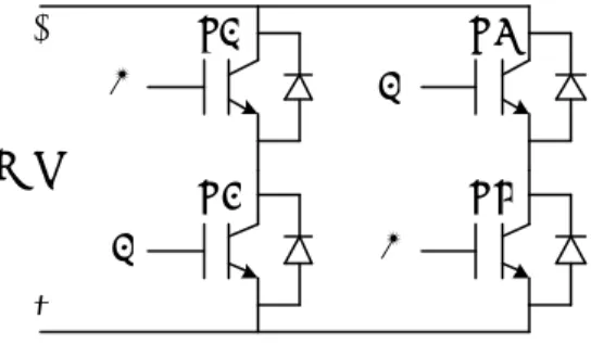
The voltage deviations can be examined form single phase of the PWM voltage inverter. Show in fig. 1. This consists of upper and lower power devices T1,T4 and T2,T3 that are connected between the positive and negative of the DC power supply.
Fig. 1 Single phase PWM inverter.
The power device switching sequence as T1 and T4 and T2 and T3 work opposite to each other. For example when T1 and T4 is turning off and T2 and T3 turning on, This caused a situation or a time when both power devices ceased to conduct. During dead time the output appears to be floating. The reference voltage might be delayed by the dead time.
Fig. 2 Dead-Time compensation signal.
The A and B signal are the output of the comparator circuit. The signal fed to lock out circuit for preventing the short-circuit condition of the A’ and B’ signal respectively. The A” and B” signal are the output of the compensation Dead-Time circuit. The A” signal an increase in pulse time as compared to the A signal pulse time is similar.
Compensation of Dead-Time in PWM Voltage Inverters
Nitipong Somchaiwong*, Ekkachai Chaidee*
* Department of Electrical, Faculty of Engineering, Rajamangala University of Technology Lanna, Chiangrai Campus, Chiangrai, 57120 Thailand
(Tel : 66-5-372-9600; E-mail: [email protected])
Abstract: Dead-Time is necessary to prevent the shot circuit of the full bridge inverters in pulse width modulation. However the
output voltage deviations is the result of the Dead-Time that decrease power from the out put voltage inverters. This paper presents the method that compensate power output voltage inverters loss in Dead-Time circuit for DC Motor Drives with full bridge voltage inverters. The compensation of Dead-Time method is a sample and a low-cost solution. The comparison between the test results and simulation by MATLAB &SIMULINK under the same condition is similar.
Keywords: Dead-Time, PWM, Compensation, Voltage Distortion
T 2T
A
B
'A
'B
''A
''B
t V PWM Time Dead -time Dead on Compensati -TICCAS2005 June 2-5, KINTEX, Gyeonggi-Do, Korea
ICCAS2005 June 2 -5, KINTEX, Gyeonggi-Do, Korea
3. PRINCIPLE OF DC MOTOR DRIVER DESIGN
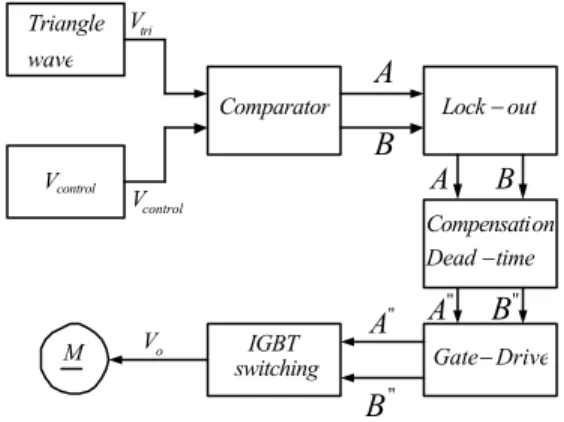
The Fig. 3. and Fig. 4. show the block diagram of DC - Motor driver. Which consist of 2 main circuit.
1. Control Circuit. 2. Power Circuit.
Fig. 3 Block diagram of DC-Motor drive
Fig. 4 Block diagram of DC-Motor drive used MATLAB&SIMULINK
3.1 The control circuit.
The control circuit generates the
V
control signal forcontrol the electronic switch is show in Fig. 5.
Fig. 5 The
V
control signal.The
V
control signal is modulated with the triangle signal for generate the Pulse Width Modulation signal. The triangle signal and the PWM signal is show in Fig. 6. and Fig. 7.Fig. 6 The triangle signal.
Fig. 7 The PWM signal.
Fig. 8 The PWM signal used MATLAB&SIMULINK The PWM signal will be lock out the signal for preventing the short-circuit condition. The output signal of the lock out circuit is shown in the Fig. 9.
wave Triangle
control
V
Comparator Lock-out
time Dead on Compensati -Drive Gate -IGBT switching M tri V control V
A
B
'A
B
' " A "B
o V "A
B
"818
ICCAS2005 June 2 -5, KINTEX, Gyeonggi-Do, Korea
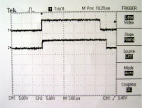
Fig. 9 The output signal of the lock out circuit. The 1 signal is the output of the comparator circuit. The 2 signal is the output of the lock out circuit.
Before the lock out signal is fed to the driver circuit, it will compensate the signal. The output signal of the compensation circuit is shown in the Fig. 10. and Fig. 11. respectively.
Fig. 10 The output signal of the compensation circuit. The 1 signal is the output of the lock out circuit. The 2 signal is the output of the compensation circuit.
Fig. 11 The comparator signal and the compensation signal. The 1 signal is the output of the comparator circuit. The 2 signal is the output of the compensation circuit.
Fig. 12 The signal before fed to power circuit.
The top signal is the output of the comparator circuit. The
middle signal is the output of the lock out circuit. The bottom signal is the output of the compensation circuit.
3.2 The power circuit.
The power circuit that control the input power of the motor, depends on the PWM signal. The PWM signal has a 1 signal for single phase full bridge module part No. IRG4PC50UD. The power circuit is shown in the Fig. 13.
Fig. 13 The power circuit.
The power circuit consists of 4 modules of IGBT and connects in parallel, which is driven by PWM signal.
4. THE EXPERRIMENTAL RESULT The experiment is performed on DC motor type 2 HP 1750 RPM. 190 volt. The digital storage oscilloscope is use for recording the electrical signals. The speed response in clockwise (CW) and counter – clockwise (CCW) as shown in table 1 and 2 .
The motor speed will be increasing when the input voltage is applied to the motor. The speed response to the motor is linearity with the supply voltage.
The motor speed in CW and CCW of the compensation dead time are 2.3 percent more than the motor sp eed in CW and CCW of the no compensation dead time.
Additionally, From Fig. 2. show the phase shift in compensation circuit can change the speed response in CW
and CCW. This is because the
V
control is increasing T voltper pulse.
Vdc
+
-''A
''A
''B
''B
1
T
2
T
3
T
4
T
M
819
ICCAS2005 June 2 -5, KINTEX, Gyeonggi-Do, Korea
Table 1 The motor speed in clockwise.
motor speed(RPM) a
M
no compensation compensation 10% 0 128 20% 118 363 30% 335 614 40% 575 853 50% 780 1,051 60% 1,044 1,322 70% 1,242 1,537 80% 1,495 1,785 90% 1,730 2,171 100% 2,034 2,176Table 2 The motor speed in counter - clockwise. motor speed(RPM) a
M
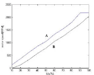
no compensation compensation 10% 0 134 20% 122 371 30% 339 620 40% 579 859 50% 788 1,055 60% 1,052 1,329 70% 1,247 1,540 80% 1,495 1,791 90% 1,734 2,172 100% 2,035 2,179Fig. 14 The speed response of the motor clockwise. The A show the speed response of the compensation dead – time. The B show the speed response of the no compensation dead – time.
Fig. 15 The speed response of the motor counter - clockwise. The A show the speed response of the compensation dead – time. The B show the speed response of the no compensation dead – time.
From Fig. 14. and Fig. 15. show speed response of the DC motor to vary the input voltage. The responses show that speed of the motor depends on the input voltage.
5. SUMARY
This paper presents the technique to apply the simulation result of the compensation Dead-Time in PWM voltage inverter for designing the DC Motor driver circuit. The simulation result can be known the response of the system. This paper designs the control circuit and the power circuit with the simulation result. The experimental results of the driver system are similarly witch the simulation result.
REFERENCES
[1] J.M.D. Murphy and F.G. Turnbull, “Power Electric Control of AC Motor,” Pergamon Rpess, 1988.
[2] P.C. Krause,“Analysis of Electric Machinery,” McGraw -Hill Book company, 1987.
[3] R.Krishnan, “Electric Motor Drives Modeling,. Analysis, and Control,” Virginia Tech, Blacksburg-VA, 2001. [4] D. Leggate and R.Kerkman, “Pulse base time
compensator for PWM Voltage Inverters,” in IEEE IECON Conf.Rec., pp. 474-481, 1995.
[5] J. Kimball and P.T. Krein,”Real time optimization of dead time for motor control inverter,” in IEEE PESC, st. Louis, MO, pp. 597-600, 1997.