Manuscript received Apr. 18, 2017; accepted Aug. 1, 2017 Dept. of Radio Science and Engineering, Kwangwoon University, Seoul, Korea
E-mail : [email protected]
Initial Frequency Preset Technique for Fast Locking
Fractional-N PLL Synthesizers
Jihoon Sohn and Hyunchol Shin
Abstract—This paper presents a fast locking
technique for a fractional-N PLL frequency synthesizer. The technique directly measures KVCO on a chip, computes the VCO’s target tuning voltage for a given target frequency, and directly sets the loop filter voltage to the target voltage before the PLL begins the normal closed-loop locking process. The closed-loop lock time is significantly minimized because the initial frequency of the VCO are put very close to the desired final target value. The proposed technique is realized and designed for a 4.3-5.3 GHz fractional-N synthesizer in 65 nm CMOS and successfully verified through extensive simulations. The lock time is less than 12.8 ms over the entire tuning range. Simulation verifications demonstrate that the proposed method is very effective in reducing the synthesizer lock time.
Index Terms—Lock time, initial frequency preset
method, PLL, frequency synthesizer, CMOS
I.
I
NTRODUCTIONLow-power wireless connectivity capability such as Bluetooth, Zigbee, and other proprietary technique is essential for the internet-of-things (IoT) applications. Low-power low-voltage complementary metal-oxide-semiconductor (CMOS) RF transceivers are highly needed for these applications [1-4]. It is known that the average power consumption for IoT’s wireless
communication can be significantly minimized by heavily controlling the active and sleep duty cycles of RF transceivers, which is usually referred to as duty-cycling technique. For efficient duty-cycling, fast start-up of RF transceiver is crucial for minimizing the average power consumption [5]. Since the RF transceiver’s start-up time is mostly consumed by the locking process of the synthesizers, reducing the phase-locked loop (PLL) lock time becomes more crucial for IoT RF transceivers.
PLL lock time is approximately given by [6]
1 ln step lock tol LBW f T f w æ ö » ç ÷ è ø (1)
where wLBW, fstep, and ftol are the loop bandwidth, the
frequency step difference between the start (initial) and final (target) frequencies, and the tolerance of frequency error within which a PLL can be seen fully locked, respectively. As ftol is given according to the system
requirements, the lock time Tlock can be reduced by either
increasing wLBW or decreasing fstep.
Based on this viewpoint, previous fast locking techniques typically include two approaches: the bandwidth switching method and the initial frequency preset method. The bandwidth switching method temporarily widens the loop bandwidth during the locking process, and returns it to the original narrow condition after the locking has been completed to reduce phase noise and reference spur [7, 8]. Bandwidth widening is usually achieved by increasing the charge pump current. The limitation of this method is that the phase offset between the reference and voltage-controlled oscillator (VCO) clocks is inevitably perturbed when the charge-pump current switches back and forth. Such phase
perturbation can easily perturb the PLL lock condition, which then delays the lock time again. An adaptive phase compensation technique has been proposed to minimize such perturbation [9]. However, due to the dynamic control of the dividing ratio during the locking process, it was not suitable for the DS fractional-N synthesizer.
The initial frequency preset method minimizes fstep by
presetting the initial frequency as close as possible to the target frequency [10, 11]. This method relies on the precise control of the VCO frequency. However, due to the process, temperature, and voltage variations, the VCO frequency tuning characteristic can deviate from the original design. Hence, the initial frequency preset error cannot be avoided in practice. As a result, the lock time improvement effect can be significantly degraded.
This work presents an improved fast locking technique based on a more robust and precise initial frequency preset method. The proposed method overcomes the fundamental limitations of the previous preset method. Section II describes the operation principle of the proposed technique, and Section III presents the design details. Simulation results and verifications are presented in Section IV, and finally, conclusions are given in Section V.
II.
I
NITIALF
REQUENCYP
RESETM
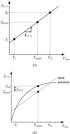
ETHOD 1. Operating PrincipleThe proposed initial frequency preset method is devised by assuming linear voltage-to-frequency tuning characteristics in VCO. Fig. 1(a) shows that the VCO frequency is linearly dependent on Vtune, in which the
VCO gain KVCO is determined by the slope. Assuming
two points (VL vs. fL, and VH vs. fH) are known for a VCO
and the tuning curve is perfectly linear between the two points, the target voltage Vtarget for a target frequency
ftarget can be computed by
target target ( ) L H L L H L f f V V V V f f -= ´ - + - (2)
where the two frequencies fH and fL are the frequencies
when the tuning voltages Vtune are VH and VL, respectively.
In this method, we directly measure the VCO frequencies
fH and fL on a chip, then calculate Vtarget with respect to a
given ftarget by using the acquired data, and finally preset
Vtune to the computed Vtarget. Then, when the PLL begins
its closed-loop locking process, the VCO is ready to produce almost the same frequency as the final target frequency ftarget. Since the VCO’s initial frequency is
close to ftarget, the PLL can reach the locked state very
quickly. It should be noted that, in the previous methods [10, 11], the frequency preset is performed without the knowledge of the real KVCO value, and by only assuming
the designed KVCO value. Meanwhile, the proposed
method performs the frequency preset by using the on-chip directly measured KVCO, which guarantees the
accuracy and robustness of the frequency preset process. One of the practical limitations of this method is the frequency error. In practice, the VCO tuning characteristic curve will not be perfectly linear and can also vary with the process, voltage, and temperature. When the tuning curves are not perfectly linear as depicted in Fig. 1(b), the required target frequency ftarget
(a)
(b)
Fig. 1. VCO frequency tuning characteristic according to (a) ideal KVCO, (b) practical KVCO.
and the resulting output frequency fout will inevitably
deviate by the amount of the frequency error ferror. Such
frequency error ferror will degrade the fast locking effect.
Therefore, the amount of ferror needs to be well controlled
within a certain range to successfully achieve the lock time improvement effect.
Another practical limitation of the proposed method is the initial phase error. Even when ferror is zero, the initial
phase error between the divided VCO signal and the reference clock signal can degrade the lock time because PLL can be only locked when both the frequency and phase are aligned. Thus, to ensure the initial phase error is zero, the initial phase alignment is also crucial for the fast locking technique.
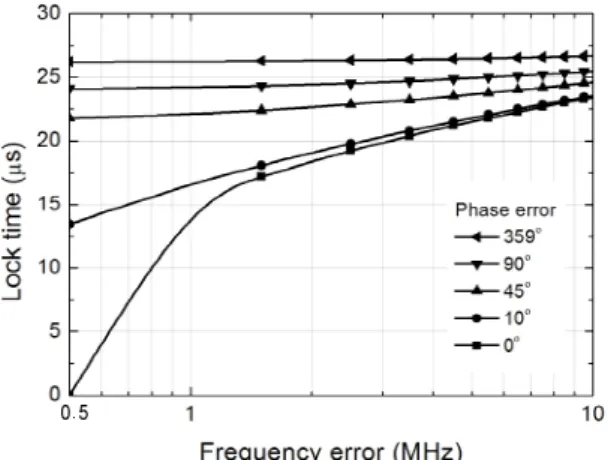
We investigated the effects of the frequency and phase error on the lock time, and the results are shown in Fig. 2. The results are obtained by behavioral simulations for a PLL with VCO frequency of 4880 MHz, KVCO of 40
MHz/V, reference frequency of 40 MHz, loop bandwidth of 50 kHz, and charge pump current of 100 mA.
Note that the simulation investigation in Fig. 2 is carried out up to 10-MHz frequency error, which is sufficient to see the lock time dependency on the frequency error. The maximum frequency error is given by the resolution of the VCO frequency coarse tuning process [16]. For example, in a typical RF synthesizer design, let us assume the VCO tuning range is 1000 MHz, which is then covered by 6-bit switched capacitor array. Then, the resolution of the VCO frequency coarse tuning is 15.6 MHz. Thus, in typical RF synthesizer, the initial
frequency error will be no more than about 10 MHz. As can be seen in Fig. 2, the lock time is reduced as the frequency and phase error decrease. For example, for the lock time of 20 μs or less, the initial frequency and phase error must be less than 2.5 MHz and 10°, respectively.
2. Architecture
Fig. 3 shows the architecture of the proposed initial frequency preset circuit. Note that the circuit operates in an open loop. The frequency-to-digital converter (FDC) converts the VCO frequency to a digital value
kIFP·fVCO/fREF, where the counting index kIFP indicates the
number of fREF periods that are consumed for counting
the VCO signal fVCO. When the circuit starts, the voltage
presetter sequentially applies VL and VH to Vtune, and the
FDC acquires fL and fH in digital values. When ftarget is
given by a user, the digital values of fH, fL, VH, and VL are
used to compute Vtarget according to (2). Finally, the
computed Vtarget is applies to Vtune by the voltage presetter
so that the initial VCO frequency is readily set to ftarget.
After the completion of the open-loop initial frequency preset process, the PLL starts the closed-loop locking process.
3. Residual Frequency Error due to FDC
Since FDC counts the VCO frequency in a limited time kIFP/fREF, a certain amount of error in the frequency
counting process cannot be avoided. Two causes for the frequency error can be considered: the quantization error and the initial phase uncertainty error. The quantization error can be as large as half the reference clock period, and the phase uncertainty error can be as large as one Fig. 2. Lock time with respect to the frequency error and
phase error. (Lock time is measured with 40 ppm accuracy when fVCO is 4880 MHz, fREF is 40 MHz, and the loop bandwidth is 50 kHz).
reference clock period [12]. Hence, the worst-case frequency error caused by the FDC is given by
_ 1.5 REF error FDC IFP f f k = ´ . (3)
Fig. 4 shows a plot of ferror_FDC with respect to kIFP
when fREF is 40 MHz. As can be seen, the frequency error
decreases as kIFP increases. For example, for the
frequency error below 1 MHz, kIFP must be greater than
60.
III.
PLL
S
YNTHESIZERC
IRCUITD
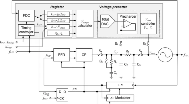
ESIGN The proposed fast locking circuit is realized with a DS fractional-N PLL synthesizer in 65 nm CMOS. Fig. 5 shows a block diagram of the PLL. The loop filter is a third-order passive type. The reference clock fREF is 40MHz. The LC VCO covers 4.3 – 5.3 GHz by employing a 6-bit capacitor bank. The DS modulator is a MASH 1-1-1 type with 20-bit resolution. The charge pump employs the servo-loop technique by using a rail-to-rail opamp for the current matching [13]. The initial frequency preset block in Fig. 3 is realized as shown in Fig. 5. As the initial frequency preset process starts, the PLL is configured to an open loop, with S2 closed and
S1,3,4,5 open. Then, the Vtune controller sequentially sets
Vtune to VL and VH to ensure that FDC can acquire fL and
fH, respectively. The target frequency ftarget is converted to
its digital value of kIFP·Ntarget, where Ntarget represents the
total division ratio for the target frequency. The Vtarget
calculator then computes the Vtarget as a digital value by
utilizing the acquired data, including fL, fH, VL, VH, and
kIFP·Ntarget.. This digital Vtarget is converted to an analog
voltage via the 10-bit digital-to-analog converter (DAC). Then, S1 and S3 are closed and the precharger sets the
loop filter voltage VLF to Vtarget. Note that the charging
time of the precharger is minimized by shorting out the
Fig. 5. DS fractional-N PLL synthesizer with the initial frequency presetting circuit. Fig. 4. Frequency error due to the frequency-to-digital counter.
resistor R1 by closing S3 and increasing the current
driving capability at the output. Meanwhile, the Vtune
controller charging time is not problematic because the load capacitance seen at the Vtune node is relatively small
compared to the loop filter capacitors C1 and C2.
Fig. 6 shows the timing diagram of the entire locking process. The initial frequency preset process operates in two steps during tIFP and tcharge. In the first tIFP period, the
VCO frequency is measured and Vtarget is calculated. In
the subsequent tcharge period, VLF is charged to Vtarget.
After the VLF is fully charged to Vtarget, S1-3 are open and
S4-5 are shorted. The PLL then begins the closed-loop
locking process.
As explained for Fig. 2, the initial phase error between
fREF and fDIV must be maintained to be less than 10o
before the closed loop locking begins. The initial phase error can be removed by employing the D flip-flop shown in Fig. 5, which is used to synchronize the PFD and the feedback divider output signals. After the completion of the initial frequency preset operation, Flag signal is generated. The Flag signal subsequently generates the PLL enable signal EN that is synchronized to fREF. The charge pump, PFD, feedback divider, and
delta-sigma modulator of the PLL begin operations at the same time as this EN signal. Therefore, the PFD and frequency divider output signals are successfully synchronized with the first rising edge of fREF.
Even after this initial synchronization, the phase error can occur again at the next rising edge as shown in Fig. 7.
This is attributed to two reasons. First, the initial VCO phase is unknown, which can lead to a phase error equivalent to one fVCO period at maximum. Second, the
instantaneous feedback division ratio N differs from the desired fractional value, which also can lead to a phase error equivalent to half the fVCO period at maximum. Thus,
the worst-case phase error due to the two effects will be given by VCO 1.5 2 error REF T T p ´ F = ´ (4)
For example, when fVCO is 4.3 GHz and fREF is 40 MHz,
the worst-case initial phase error will be 5o, which is
acceptable considering Fig. 2.
1. VCO
Fig. 8 shows the VCO schematic, which is a complementary cross-coupled negative-gm type [14]. The
frequency tuning range is 4.3 to 5.3 GHz. An on-chip RC low-pass filter is used to suppress 1/f and thermal noise coupling. The tank inductor is 1.5 nH and a 6-bit binary weighted capacitor bank is implemented using a 40 fF metal-insulator-metal (MIM) unit capacitor. As shown in Fig. 1(b), a non-constant KVCO can cause the undesirable
frequency error ferror. Thus, in this design, the varactor
averaging technique with three off-biased varactors [15] is adopted to linearize the tuning curves against the tuning voltage. The simulation results of the frequency error ferror for the designed VCO are given in Fig. 9.
These results verify that the error ranges for all of the 64 tuning curves with respect to the tuning voltage are less than 1.25 MHz, which is acceptable when considering Fig. 2.
Fig. 6. Timing diagram of the locking process.
Flag fREF fDIV EN TREF TVCO×N Φerror
2. DAC and Precharger
The DAC and precharger generate the target voltage
Vtarget for ftarget, which is then fed to Vtune to preset the
voltage to Vtarget. Thus, any voltage error of the DAC and
precharger circuits will directly affect the frequency error
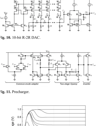
ferror. The DAC is designed as a 10-bit R-2R type to meet
the accuracy requirement. Fig. 10 shows the DAC circuit followed by a non-inverting buffer amplifier. The full scale of the output signal is almost rail-to-rail, and simulations show that the integral nonlinearity (INL) of DAC is -0.25 to +0.63 LSB.
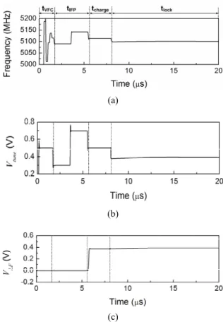
Fig. 11 shows the precharger circuit. It consists of a common-mode adapter, a two-stage amplifier, and an inverter. The input common-mode range of the
precharger needs to cover the full range of the Vtune of the
VCO between 0.3 and 0.7 V. Thus, the precharger should almost have a rail-to-rail common mode range at the input in order to accept the DAC output voltage. When the common mode level of VINP and VINN is higher than
VREF, where VREF is set at the maximum input common
mode level of the two-stage operation amplifier, the common-mode adapter lowers the common-mode level at M11 and M12 by subtracting the IR (current times
resistance) drop from the VIN common-mode level. The
final inverter buffer operates as a class AB amplifier so that the current driving capability is significantly increased. Fig. 12 shows the settling behavior of the designed precharger with a 2.3 nF load capacitor. As can be seen, the precharger can charge the loop filter to any voltage below the 1-V supply within 1 ms.
Fig. 8. VCO.
Fig. 9. Frequency error induced by nonlinear VCO tuning characteristic.
Fig. 10. 10-bit R-2R DAC.
Fig. 11. Precharger.
IV.
R
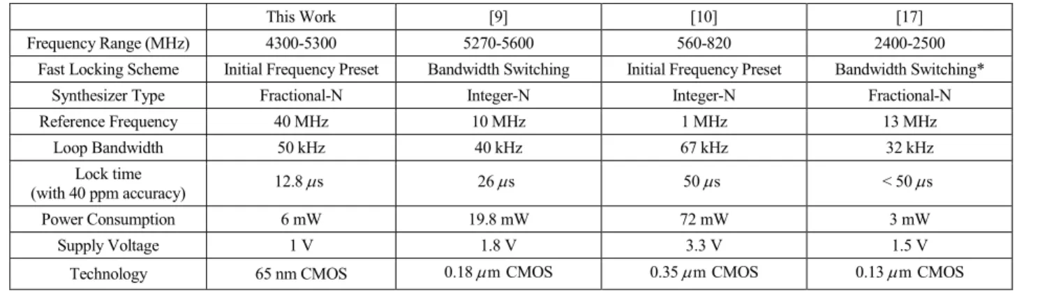
ESULTSThe proposed PLL is designed in a 65nm CMOS. The reference frequency is 40 MHz. Fig. 13 shows the layout of the proposed PLL. The dimensions are 1300 × 1000 mm2, including the pad frame. In order to verify the proposed initial frequency presetting method, the time-domain locking simulations are extensively performed and the results are shown in Fig. 14 and 15. The locking simulations are performed for two target frequencies, one at a high-end frequency (= 5100 MHz) and the other at a low-end frequency (= 4425 MHz). To minimize the initial frequency preset error, kIFP and kcharge are set to 64 and 80,
respectively. Fig. 14(a)-(c) show the PLL output frequency, the Vtune voltage, and the VLF voltage, respectively. At the
beginning, the PLL is set to open loop and begins to perform the VCO frequency calibration process as described in [16] during tVFC, which results in finding an
optimum VCO capbank code closest to ftarget. Then, the
initial frequency preset process is carried out during tIFP,
and finally the VLF is charged to the computed Vtarget during
tcharge. The entire process is completed in 8 ms. Then, the
PLL loop is closed and the normal closed-loop locking process begins. As shown in Fig. 14, after the closed-loop locking process begins at 8 ms, the VCO frequency, Vtune,
and VLF do not show significant changes because they are
already put very close to the final target values. Such small changes due to the use of the proposed initial frequency preset method successfully ensure fast locking. Fig. 15 verifies the locking process at 4425 MHz by showing the VCO frequency. It also demonstrates that the proposed method is successfully operational and useful for reducing the lock time.
Fig. 16 compares the lock time for the conventional
and proposed PLLs. We assume the initial coarse calibration process is finished at 8 ms for both PLL’s, from which the closed-loop locking process begins. For the conventional PLL, the initial frequency is found to be 5114 MHz, which is given when Vtune is set to a half VDD.
Since the target frequency is 5100 MHz, the initial frequency offset is given by 14 MHz, and as implied in Fig. 2, the frequency goes through large fluctuations during locking, and the lock time with 40 ppm accuracy is 23 μs. By contrast, the PLL with the proposed method sets the initial frequency to 5098 MHz, which only 2 MHz away from the target frequency. Thus, the Fig. 13. Chip layout.
(a)
(b)
(c)
Fig. 14. Time-domain locking process of the PLL with the initial frequency preset method (Target frequency is 5100 MHz) (a) Output frequency, (b) Vtune, (c) VLF.
Fig. 15 Transient locking process of PLL with the initial frequency preset method at 4425 MHz.
frequency quickly approaches to the final target frequency. With the frequency error of 40 ppm, the lock time of the proposed PLL is found to be 12.8 μs, which is only 55 % of the conventional PLL.
Table 1 compares the proposed methods with prior methods. With a similar loop bandwidth, the proposed technique demonstrates the fastest lock time.
V.
C
ONCLUSIONSA robust initial frequency preset technique is presented for fast-locking fractional-N PLL synthesizers. Through on-chip frequency and KVCO measurement, the initial
frequency presetting circuit finds the precise target loop filter voltage with small frequency error, and significantly reduces the lock time.
A
CKNOWLEDGMENTSThis work was supported by the Institute for Information and Communications Technology Promotion
(IITP) grant funded by the Korea Government (MSIT) under “Development of Ultra-Low-Power Dual/Wide-Band MICS/BAN Transceiver for Capsule Endoscopy (2016-0-00111)”, “Development of Intelligent Semicon- ductor Core Technologies for IoT Devices based on Harvest Energy (2016-0-00421)”, and “University ITRC program (2012-0-00641)”.
R
EFERENCES[1] A. Wong, M. Dawkins, G. Devita, N. Kasparidis, A. Katsiamis, O. King, F. Lauria, L. Schiff, A. Burdett, “A 1V 5mA Multimode IEEE 802.15.6/Bluetooth Low-Energy WBAN Transceiver for Biotelemetry Application,” in IEEE Int. Solid-State Circuits Conf.
Dig., Feb. 2013, pp. 300-302.
[2] J. Masuch, M. Delgado-Restituto, “A 1.1-mW-RX 81.4-dBm Sensitivity CMOS Transceiver for Bluetooth Low Energy,” IEEE Tran. Microw. Theory
Tech., vol. 61, no. 4, pp. 1660-1673, Apr. 2013.
[3] Y. Liu, X. Huang, M. Vidojkovic, A. Ba, P. Harpe, G. Dolmans, H. d. Groot, “A 1.9nj/b 2.4GHz Multistandard(Bluetooth Low Energy/Zigbee/IEEE 802.15.6) Transceiver for Personal/Body-Area Networks,” in IEEE Int. Solid-State Circuits Conf.
Dig., Feb. 2013, pp. 446-448.
[4] C. Bachmann, G. V. Schaik, B. Busze, M. Konijnenburg, Y. Zhang, J. Stuyt, M. Ashouei, G. Dolmans, T. Gemmeke, H. d. Groot “0.74V 200mW Multi-Standard Transceiver Digital Baseband in 40nm LP-CMOS for 2.4GHz Bluetooth Smart/Zigbee/IEEE 802.15.6 Personal Area Networks,” in IEEE Int. Solid-State Circuits
Conf. Dig., Feb. 2014, pp. 186-188.
Table 1. Performance Comparison
This Work [9] [10] [17]
Frequency Range (MHz) 4300-5300 5270-5600 560-820 2400-2500
Fast Locking Scheme Initial Frequency Preset Bandwidth Switching Initial Frequency Preset Bandwidth Switching*
Synthesizer Type Fractional-N Integer-N Integer-N Fractional-N
Reference Frequency 40 MHz 10 MHz 1 MHz 13 MHz Loop Bandwidth 50 kHz 40 kHz 67 kHz 32 kHz Lock time (with 40 ppm accuracy) 12.8m s 26m s 50m s < 50m s Power Consumption 6 mW 19.8 mW 72 mW 3 mW Supply Voltage 1 V 1.8 V 3.3 V 1.5 V
Technology 65 nm CMOS 0.18mmCMOS 0.35mmCMOS 0.13mmCMOS
* Implemented in all-digital PLL 6 12 18 24 30 36 5090 5100 5110 5120
Conventional without the initial frequency preset method Proposed with the initial frequency preset method
F re q u e n cy ( M H z) Time (ms)
Fig. 16. Locking behaviors with and without fast locking technique.
[5] F. Pengg, D. Barras, M. Kucera, N. Scolari, A. Vouilloz, “A Low Power Miniaturized 1.95mm2 Fully Integrated Trasnsceiver with fastPLL Mode for IEEE 802.15.4/Bluetooth Smart and Proprietary 2.4GHz Applications,” in Proc. IEEE Radio Freq.
Integr. Circuit Symp., Jun. 2013, pp. 71-74.
[6] C. Vaucher, “An Adaptive PLL Tuning System Architecture Combining High Spectral Purity and Fast Settling Time,” IEEE J. of Solid-State Circuits, vol. 35, no. 4, pp. 490-502, Apr. 2000.
[7] Y. Tang, M. Ismail, S. Bibyk, “A new fast-settling gearshift adaptive PLL to extend loop bandwidth enhancement in frequency synthesizers,”in Proc.
IEEE Int. Symp. on Circuits and Systems, May
2002, pp 787-790.
[8] K. Woo, Y. Liu, E, Nam, D. Ham, “Fast-Lock Hybrid PLL Combining Fractional-N and Integer-N Modes of Differing Bandwidths,”IEEE J. of Solid-State Circuits, vol. 43, no. 2, pp 379-389, Feb. 2008.
[9] W. –H. Chiu, Y. -H. Huang, T. -H. Lin, “A Dynamic Phase Error Compensation Technique for Fast-Locking Phase-Locked Loops,” IEEE J. of Solid-State
Circuits, vol. 45, no. 6, pp 1137-1149, Jun. 2010.
[10] X. Kuang, N. Wu, “A Fast-Settling Frequency Synthesizer with Direct Frequency Presetting,”
IEEE Int. Solid-State Circuits Conf. Dig., pp.
741-750, Feb. 2006.
[11] X. Yan, X. Kuang, N. Wu, “A Smart Frequency Presetting Technique for Fast Lock-in LC-PLL Frequency Synthesizer,” IEEE Int. Symp. on
Circuits and Systems, pp.1525-1528, May, 2009.
[12] J. Zhou, W. Li, D. Huang, c. Lian, N. Li, J. Ren, “A Dual-Mode VCO based Low-Power Synthesizer with Optimized Automatic Frequency Calibration for Software-Defined Radio,” IEEE Int. Symp. on
Circuits and Systems, pp.1145-1148, May 2011.
[13] J. Sohn and H. Shin, “A CMOS charge pump circuit with short turn-on time for low-spur PLL synthesizers,” J. of Semiconductor Tech. and
Science, vol. 16, no. 6, pp. 873-879, Dec. 2016.
[14] J. Shin, J. Kim, S. Kim, H. Shin, “A Delta-Sigma Fractional-N Frequency Synthesizer for Quad-Band Multi-Standard Mobile Broadcasting Tuners 0.18-mm CMOS,” J. of Semiconductor Tech. and
Science, vol. 7, no. 4, pp. 267-273, Dec. 2007.
[15] J. Mira, T. Divel, S. Ramet, J. -B Begueret, and Y. Deval, “Distributed MOS Varactor Biasing for
VCO Gain Equalization in 0.13 mm CMOS Technology,” in IEEE Radio Freq. Integr. Circuit
Symp., May 2004, pp. 131-134.
[16] J. Shin and H. Shin, “A 1.9-3.8 GHz DS Fractional-N PLL Frequency Synthesizer with Fast Auto-Calibration of Loop Bandwidth and VCO Frequeny,” IEEE J. of Solid-State Circuits, vol. 47, no. 3, pp. 665-675, Mar. 2012.
[17] R. B. Staszewski and P. T. Balsara, “All-Digital PLL With Ultra Fast Settling,” IEEE Tran. Circuits
and Systems-II: Exp. Briefs, vol. 54, no. 2, pp.
181-185, Feb. 2007
Jihoon Sohn was born in Korea in 1984. He received B.S. from Kwang- woon University in 2010, and is currently working toward Ph.D. at the same university. His research is focused on the PLL frequency synth- esizers and analog circuits in CMOS.
Hyunchol Shin received the B.S., M.S., and Ph.D. degrees in electrical engineering from the Korea Advanced Institute of Science and Technology (KAIST), Daejeon, Korea, in 1991, 1993, and 1998, respectively. During his Ph.D., he held an internship as a Doktorand at the Daimler-Benz Research Center, Ulm, Germany. Upon completion of the Ph.D, he worked at several research institutions and companies, including Samsung Electronics, Korea, University of California at Los Angeles, CA., USA, and Qualcomm, San Diego, CA, USA, where he had been involved in RF/analog circuit design for wireless communications. Since 2003, he has been with Kwangwoon University, Seoul, Korea, where he is currently a Professor with the Department of Electronics Convergence Engineering. From 2010 to 2011, he took his sabbatical leave with Qualcomm, San Diego, CA, USA. He has coauthored over 80 journal and conference papers. He holds over 30 patents in the field of RF/analog circuit design. His research interests focus on CMOS RF/analog/microwave circuits and phase-locked loop (PLL) frequency synthesizers. Prof. Shin has served on Technical Program Committees of several IEEE conferences such as the International Solid-State Circuits Conference (ISSCC), the VLSI Circuit Symposium (VLSI), the Asian Solid-State Circuit Conference (A-SSCC), the Midwest Symposium on Circuits and Systems (MWCAS), and the International System-on-Chip Conference (ISOCC).
![Fig. 8 shows the VCO schematic, which is a complementary cross-coupled negative-g m type [14]](https://thumb-ap.123doks.com/thumbv2/123dokinfo/4885333.35776/5.892.107.398.113.425/fig-shows-vco-schematic-complementary-cross-coupled-negative.webp)