Microcavity effect using nanoparticles to
enhance the efficiency of organic light-emitting
diodes
Jun Hee Han,1 Do-Hong Kim,1 and Kyung Cheol Choi1,*
1Department of Electrical Engineering, KAIST, Daejeon, 305-701, South Korea
Abstract: In this paper, in contrast with previously reported approaches, we
suggest exploiting a microcavity effect using nanoparticles to improve the optical efficiency of organic light-emitting diodes (OLED). The method to input the nanoparticles inside the OLED device is simple and cost effective by virtue of employing a solution process using a spin coating fabrication method. Titanium dioxide (TiO2) nanoparticles were used to improve the
reflection by its high refractive index. In tandem with optimized heights of the organic layers, the increased light reflectance at the anode side, which includes the TiO2 nanoparticle layer, improved the optical efficiency of the
OLED device via the microcavity effect. In order to prove that the enhancement of the optical efficiency was due to an enhanced microcavity
effect caused by TiO2 nanoparticles, a microcavity simulation was
conducted. The electrical characteristics were not affected by the nanoparticles and a clear pixel image was maintained. The results in this paper show that a nanoparticle based microcavity effect can be exploited to enhance the optical efficiency of OLEDs.
©2015 Optical Society of America
OCIS codes: (230.3670) Light-emitting diodes; (140.3945) Microcavities; (050.2230) Fabry-Perot; (220.4241) Nanostructure fabrication.
References and links
1. S. R. Forrest, D. D. C. Bradley, and M. E. Thompson, “Measuring the efficiency of organic light-emitting devices,” Adv. Mater. 15(13), 1043–1048 (2003).
2. R. Meerheim, M. Furno, S. Hofmann, B. Lüssem, and K. Leo, “Quantification of energy loss mechanisms in organic light-emitting diodes,” Appl. Phys. Lett. 97(25), 253305 (2010).
3. K. Hong and J. Lee, “Review paper: Recent developments in light extraction technologies of organic light emitting diodes,” Electron. Mater. Lett. 7(2), 77–91 (2011).
4. K. Saxena, V. K. Jain, and D. S. Mehta, “A review on the light extraction techniques in organic electroluminescent devices,” Opt. Mater. 32(1), 221–233 (2009).
5. L. H. Smith, J. E. Wasey, I. D. W. Samuel, and W. L. Barnes, “Light out-coupling efficiencies of organic light-emitting diode structures and the effect of photoluminescence quantum yield,” Adv. Funct. Mater. 15(11), 1839– 1844 (2005).
6. C. Adachi, M. Baldo, M. E. Thompson, and S. R. Forrest, “Nearly 100% internal phosphorescence efficiency in an organic light-emitting device,” J. Appl. Phys. 90(10), 5048 (2001).
7. S. Tokito, T. Iijima, Y. Suzuri, H. Kita, T. Tsuzuki, and F. Sato, “Confinement of triplet energy on phosphorescent molecules for highly-efficient organic blue-light-emitting devices,” Appl. Phys. Lett. 83(3), 569–571 (2003).
8. Y. Sun and S. R. Forrest, “Enhanced light out-coupling of organic light-emitting devices using embedded low-index grids,” Nat. Photonics 2(8), 483–487 (2008).
9. J. Kim and K. Choi, “Improvement in outcoupling efficiency and image blur of organic light-emitting diodes by using imprinted microlens arrays,” J. Disp. Technol. 7(7), 377–381 (2011).
10. S. Möller and S. R. Forrest, “Improved light out-coupling in organic light emitting diodes employing ordered microlens arrays,” J. Appl. Phys. 91(5), 3324 (2002).
11. S. Jeon, J.-W. Kang, H.-D. Park, J.-J. Kim, J. R. Youn, J. Shim, J. Jeong, D.-G. Choi, K.-D. Kim, A. O. Altun, S.-H. Kim, and Y.-H. Lee, “Ultraviolet nanoimprinted polymer nanostructure for organic light emitting diode application,” Appl. Phys. Lett. 92(22), 223307 (2008).
12. Y.-C. Kim, S.-H. Cho, Y.-W. Song, Y.-J. Lee, Y.-H. Lee, and Y. R. Do, “Planarized SiN[sub x]/spin-on-glass photonic crystal organic light-emitting diodes,” Appl. Phys. Lett. 89(17), 173502 (2006).
13. D.-Y. Kim, C. S. Choi, J. Y. Kim, D. H. Kim, and K. C. Choi, “Phosphorescent transparent organic light-emitting diodes with enhanced outcoupling efficiency: Reduction of surface plasmon losses,” Org. Electron. 15(6), 1222–1228 (2014).
14. J. Y. Kim, C. S. Choi, W. H. Kim, D. Y. Kim, H. Kim, and K. C. Choi, “Extracting optical modes of organic light-emitting diodes using quasi-periodic WO3 nanoislands,” Opt. Express 21(5), 5424–5431 (2013). 15. C. S. Choi, D.-Y. Kim, S.-M. Lee, M. S. Lim, K. C. Choi, H. Cho, T.-W. Koh, and S. Yoo, “Blur-free
outcoupling enhancement in transparent organic light emitting diodes: A nanostructure extracting surface plasmon modes,” Adv. Opt. Mater. 1(10), 687–691 (2013).
16. W. H. Koo, S. M. Jeong, F. Araoka, K. Ishikawa, S. Nishimura, T. Toyooka, and H. Takezoe, “Light extraction from organic light-emitting diodes enhanced by spontaneously formed buckles,” Nat. Photonics 4(4), 222–226 (2010).
17. H.-W. Chang, J. Lee, S. Hofmann, Y. Hyun Kim, L. Müller-Meskamp, B. Lüssem, C.-C. Wu, K. Leo, and M. C. Gather, “Nano-particle based scattering layers for optical efficiency enhancement of organic light-emitting diodes and organic solar cells,” J. Appl. Phys. 113(20), 204502 (2013).
18. D.-H. Kim, J. Y. Kim, D.-Y. Kim, J. H. Han, and K. C. Choi, “Solution-based nanostructure to reduce waveguide and surface plasmon losses in organic light-emitting diodes,” Org. Electron. 15(11), 3183–3190 (2014).
19. J. B. Shin, S. M. Lee, M. Kim, D. Kim, D. Y. Jeon, and K. C. Choi, “Plasmonically enhanced optical characteristics from europium organometallic complex,” IEEE Photonics Technol. Lett. 25(23), 2342–2345 (2013).
20. Y. Gu, D.-D. Zhang, Q.-D. Ou, Y.-H. Deng, J.-J. Zhu, L. Cheng, Z. Liu, S.-T. Lee, Y.-Q. Li, and J.-X. Tang, “Light extraction enhancement in organic light-emitting diodes based on localized surface plasmon and light scattering double-effect,” J. Mater. Chem. C Mater. Opt. Electron. Devices 1(28), 4319 (2013).
21. V. Bliznyuk, B. Ruhstaller, P. J. Brock, U. Scherf, and S. Carter, “Self-assembled nanocomposite polymer light-emitting diodes with improved efficiency and luminance,” Adv. Mater. 11(15), 1257–1261 (1999).
22. J.-H. Jou, M.-F. Hsu, W.-B. Wang, C.-P. Liu, Z.-C. Wong, J.-J. Shyue, and C.-C. Chiang, “Small polymeric nano-dot enhanced pure-white organic light-emitting diode,” Org. Electron. 9(3), 291–295 (2008). 23. D. Liu, M. Fina, L. Ren, and S. S. Mao, “Enhanced luminance of organic light-emitting diodes with metal
nanoparticle electron injection layer,” Appl. Phys., A Mater. Sci. Process. 96(2), 353–356 (2009). 24. B. Riedel, J. Hauss, M. Aichholz, A. Gall, U. Lemmer, and M. Gerken, “Polymer light emitting diodes
containing nanoparticle clusters for improved efficiency,” Org. Electron. 11(7), 1172–1175 (2010).
25. S. Carter, J. C. Scott, and P. J. Brock, “Enhanced luminance in polymer composite light emitting devices,” Appl. Phys. Lett. 71(9), 1145 (1997).
26. J. DeVore, “Refractive indices of rutile and sphalerite,” J. Opt. Soc. Am. 41(6), 416–419 (1951).
27. P. Hobson, J. Wasey, I. Sage, and W. L. Barnes, “The role of surface plasmons in organic light-emitting diodes,” IEEE. J. Sel. Top. Quantum Electron. 8(2), 378–386 (2002).
28. G. Ghosh, “Dispersion-equation coefficients for the refractive index and birefringence of calcite and quartz crystals,” Opt. Commun. 163(1-3), 95–102 (1999).
29. A. M. Nardes, M. Kemerink, R. A. J. Janssen, J. A. M. Bastiaansen, N. M. M. Kiggen, B. M. W. Langeveld, A. J. J. M. van Breemen, and M. M. de Kok, “Microscopic understanding of the anisotropic conductivity of PEDOT:PSS thin films,” Adv. Mater. 19(9), 1196–1200 (2007).
30. D. Y. Yang, S.-M. Lee, W. J. Jang, and K. C. Choi, “Flexible organic light-emitting diodes with
ZnS/Ag/ZnO/Ag/WO3 multilayer electrode as a transparent anode,” Org. Electron. 15(10), 2468–2475 (2014). 31. S. E. A. Bahaa, Fundamentals of Photonics, 2nd Edition (Wiley, 2007).
32. M. Born, Principles of Optics: Electromagnitic Theory of Propagation, Interference and Diffraction of Light (Cambridge University, 2002).
33. J. Sánchez-Gil and M. Nieto-Vesperinas, “Light scattering from random rough dielectric surfaces,” J. Opt. Soc. Am. A 8(8), 1270 (1991).
1. Introduction
Organic light emitting diode (OLEDs) displays have already been launched in the market as displays for electronics, especially televisions and smart phones. The properties of OLEDs including fast response time, a broad color gamut, and an infinite contrast ratio provide a more vivid display to the viewer compared with other displays such as liquid crystal displays. Light weight and a thin panel are additional advantages of OLEDs, as well as potential to realize transparent and flexible displays. In this light, OLEDs are expected to become the dominant future display. Although OLEDs have many advantages, some remaining problems should be solved, including low optical efficiency [1–5].
There have been many attempts to enhance the optical efficiency. Researchers have acheived nearly 100% internal quantum efficiency by phosphorescence [6,7]. However, the external quantum efficiency (EQE) is still low. In order to enhance the EQE, additional structures at the interior and exterior of the device have been proposed [8–16]. Even though improved EQE was obtained, the additional structures entailed high cost and complicated
fabrication. In response, a solution process with nanoparticles has been proposed for low cost and easy fabrication [17–19].
In previous studies, the localized surface plasmon resonance effect by metal nanoparticles has been used to enhance the OLED optical efficiency [19,20]. Oxide nanoparticles were used for light scattering to improve the OLED optical efficiency [17,18]. Other studies have reported that nanoparticles can serve as recombination sites or carrier traps, and also might be used for charge balancing [21–23]. The structural changes resulting from the nanoparticles can lead to high optical performance [24,25].
In this paper, we suggest using a microcavity effect realized via nanoparticles to improve the optical efficiency of OLEDs. In order to realize the microcavity effect, titanium dioxide (TiO2) nanoparticles were used. The TiO2 nanoparticles have a high refractive index, which
can be exploited for improved light reflectance. A microcavity simulation was conducted to verify that the optical efficiency enhancement of the OLED was due to the enhanced microcavity effect caused by the TiO2 nanoparticles. As far as we are aware, this is the first
report of increased optical efficiency of an OLED by using a microcavity effect from nanoparticles accompanying analysis of the results with a cavity simulation. The electrical characteristics were not changed and a clear pixel image was obtained, and an angular dependency was not severe with TiO2 nanoparticles enough to be used for the display. The
results of this paper demonstrate that a nanoparticle based microcavity effect can be exploited
to enhance the optical efficiency of OLEDs. Furthermore, the method to deposit TiO2
nanoparticles inside the OLED is simple and cost effective with solution process of spin coating. The possibility of mass production by the solution process with TiO2 nanoparticles is
attractive.
2. Method: materials, fabrication and measurement
The solution of TiO2 nanoparticles (nanoparticles, <100 nm particle size (DLS), dispersion,
43-47wt% in xylene, 99.9% trace metals basis, Sigma-Aldrich) was used to make a solution
of 0.4wt% TiO2 nanoparticles by diluting with xylene. The solution of 0.4wt% TiO2
nanoparticles was spin-coated onto ITO glass for 40 sec duration at 1000 RPM after 15 sec acceleration time.
Poly(3,4-ethylenedioxythiophene) Polystyrene sulfonate 4083 (CLEVIOSTM PVP.AI
4083, Heraeus Clevious GmvH) was used to make a solution of PEDOT:PSS with 0.5wt% Zonyl (Zonyl FS-300 fluorosurfactant, Sigma-Aldrich). 0.5wt% Zonyl was added to facilitate
even coating of the PEDOT:PSS on the TiO2 nanoparticles. The PEDOT:PSS solution with
0.5wt% Zonyl was spin-coated twice on the TiO2 nanoparticles for 70 sec duration at 5000
RPM after 15 sec acceleration time for 90 nm height, and spin-coated twice for 70 sec
duration at 3000 RPM after 15 sec acceleration time for 90 nm height without TiO2
nanoparticles.
Patterned ITO glass with a 2 × 2 mm2 active area was used for the substrate and anode.
The glass was cleaned with acetone and isopropyl alcohol by sonication for 10 min, respectively, and then treated by air plasma. Organic layers and the cathode were thermally deposited on the cleaned ITO glass layer by layer. A sourcemeter (2400, Keithley) and spectroradiometer (CS-2000, Konica Minolta) were used to measure the electrical and optical characteristics. The EL spectra were measured at different viewing angles ranging from 0° to 70° by 10°. The EQE and the power efficiency were calculated by interpolating the measured data. The transmittance and the reflectance were measured using a UV-Vis spectrophotometer (UV-2550, SHIMADZU).
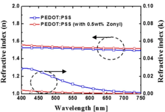
The complex refractive index of PEDOT:PSS was measured by a spectroscopic ellipsometer (M2000D) and Fig. 1 shows the results. The polynomial refractive indices expression for ITO, Alq3, TiO2, and Al were found in the literature [26–28]. The refractive
Fig. 1. The refractive indexes of PEDOT:PSS and PEDOT:PSS with 0.5wt% Zonyl were measured by a spectroscopic ellipsometer (M2000D).
3. Results and discussion
3.1 Spin-coated titanium dioxide nanoparticles
Fig. 2. Scanning electron microscope (SEM) images: (a) cross-section view of the spin-coated TiO2 nanoparticles on indium tin oxide (ITO) anode, (b) surface view of the spin-coated TiO2 nanoparticles on ITO, (c) (left) surface view of the spin coated TiO2 nanoparticles covered by poly(3,4-ethylenedioxythiophene)-poly(styrenesulfonate) (PEDOT:PSS), (right) surface view of the spin-coated TiO2 nanoparticles under the PEDOT:PSS layer, (d) cross-section view of the OLED device with the TiO2 nanoparticles inside the device.
Figure 2(a) shows a cross-sectional view of the spin-coated titanium dioxide nanoparticles on the ITO anode. The size of the nanoparticles was slightly distributed, and the particles were coated in the form of a layer. The height of the spin coated nanoparticles was around 40 nm and the roughness was under 10 nm. An atomic force microscope (AFM) was used to
measure the roughness, which was obtained as a root mean square value. As Fig. 2(b) shows, the nanoparticles were spread evenly along the surface without agglomeration. When the
OLED device was fabricated with TiO2 nanoparticles,
poly(3,4-ethylenedioxythiophene)-poly(styrenesulfonate) (PEDOT:PSS) was coated on the nanoparticles for improved electrical performance and a clear pixel image, and experiment to confirm whether the nanoparticles
were swept by PEDOT:PSS was conducted. The PEDOT:PSS covered the TiO2 nanoparticles
using a spin-coating method and then air plasma removed the PEDOT:PSS from the nanoparticles. The images presented in Fig. 2(c) are the surface of the PEDOT:PSS on the nanoparticles (left) and the surface of the device taken the air plasma (right). The nanoparticles also could be observed in the SEM image of the completely fabricated OLED device (Fig. 2(d)). From measurements, it was verified that the nanoparticles were not swept by spin-coated PEDOT:PSS.
3.2 Measurement results of OLEDs
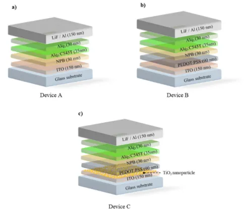
Fig. 3. The OLED device structures used in this study: (a) device A is a reference device that has Alq3:C545T as an emission layer, (b) device B contains a PEDOT:PSS layer on an ITO anode, (c) device C has spin-coated TiO2 nanoparticles between an ITO anode and PEDOT:PSS layer.
Figure 3 illustrates the structure of the OLED devices used in this study. Device A is a reference device that has tris(8-hydroxy-quinolinato) aluminum doped by 2,3,6,7-tetrahydro-1,1,7,7,-tetramethyl-1H,5H,11H-10-(2-benzothiazolyl) quinolizino-[9,9a,1gh] coumarin
(Alq3:C545T) as an emission layer, and device B contains a PEDOT:PSS layer on an ITO
anode. Device C has spin-coated TiO2 nanoparticles between an ITO anode and a
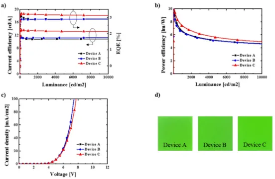
PEDOT:PSS layer. Figure 4(a) shows the current efficiency and EQE versus luminance. The
current efficiency of device C was 13.2cd/A and the EQE was 3.15% at 5000cd/m2
luminance. These results represent 23% and 9.7% increased values, respectively, compared
with device A, which had 10.7cd/A current efficiency and a 2.87% EQE at 5000cd/m2. The
respectively (Fig. 4(b)). The power efficiency of device C increased by 10.6% compared with the reference, device A. Figure 4(c) shows the electrical properties. Regardless of the structures, the currents were almost the same. As Fig. 4(d) shows, all of the pixels of devices A, B, and C were clear. The PEDOT:PSS surrounding the nanoparticles provided clear pixel images in device C because the spin coated PEDOT:PSS has 500 times higher conductivity in the parallel direction through the layer compared to the vertical direction [29]. The holes injected from the ITO and PEDOT:PSS might spread out through the spin coated PEDOT:PSS layer on the nanoparticles. The holes located throughout the PEDOT:PSS layer then result in a clear pixel image.
Fig. 4. The performance of the OLED devices: (a) current efficiency and EQE versus luminance, (b) power efficiency versus luminance, (c) current density versus voltage, (d) pixel images at 1.25mA/cm2.
3.3 Optical characteristics of OLEDs
The optical characteristics of the OLED device with TiO2 nanoparticles were calculated by a
microcavity simulation to analyze the optical characteristics of the fabricated OLED devices. The cavity enhancement factor, given by Eq. (1), is derived by multiplying two beam interference factor and a Fabry-Perot interference factor [30]. A schematic illustration of light interference inside the OLED device is shown in Fig. 5. Equation (2) represents the Fabry-Perot interference factor, which is also called multi-beam interference, and is defined as the interference of the group of reflected light from the cathode and the anode. I0 is the light
intensity, T is the transmittance of the anode side, and R denotes k02d
cathode anode
r ⋅r ⋅e−κ ,
where rcathode and ranode are absolute values of the cathode and anode side reflectance, respectively. κ is an imaginary part of the organic layer and d is the distance between the two interfaces at the anode and cathode side. φ denotes −φcathode−φanode+nk d02 , where
cathode
φ and φanode are the reflectance phase at the cathode and anode side, respectively [31]. Equation (3) is the equation for the two beam interference indicating the interference between the light emerging from the emission zone and the reflected light at the metal cathode. d is
the distance between the emission zone and the Al cathode.φ is −φcathode+nk d02 [31]. The calculated data of the transmittance and the reflectance at both the anode and cathode side were acquired from the characteristic matrix method [32].
Fig. 5. Schematic illustration of microcavity effect in an OLED device incorporating spin-coated TiO2 nanoparticles.
( ) ( ) ( ; ) cav FP TI G λ = f λ ×f λ d (1) 0 2 2 ( ) (1 ) 4 (sin ) 2 FP I T f R R λ = ⋅ φ − + (2) 02 2 02 0 ( ; ) [1 ( k d) 2 k d cos ] TI Al Al f λ d = ⋅ +I r ⋅e−κ + ⋅r ⋅e−κ ⋅ φ (3)
In order to calculate the transmittance and reflectance, the effective refractive index was applied to a layer composed of spin-coated TiO2 nanoparticles and PEDOT:PSS, which filled
the void area between the particles. The 0.8wt% TiO2 nanoparticle layer has less void area
compared with the 0.2wt% and 0.4wt% cases. However, the height of the TiO2 nanoparticle
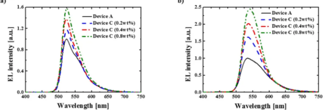
layer is the same regardless of the densities. The effective refractive index was determined by the ratio of nanoparticles and PEDOT:PSS. The electroluminescence (EL) spectra of OLED devices having different TiO2 nanoparticle densities were measured for comparison with the
simulation data (Fig. 6). Similar tendencies of the EL spectra were observed from the simulation and experimental data.
Fig. 6. EL spectra with different density of TiO2 nanoparticles: (a) experimental data, (b) simulation data
The simulation and experimental data from different total heights of TiO2 nanoparticles
and the PEDOT:PSS layer are presented in Fig. 7. Figures 7(a) and 7(b) plot the EL enhancement ratio of device C relevant to device A from the simulation and experiments, respectively. In Fig. 7(a), the peak of the EL enhancement ratios was red-shifted and decreased as the total height of the layer increased. A similar tendency of the changes in the EL enhancement ratio was found in the experimental device. The results of the microcavity simulation and the experimental data indicate that the microcavity was the main effect
manifested by the TiO2 nanoparticles inside the OLED device. Figure 7(c) shows SEM
images of cross section view of TiO2 nanoparticles and PEDOT:PSS total layer. In all cases
shown in Fig. 7(c) the roughness of the PEDOT:PSS on the TiO2 nanoparticle layer is sub 4.5
nm, which is almost flat. An AFM was used to measure the roughness, which was obtained as a root mean square value.
Fig. 7. Data from different total height of the TiO2 nanoparticles and PEDOT:PSS layer (70 nm, 90 nm, 110 nm, 130 nm): (a) simulation data of the EL enhancement ratio, (b) experimental data of the EL enhancement ratio, (c) cross-section view of TiO2 nanoparticles and PEDOT:PSS total layer from SEM image.
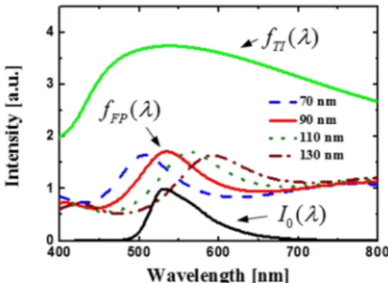
Fig. 8. Simulation results of the two-beam interference factor ( fTI( )λ ), Fabry-Perot interference factor ( fFP( )λ ) and active layer photo luminance intensity (I0( )λ ).fFP( )λ was simulated at four different total height (70 nm, 90 nm, 110 nm, 130 nm) of the TiO2 nanoparticle layer and PEDOT:PSS layer.
When the height of the nanoparticles and PEDOT:PSS was 90 nm, the resonance wavelength matched the device emission wavelength, which was the peak emission
wavelength of Alq3:C545T (Fig. 8). Furthermore, the EL enhancement ratio was high
compared with the other height of nanoparticles and PEDOT:PSS layer (Fig. 7). Therefore, the total height of the layer including the TiO2 nanoparticles and PEDOT:PSS was determined
as 90 nm for device C. Even though device B had a 90 nm height PEDOT:PSS layer, the performance of this device was similar to that of device A (Figs. 4(a), 4(b)). This supports that the TiO2 nanoparticles are responsible for the microcavity effect inside the device.
Fig. 9. (a) The normal direction transmittance (red circle), scattering transmittance (blue triangle), and reflectance (blue open triangle) of the layer composed of TiO2 nanoparticles and PEDOT:PSS having 90 nm thickness designed for the microcavity effect in the OLED with an Alq3:C545T emission layer. (b) Simulated reflectance data of the composed layer of the TiO2 nanoparticles covered by PEDOT:PSS having 90 nm for the microcavity effect in the OLED with an Alq3:C545T emission layer. The two different incident materials are NPB (black square) and air (red circle).
To confim the optical characteristics of the layer composed of TiO2 nanoparticles and
PEDOT:PSS, the transmittance and reflectance of the layer having 90 nm height were
measured. Even though the TiO2 nanoparticles were used in the OLED device, the normal
direction transmittance and the scattering transmittance had a difference of less than 5% (Fig. 9(a)). This result shows that the scattering effect by the nanoparticles is not the main reason for the enhanced device performance in the experiments. The slight changes between the normal direction and scattering transmittance might due to sub-10 nm surface roughness of the TiO2 nanoparticle layer [33].
Increased reflectance was observed adjacent to the green wavelength region. The increased reflection occured from the high refractive index of the TiO2 nanoparticles in
tandem with the optimized total height of the TiO2 nanoparticle and PEDOT:PSS layer [32].
The height of the layer dictated the peak reflection wavelength adjacent to the green wavelength using light interference [32]. Although the peak reflection wavelength should be 525 nm, which is the peak emission wavelength of Alq3:C545T, Fig. 9(a) shows that the peak
reflection wavelength shifted to the right side of 525 nm. This shift happened because air instead of NPB was the medium surrounding PEDOT:PSS when the measurement was conducted. As Fig. 9(b) shows, the reflection peak wavelength was adjacent to 525 nm when the surrounding medium was changed to N,N'-bis(naphthalen-1-yl)-N,N'-bis(phenyl)-benzidine (NPB), as in earlier OLED devices.
Fig. 10. Normalized luminous intensity of devices A, B, and C according to the viewing angle. The dashed line indicates lambertian light source.
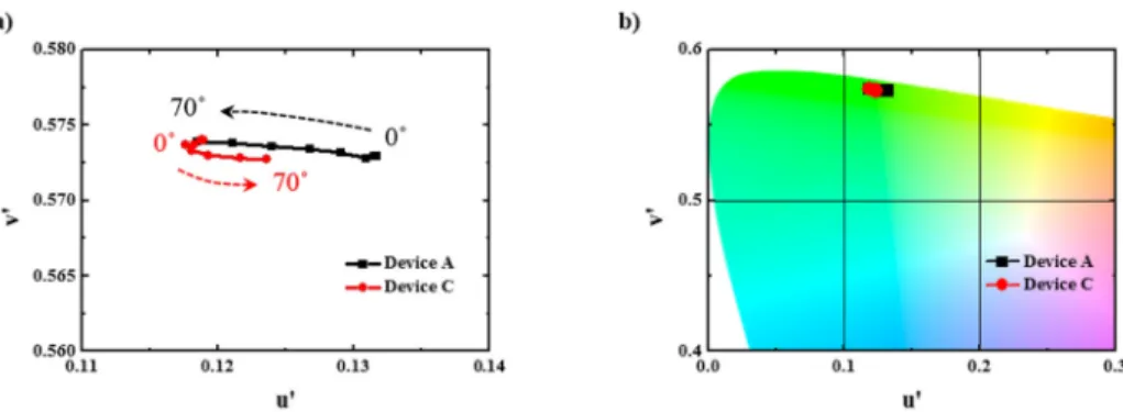
Fig. 11. (a) Changes of the color coordinates according to the viewing angle, (b) changes of the color coordinates depicted on the color space.
Figure 10 shows the normalized luminous intensity according to the viewing angle. The slight luminance angular dependency could be further evidence that the microcavity effect was the reason for the enhancement of the optical efficiency with TiO2 nanoparticles. Because
of the angular dependency, the EQE and the power efficiency of device C were improved by 9.7% and 10.6%, respectively, which provided less than 23% of the enhanced current efficiency. However, improvement of the optical efficiency still could be observed, and the change of the color coordinates according to the viewing angles was not severe, and thus device C is adequate for application to a display (Fig. 11).
3.4 Electrical characteristics of OLEDs
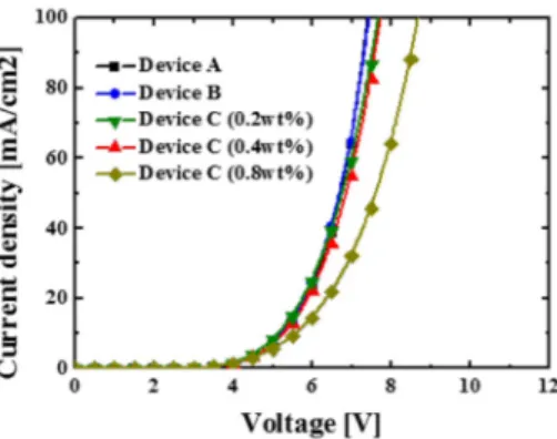
The electrical properties were fairly consistent among devices A, B, and C (Fig. 4(c)). The similar electrical characteristics might be caused by PEDOT:PSS filling the space between the TiO2 nanoparticles, because holes could be injected through the PEDOT:PSS rather than
TiO2 nanoparticles. Figure 12 shows that the OLED device with 0.8wt% TiO2
nanoparticleshad lower current density. There would be insufficient space between the 0.8wt% nanoparticles for the PEDOT:PSS, and the reduced amount of PEDOT:PSS would then result in fewer hole transporting paths. This indicates that the PEDOT:PSS in the space between nanoparticles assisted the holes to move toward the organic layers.
Fig. 12. Current density versus voltage graph of devices A, B, and C. Device C was divided into three groups by TiO2 nanoparticle density.
4. Conclusions
We have found that a microcavity effect realized by incorporating TiO2 nanoparticles can be
exploited to enhance the optical efficiency of OLEDs. A microcavity simulation and
experimental data confirmed that the microcavity was the main effect created by the TiO2
nanoparticles. The transmittance data show that scattering was not the main effect underlying the improved optical efficiency obtained in this study. The method suggested in this study is simple and cost effective, and also is suitable for mass production. Furthermore, the electrical properties and pixel image are not damaged by the proposed method. Becuase of the solution process, it affords a practical means of enhancing the optical property of polymer OLEDs.
Acknowledgments
This work was supported by the National Research Foundation of Korea(NRF) grant funded by the Korea government(MSIP)(CAFDC 5-1(0), NRF-2007-0056090)) and was also supported by the Global Leading Technology Program funded by the Ministry of Trade, Industry and Energy, Republic of Korea (10042477).