3-4 / J. H. Seo
• IMID 2009 DIGEST
Abstract
We demonstrated that the simple layered red phosphorescent organic light-emitting diodes are possible to have high efficiency and low driving voltage without hole injection and transport layers. The simplified OLED shows the max. current efficiency, power efficiency and quantum efficiency of 26.3 cd/A, 20.7 lm/W and 16.7 %, respectively.
1. Introduction
Since they first appeared in the 1980s, organic light-emitting diodes (OLEDs) have received much attention due to their potential use as a full-color display technology [1-6]. In general, the efficient OLEDs consist of hole injection layer (HIL), hole transporting layer (HTL), emission layer (EML), electron transporting layer (ETL) and electron injection layer (EIL) between anode and cathode. It has been already shown that performance improvement of OLED can be realized using a HIL/HTL structure due to a sequence of cascaded hole-injection barriers present in the HIL/HTL/EML structure [7-9]. However, this multi-layered structure of OLEDs rather increases the driving voltage and reduce the power efficiency of devices due to the increase of film thickness. In this paper, therefore, we demonstrate high efficiency red phosphorescent devices without using HIL/HTL layer.
2. Experimental
We fabricated the OLED devices with a structure of indium tin oxide (ITO) / 4,4′-N,N′-dicarbazole-biphenyl (CBP) doped with bis(2-phenylquinoline)
iridium(III)(acetylacetonate) [Ir(pq)2(acac)] (60 nm) /
4,7-diphenyl-1,10-phenanthroline (BPhen) (30 nm) / lithium quinolate (Liq) (2 nm) / aluminum (Al) (100 nm), where the doping concentration of red dopant,
Ir(pq)2(acac), was varied from 4 % to 20 %. The CBP
doped with Ir(pq)2(acac) and BPhen layers were used
as EML and ETL, respectively, without HTL.. The devices consist of the bilayer between the anode and cathode as ITO and Liq/Al, respectively. The device configuration was shown in Fig.1.
Fig.1. Device Configuration fabricated in this study.
The ITO coated glass was cleaned in an ultrasonic bath by following sequence: in acetone, methanol, diluted water and isopropyl alcohol. Thereafter,
pre-cleaned ITO was treated by O2 plasma with the power
conditions of 125 W for 2 min under low vacuum of 2
ⅹ 10-2 torr. All devices were fabricated in the high
vacuum (5 x 10⁻⁷ torr) and organic materials were
deposited by thermal evaporation of onto the surface of the ITO-coated glass substrate (30 Ω/sq, emitting area was 3 mm x 3 mm). The deposition rate was 1.0–
1.1 Å/sec for organic materials and 0.1 Å/sec for
Liq, respectively. After the deposition of the organic
A Simple Structural Red Phosphorescent Organic Light-Emitting diodes with high-efficiency and low-voltage
Ji Hyun Seo1, You Young Jin1, Hoe Min Kim1, Eun Young Choi1, Jun Ho Kim1, Kum Hee Lee2, Seung Soo Yoon2 and Young Kwan Kim1
1Dept. of Inform. Display, Hongik University, Seoul 121-791, Korea
Tel.:82-2-320-1646, E-mail:[email protected]
2Dept. of Chemistry, Sungkyunkwan University, Suwon 440-746, Korea
3-4 / J. H. Seo
IMID 2009 DIGEST •
layers without a vacuum break, the Al cathode was
deposited at a rate of 10 Å/sec. With the DC voltage
bias, the optical and electrical properties of the devices such as the current density, luminance, luminous efficiency, CIE coordinates and electroluminescence (EL) spectra characteristics were measured with Keithley 237 and CHROMA METER CS-1000 instruments, respectively. All measurements were carried out under ambient conditions at room temperature.
3. Results and discussion
We fabricated five devices without HTL that 4 %,
8 %, 12 %, 16 % and 20 % Ir(pq)2(acac) was doped in
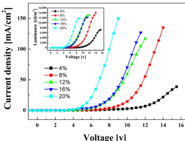
CBP. We found that the current density increases and the driving voltage reduces as the doping concentration increases as shown in Fig.2 and the inset of Fig.2, respectively. It means that the direct hole injection from ITO into dopant becomes dominant rather than hole injection to host followed by energy transfer from host to dopant as the doping concentration increases. It is because that the work function of pre-treated ITO (~ 5.0 eV) is nearly aligned with the highest occupied molecular orbital
(HOMO) level of Ir(pq)2(acac) (~ 5.2 eV). Therefore,
we can prove that HIL and HTL is actually unnecessary for the red OLED with similar energy level between the work function of anode and HOMO EML.
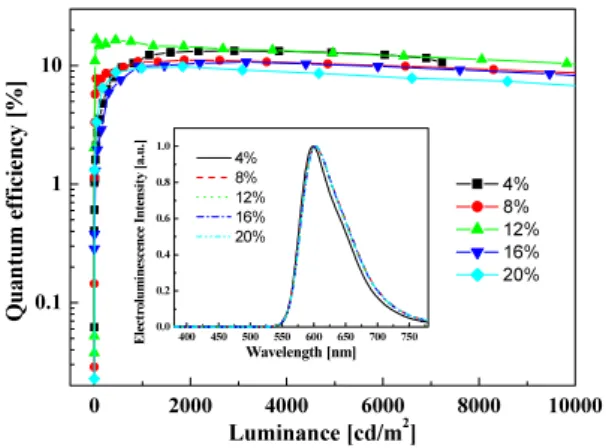
Figure 3 shows the luminance curves as current density increases. The current density and luminance are steadily increased as doping concentration increases in voltage standard graph, whereas the luminance at the doping concentration of more than 12 % was rather decreased in current density standard graph. That seems to be due to triplet-triplet annihilation of phosphorescent emitter with long decay-lifetime. This tendency was also similarly observed in the efficiency vs current density graphs. Figure 4, inset of Fig.4 and Fig.5 show the luminous efficiency, power efficiency and quantum efficiency of devices without HIL/HTL, respectively. The best efficiencies were obtained in device with 12 % doping ratio, and the efficiencies were rather decreased at more than 12 % doping ratio. The luminous efficiencies of devices with doping concentrations of 4 %, 8 %, 12 %, 16 % and 20 % are 23.5 cd/A, 17.9 cd/A, 26.3 cd/A, 16.6 cd/A and 15.3 cd/A, respectively. The power efficiencies of devices with doping concentrations of 4 %, 8 %, 12 %, 16 % and 20 % are 6.0 lm/W, 6.5 lm/W, 20.7 0 2 4 6 8 10 12 14 16 0 50 100 150 0 2 4 6 8 10 12 14 16 0 2,000 4,000 6,000 8,000 10,000 12,000 14,000 16,000 4% 8% 12% 16% 20% Lu mi na nc e [ cd /m 2] Voltage [v] 4% 8% 12% 16% 20% Cu rre nt de ns ity [m A/ cm 2] Voltage [v]
Fig.2. Current density (inset; luminance) vs voltage curves of simplified OLEDs with various doping concentration. 0 20 40 60 80 100 120 140 160 0 2,000 4,000 6,000 8,000 10,000 12,000 14,000 16,000 4% 8% 12% 16% 20% Lu mi na nc e [ cd /m 2]
Current density [mA/cm2]
Fig.3. Luminance vs current density curves of simplified OLEDs with various doping concentration. 0 2000 4000 6000 8000 10000 0.1 1 10 0 2000 4000 6000 8000 10000 0.1 1 10 4% 8% 12% 16% 20% Po we r e ffic ien cy [lm /W ] Luminance [cd/m2] 4% 8% 12% 16% 20% Lu mi no us ef fic ien cy [c d/A ] Luminance [cd/m2]
Fig.4. Luminous efficiency (inset; power efficiency) vs luminance curves of simplified OLEDs with various doping concentration.
3-4 / J. H. Seo • IMID 2009 DIGEST 0 2000 4000 6000 8000 10000 0.1 1 10 400 450 500 550 600 650 700 750 0.0 0.2 0.4 0.6 0.8 1.0 4% 8% 12% 16% 20% Ele ctr olu mi ne sce nc e I nte nsi ty [a. u.] Wavelength [nm] 4% 8% 12% 16% 20% Qu an tum ef fic ien cy [% ] Luminance [cd/m2]
Fig. 5. Luminous efficiency (inset; power efficiency) vs luminance curves of simplified OLEDs with various doping concentration.
lm/W, 7.3 lm/W and 9.6 lm/W, respectively. Moreover, the quantum efficiencies of 13.4 %, 11.2 %, 16.7 %, 10.8 % and 9.8 % were observed in devices with doping concentrations of 4 %, 8 %, 12 %, 16 % and 20 %, respectively. It was also found that all devices have the stable electrical characteristics with low roll-off in efficiency. For the device with doping concentration of 12 %, the external quantum efficiency at a luminance of 10,000
cd/m2 was maintained at about 62.9 %, which is
10.5 % of its maximum external quantum efficiency having 16.7 %. On the other hands, the electroluminescence (EL) spectra of devices with various doping concentrations show the same
emission peak at about 600 nm due to Ir(pq)2(acac),
as shown in inset of Fig. 5.
4. Summary
In OLEDs, HIL and HTL are traditionally are required for the efficient injection and transport of hole into the EML. However, we developed that the simplified red phosphorescent OLEDs lead to the high efficiency and low driving voltage without HIL and HTL layer. It is also possible by the direct hole injection from anode into dopant of EML. These simplified OLEDs have the advantage of low cost manufacturing and can be applied for the full-color OLED display and also lighting.
Acknowledgement
This work was supported by Energy Resources
Technology Development program (2007-E-CM11-P-07) and Strategy Technology Development program (10030834) from Ministry of Knowledge Economy (MKE).
5. References
1. C. W. Tang, S. A. Vanslyke, Appl. Phys. Lett., 51,
p.913 (1987).
2. D. S. Qin, Y. Tao, J. Appl. Phys., 97, p.044505
(2005).
3. C. W. Tang, Appl. Phys. Lett., 48, p.183 (1986).
4. G. Yu, Y. Cao, J. Wang, J. McElvain, A. J. Heeger,
Synth. Met., 102, p.904 (1999).
5. P. Peumans, V. Bulovic, S. R. Forrest, Appl. Phys.
Lett., 76, p.3855 (2000).
6. L. P. Ma, J. Liu, Y. Yang, Appl. Phys. Lett., 80,
p.2997 (2002).
7. Z. B. Deng, X. M. Ding, S. T. Lee, W. A. Gambling,
Appl. Phys. Lett., 74, p.2227 (1999).
8. H. Jiang, Y. Zhou, B. S. Ooi, Y. Chen, T. Wee, Y. L.
Lam, J. Huang, S. Liu, Thin Solid Films, 363, p.25
(2000).
9. S. F. Chen, C. W. Wang, Appl. Phys. Lett., 85, p.765