Soft-Switching Auxiliary Current Control for Improving Load Transient
Response of Buck Converter
Doogwook Kim, Joonho Shin, and Jong-Won Shin
School of Energy Systems Engineering, Chung-Ang UniversityABSTRACT
A control technique for the auxiliary buck/boost converter is proposed herein to improve the load transient response of the buck converter. The proposed technique improves the system efficiency by enabling the soft switching operation of the auxiliary converter. The design guidelines for achieving capacitor charge balance for the output capacitor during the transient are also presented herein. The experimental results revealed that the output voltage undershoot and settling time during the load step-up transient were 40 mV and 14 μs, respectively, and the output voltage overshoot and settling time during the load step-down transient were 35 mV and 21 μs, respectively. The performance and effectiveness of the proposed technique were experimentally verified using a prototype buck converter with a 15-V input, 3.3-V output, and 200-kHz switching frequency.
1. Introduction
Various control techniques have previously been developed to improve the load transient response of the buck converter. The time-optimal control based on the capacitor charge balance (CCB) enables minimum output voltage fluctuation without the aid of auxiliary circuits[1].
Previous studies have emphasized the simple implementation and operation of resistive auxiliary circuits[2]-[3]. The auxiliary switched resistor attenuates
the output voltage fluctuation, reduce the efficiency, and increase the electromagnetic interference (EMI) caused by the high di/dt of the switches[2]. The auxiliary inductor and bidirectional switches require complicated control circuits and impose a heavy computational burden on the digital integrated circuit (IC)[3]. Additionally, the resistance in the
freewheeling path degrades the efficiency.
Control techniques employing nonresistive auxiliary circuits can also improve the dynamic response[4]-[6]. The
auxiliary inductor exploits the resonance and soft switching[4], but the auxiliary switches must be controlled
differently and according to whether the load is stepped up or down, which increases the controller complexity. The high-frequency switching controllers of the auxiliary circuit have been described in previous papers[5]-[6]. The
average current of the auxiliary inductor has been controlled to a constant value to achieve CCB during the load transient[5]. Adaptive slope control has also been
proposed to further improve the load transient response[6].
However, these control techniques require high-bandwidth sensors and high-speed digital ICs, which increase the controller complexity.
This paper proposed a technique for peak-current-controlling the auxiliary current in critical conduction mode (CRM). The technique minimizes the output voltage deviation during the load transient through cycle-by-cycle CCM, while the soft turn-on of the auxiliary switches suppresses the efficiency degradation and EMI generation. The remainder of this paper is organized as follows; Section 2 describes the circuit operation and design conducted via the proposed control scheme. The experimental results are presented in Section 3, and the conclusions are presented in Section 4.
2. Proposed Control Technique
2.1 Implementation of proposed control circuit Fig. 1 shows the main converter (Q1, Q2, and L1) and
auxiliary buck/boost converter (Q3, Q4, and L2) connected
in parallel. The literals Vin, vO, iL1, iL2, and iO denote the
input voltage, output voltage, main inductor current, auxiliary inductor current, and load current, respectively. The voltages vgsi and vdsi denote the gate-source and
drain-source voltages of the metal-oxide-semiconductor field-effect transistor (MOSFET) Qi, respectively. In the
steady state, Q3 and Q4 are turned off, while Q1 and Q2 are
operational via the conventional voltage mode controller (VMC). During the load transient, Q3 and Q4 operate along
with Q1 and Q2 to control iL2 and improve the transient
response.
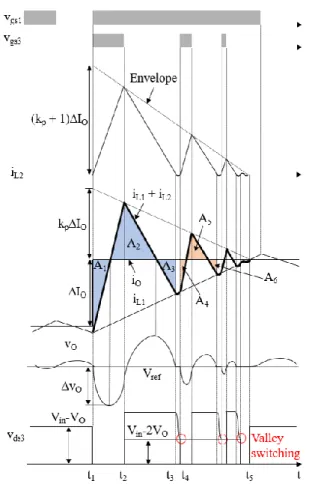
The key waveform of the proposed auxiliary current control is shown in Fig. 2. The literals Vref and ∆IO are the
target output voltage and magnitude of the iO variation,
respectively. During the transient period caused by stepping up iO and t1-t5, Q1 is fully turned on while Q2 is
Fig. 1. Main buck converter (Q1, Q2, and L1) and auxiliary
buck/boost converter (Q3, Q4, and L2) for applying proposed
auxiliary current control.
160
fully turned off shown in Fig. 2. The auxiliary converter works as a peak-current-mode-controlled buck converter in the CRM. Switch Q3 operates as the main switch of the
auxiliary buck converter to produce the triangular wave shapes of iL2 under an envelope. The first switching period
of the auxiliary converter comprises three switching states: ⚫ State 1 [t1-t2]: Current iO is stepped up at t1; Q3 turns
on, and iL2 increases linearly.
⚫ State 2 [t2-t3]: When iL2 reaches the envelope at t2,
Q3 turns off, and iL2 decreases and freewheels through
the body diode of Q4. Switch Q4 can be ON as a
synchronous rectifier to reduce the conduction loss. ⚫ State 3 [t3-t4]: When iL2 reaches zero at t3, the output
parasitic capacitances of Q3 and Q4 and L2 resonate.
Switch Q3 turns on again at t4, when vds3 is minimum.
During this state, the vO variation is assumed to be
negligible.
These states are repeated N times before the steady-state operation resumes and VMC regains control at t5. The
number N can be limited to avoid the risk of excessively high switching frequencies and power losses. The switching loss of Q3 is minimized via valley switching, that
is, by Q3 turning on at the valley of vds3. Switch Q3 may turn
on with zero-voltage switching (ZVS) if Vin2vO.
Area An represents the amount of charge that is charged
to or discharged from the output capacitor CO, to which the
vO deviation is proportional. The coefficient kp is set to
maintain the CCB of CO in each switching cycle, as
expressed in (1).
(
)
2 1 1,4,7,
i i i
A+A+ =A+ i= (1)
Section 2.2 presents the derivation of kp in detail. The
undershoot of vO, ΔvO, is the function of voltages,
inductances, and ΔIO and is solely determined by A1, as
expressed in (2).
(
)(
)
2 1 2 1 21
2
O o in O O COA
I L L
v
C
=L L
V
V
=
+
−
(2)When iO is stepped down, the auxiliary converter
operates as a peak-current-mode-controlled boost converter in CRM. Switch Q4 acts as the main switch of the
auxiliary boost converter and turns on with ZVS if Vin2vO, while Q1 is fully off and Q2 is fully on.
2.2 Envelope for Capacitor-Charge-Balance The magnitude of iL2 is controlled by the envelope of
which height is (kp+1)ΔIO as shown in Fig. 2. The constant
kp is a function of Vin, VO, L1, and L2 and is independent
from ΔIO, as expressed in (3).
(
)
(
)
1 2 1 2 2 2 O in O p O in O LV L V V k LV L V V − − = + − (3)The other constant kn that determines the envelope when iO
is stepped down can be obtained using (4).
(
)
(
)
(
)
(
)
1 2 1 2 2 2 in O in O n in O in O L V V L V V k L V V L V V − + − − − = − (4)In practical implementation, the first turn-on of Q3 may
be delayed by the time ∆td from the step change of iO. Fig.
3 plots kp and kn versus vO when Vin, L1, L2, and IO are as
presented in Table 1. The plots are symmetric with respect
Fig. 2. Key waveforms of proposed auxiliary current control when iO is stepped up (N=3).
Fig. 3. kp (solid curves) and kn (dotted curves) versus vO
under conditions defined in Table 1. Table 1. Circuit parameters of experiment.
Parameter Description
Vin 15 V
vO 3.3 V
iO 4 A-15 A
Switching frequency of Q1 and Q2 200 kHz
L1 10 uH
L2 500 nH
CO 220 uF
-to the VO = Vin/2 line (7.5 V in this paper) when ∆td=0,
because the increasing and decreasing slope of iL1+iL2 are
interchanged between the step-up and step-down cases of iO. The nonzero ∆td increases both kp and kn.
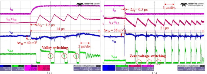
3. Experimental Verification
The prototype circuit shown in Fig. 1 was built; its parameters are listed in Table 1. The VMC control loop had a 78.6° phase margin at the 12-kHz cutoff frequency via a PIC type-3 compensator and the control circuit was configured by analog ICs only. Fig. 4 shows the experimental waveform of iO (magenta trace), iL1+iL2 (red),
vO (blue), vds3 and vds4 (green) of the proposed control
scheme when iO was stepped up and down, respectively.
The delay ∆td was 1.2 μs at up and 0.5 μs at
step-down. In Fig. 4(a), The measured undershoot voltage and settling time were 40 mV and 14 μs, respectively. As can be seen, Q3 valley-switched to reduce the switching loss
and noise. In Fig. 4(b), the measured overshoot voltage and settling time were 35 mV and 21 μs, respectively. The Q4
was zero-voltage-switched, reducing switching loss and noise during the load step-down transient.
4. Conclusion
An auxiliary current control technique is proposed herein to improve the load transient response of buck converter. The proposed scheme controls the auxiliary buck/boost converter through the peak current mode in CRM. The proposed control scheme minimizes the output voltage deviation and power loss of the auxiliary circuit via soft-switching auxiliary switches. Experimental results by 15 V-3.3 V, 200-kHz buck converter demonstrated the improved dynamic response: the undershoot was 40 mV and the settling time was 14 μs when the output current was stepped from 4 A to 15 A, and the overshoot was 35
mV and settling time was 21 μs when the output current was stepped from 15 A to 4 A.
References
[1] E. Meyer, Z. Zhang, and Y. F. Liu, “An optimal control method for buck converters using a practical capacitor charge balance technique,” IEEE Trans. Power Electron., vol. 23, no. 4, pp. 1802-1812, Jul. 2008. [2] S. Kapat, P. S. Shenoy, and P. T. Krein, “Near-null
response to large-signal transients in an augmented buck converter: a geometric approach,” IEEE Trans. Power Electron., vol. 27, no. 7, pp. 3319-3329, Jul. 2012.
[3] W. Lu, Z. Zhao, Y. Ruan, S. Li, and H. H. C. Iu, “Two-period frame transient switching control for buck converter using coupled-inductor auxiliary circuit,” IEEE Trans. Ind. Electron., vol. 66, no. 10, pp. 8040-8050, Oct. 2019.
[4] Z. Shan, S. C. Tan, C. K. Tse, and J. Jatskevich, “Augmented buck converter design using resonant circuits for fast transient recovery,” IEEE Trans. Power Electron., vol. 31, no. 8, pp. 5666-5679, Aug. 2016.
[5] E. Meyer, Z. Zhang, and Y. F. Liu, “Controlled auxiliary circuit to improve the unloading transient response of buck converters,” IEEE Trans. Power Electron., vol. 25, no. 4, pp. 806-819, Apr. 2010. [6] Y. Wen and O. Trescases, “DC-DC converter with
digital adaptive slope control in auxiliary phase for optimal transient response and improved efficiency,” IEEE Trans. Power Electron., vol. 27, no. 7, pp. 3396-3409, Jul. 2012.
This research was supported by Energy Cloud R&D Program through the National Research Foundation of Korea(NRF) funded by the Ministry of Science, ICT (2019M3F2A1073313).
(a) (b)
Fig. 4. Experimental waveforms of proposed control technique; trace iO (magenta) is in 10 A/div; trace iL1 + iL2 (red) is in 20 A/div;
trace vO (blue) is in 100 mV/div. with AC coupling; trace vds3 or vds4 (green) are in 10 V/div. (a) When iO is stepped up from 4 to 15 A
with N = 4; time scale is 2 μs/div. (b) When iO is stepped down from 15 to 4 A with N = 10; time scale is 3 μs/div.