전해 도금을 이용한 높은 접착 특성을 갖는 섬유 기반 웨어러블 디바이스 제작
김형구1,3·노호균2·차안나1·이민정1·박준범3·정탁3·하준석1,2,†
1전남대학교 신화학소재공학과
2전남대학교 CORE 에너지 융복합 전문 핵심연구지원센터 3한국광기술원 차세대 LED 연구센터
Fabrication of Fabric-based Wearable Devices with
High Adhesion Properties using Electroplating Process
Hyung Gu Kim1,3, Ho Kyun Rho2, Anna Cha1, Min Jung Lee1, Jun-beom Park3, Tak Jeong3, and Jun-Seok Ha1,2,†
1Department of Chemicals Engineering, Chonnam National University, 77 Yongbong-ro, Buk-gu, Gwangju 61186, Korea 2Energy Convergence Core Facility, Chonnam National University, 77 Yongbong-ro, Buk-gu, Gwangju 61186, Korea
3Next generation LED research Center, Korea Photonics Technology Institute, Buk-gu, Gwangju 61007, Korea (Received March 15, 2021: Corrected March 27, 2021: Accepted March 30, 2021)
초 록: 유연한 특성을 유지하면서 높은 접착력을 가진 웨어러블 디스플레이를 제작하기 위하여 전해도금법을 이용한 접착법을 진행하였다. 또한 섬유에 접착된 LED의 사파이어 기판을 제거하기 위하여 LLO 전사법을 이용하였다. 그 후 전해도금을 이용한 접착법을 진행한 샘플의 SEM, EDS 데이터를 통하여 실제로 구리가 섬유직물의 격자사이를 관통하 여 성장하며 광원과 섬유를 고정시켜주는 것을 확인하였다. 구리의 접착특성을 확인하기 위하여 Universal testing machine (UTM)을 이용하여 측정하였다. 도금 접착 후 laser lift-off (LLO) 전사공정을 완료한 샘플과 전사공정을 진행하 지 않은 LED의 특성을 probe station을 이용하여 비교하였다. 공정 이후의 광원의 특성을 확인하기 위하여 인가 전류에 따른 electroluminescence (EL)을 측정하였다. 전류가 증가할수록 온도가 상승하여 Bandgap이 감소하기 때문에 spectrum 이 천이하는 것을 확인하였다. 또한 radius 변화에 따른 샘플의 전기적 특성 변화를 probe station을 이용하여 확인하였다. Radius 변형에도 구리가 bending stress를 견딜 수 있는 기계적 강도를 가지고 있어 Vf변화는 6% 이하로 측정되었다. 이 러한 결과를 토대로 웨어러블 디스플레이 뿐만 아니라 유연성이 필요한 배터리, 촉매, 태양전지 등에 적용되어 웨어러블 디바이스의 발전에 기여할 수 있을 것으로 기대한다.
Abstract: In order to produce wearable displays with high adhesion while maintaining flexible characteristics, the adhesive method using electro plating method was carried out. Laser lift-off (LLO) transcription was also used to remove sapphire substrates from LEDs bonded to fibers. Afterwards, the SEM and EDS data of the sample, which conducted the adhesion method using electro plating, confirmed that copper actually grows through the lattice of the fiber fabric to secure the light source and fiber. The adhesion characteristics of copper were checked using Universal testing machine (UTM). After plating adhesion, the characteristics of the LLO transcription process completed and the LED without the transcription process were compared using probe station. The electroluminescence (EL) according to the enhanced current was measured to check the characteristics of the light source after the process. As the current increases, the temperature rises and the bandgap decreases, so it was confirmed that the spectrum shifted. In addition, the change in the electrical characteristics of the samples according to the radius change is confirmed using probe station. The radius strain also had mechanical strength that copper could withstand bending stress, so the Vf variation was measured below 6%. Based on these results, it is expected that it will be applied to batteries, catalysts, and solar cells that require flexibility as well as wearable displays, contributing to the development of wearable devices.
Keywords: LED, Fabric, Electro plating, Laser lift off, Wearable display, Plating adhesion
†Corresponding author
E-mail: [email protected]
© 2021, The Korean Microelectronics and Packaging Society
This is an Open-Access article distributed under the terms of the Creative Commons Attribution Non-Commercial License(http://creativecommons.org/ licenses/by-nc/3.0) which permits unrestricted non-commercial use, distribution, and reproduction in any medium, provided the original work is properly cited.
우 높은 유연성을 가지고 있고, 실제 의류에 사용되는 소 재이기 때문에 실생활에 웨어러블 디바이스를 적용하기 위한 소재로 많이 활용되고 있다.16-19) 그러나 직물과 같
은 플렉시블한 기판의 경우 섬유의 직물 구조 때문에 fabric display를 제작하는데 큰 어려움이 있다.20) 이를 해
결하기 위한 Flexible fiber display에 대한 연구가 많이 보 고되었다.21)그러나 직접 wire에 ZnO, polymer, CNT sheet
를 붙이는 복잡한 제조 공정을 거쳐야하기 때문에 높은 비용과 낮은 생산성으로 인해 대량생산 제작에 어려움이 있다.22) 이러한 제조 공정의 단순화는 추후 대량생산과 다양한 분야에서의 적용을 위하여 개선이 필요한 부분이 다. 또한 섬유 기판을 활용한 디스플레이를 지속적으로 사용하기 위해서는 높은 유연성과 몸의 움직임에 의해 발 생하는 의류의 변형에 견딜 수 있어야한다. 그래서 의류 의 변형 및 지속적인 스트레스를 견딜 수 있는 섬유와 광 원 간의 높은 접착력이 필요하다. 특히 광원을 직접 섬유 에 접착하는 경우, 광원이 섬유의 유연성으로 인한 지속 적인 bending 스트레스에 의하여 광원의 contact 영역에 크랙(crack)을 유발하거나 끊길 수 있다.23) Crack의 발생
은 광원의 radiance 및 Current intensity, Vf 특성을 저하시
킬 수 있으며, 부분 발광의 원인이 될 수 있다. 이러한 문제를 해결하기 위하여 CNT, graphene oxide (GO)를 이용한 접착력 개선에 대한 결과도 있으나,24)이 에 대한 연구가 아직 많이 이루어지지 않아 유연성 기판 상 접착에 대한 연구가 필요하다. 본 연구에서는 전해도금 공정을 이용하여 섬유와 LED 를 접착하여 고접착 특성을 가진 웨어러블 디바이스를 제 작하였다. 전해 도금 공정으로 섬유에 접착된 LED의 표 면 및 도금된 금속의 성분을 확인하기 위하여 Scanning Electron microscope (SEM, Zeiss), Energy-dispersive X-ray spectroscopy (EDS, Zeiss)을 이용하였다. 또한 도금 접착 된 샘플의 접착력을 확인하기 위하여 Universal testing machine (UTM, Shimadzu)을 이용하였다. 도금 접착 후 전 사 공정 진행을 마친 샘플의 전기적 특성을 확인하기 위 하여 Probe station을 이용하여 Vf 와, electroluminescence
(EL)측정하였다.
2. 실
험
전체적인 공정은 Fig. 1과 같이 광원 제작 및 seed layer 증착, 섬유부착 후 구리 전해도금을 통한 섬유와 광원 접
다. 총 7 µm의 두께를 Inductively coupled plasma (ICP, Vacuum science)를 이용하여 BCl3/Cl2 가스로 etching하였
다. Mesa 공정 또한 동일한 방법으로 진행하여 2.5 µm etching하였다. LLO 전사 공정 진행 시 laser의 강한 출력 에 의한 광원의 피해를 최소화하기 위하여 n-GaN 영역에 UV-absorption layer로 Indium tin oxide (ITO)를 ITO E-beam을 이용하여 증착하였다. 이후 680oC의 조건으로 산 소 분위기에서 열처리를 진행하였다. 광원의 광 손실을 최소화하기 위하여 Ni/Ag/Ni/Au(550 nm) Reflector layer 를 E-beam을 이용하여 증착 하였다. 이후 reflector metal 의 adhesion을 향상시키기 위하여 430oC에서 Rapid
thermal annealing (RTA, Korea vacuum tech) 열처리를 진 행하였다. Passivation layer로 SiO2 (300 nm)을 Plasma
enhanced chemical vapor deposition (PECVD, OERLIKON) 를 이용하여 증착 하였다. 제작된 광원에 Polymer(NR) coating을 진행하였다. 이후 UV curing을 하고 170℃ 조 건에서 10분간 baking하였다. reflector 부분이 드러나도록 ICP를 이용하여 O2 plasma etching을 진행하였다. 그 후 전해도금의 seed layer를 증착 하기 위하여 E-beam을 이 용하여 Ti/Ni/Ti/Cu (1.2 µm)을 증착 하였다. 위 모든 과정 은 Energy Convergence Core Facility, Chonnam National University에 있는 Yellow room과 공정 room에서 진행하 였다. 2.2. 전해 도금을 이용한 광원과 섬유 접착 광원과 fabric을 최대한 밀착시키고 도금 틀을 이용하 여 LED와 fabric을 고정하였다. 고정된 샘플을 구리 전해 도금조에 넣어 전류를 3A 조건으로 인가하여 전해 도금 을 진행하였다. 샘플에 원활한 용액 공급을 위하여 도금 공정을 진행하면서 교반기를 이용하여 400 rpm 조건으 로 교반 하였다. 도금 시간은 총 3시간을 진행하였다. 2.3. LLO 전사기법을 이용한 광원과 사파이어 기판 분리 도금공정을 완료하여 접착이 된 LED와 LED기판을 분 리하기 위하여 LLO(Laser lift-off, QMC) 전사 공정을 진 행하였다. LED chip 면적과 chip 간 간격이 550 µm이다. laser beam의 크기가 550 µm 이상이 되면 chip에 laser 영 역이 중복되는 경우가 발생한다. 이는 chip의 crack을 야 기한다. 그렇기 때문에 Laser beam 면적은 550 × 550 µm2
로 설정하였다. Power는 42 W 조건으로 전사 공정을 진 행하였다.
2.4. 섬유에 접착이 된 광원의 특성 분석 및 비교
전해 도금 공정으로 섬유에 접착된 LED의 표면 및 도 금된 금속의 성분을 확인하기 위하여 SEM, EDS를 이용 하였다. 또한 도금 접착된 샘플의 접착력을 확인하기 위 하여 Universal testing machine (UTM, Shimadzu)을 이용 하였다. 도금 접착 후 전사 공정 진행을 마친 샘플의 전 기적 특성을 확인하기 위하여 Probe station을 이용하여 Vf, electroluminescence (EL) 측정하였다.
3. 결과 및 토론
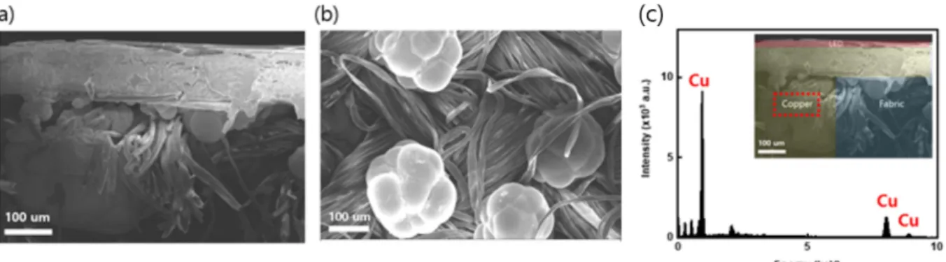
Fig. 2(a)~(c)는 전해도금 및 전사공정을 진행한 후 샘플 의 단면, 섬유 표면을 SEM 및 EDS로 확인한 이미지이다 . 그 중에서 Fig. 2(a)와 (b)를 통하여 전해도금 공정을 통 하여 섬유 직물의 격자 사이를 구리가 관통하는 형태로 성장하였음을 확인하였다. 전해도금의 특성상 전류가 흐 르는 부분에 구리가 도금된다. 때문에 구리가 섬유 사이 로 성장한 후 구리 이온을 공급 받을 수 있는 면적이 넓 어져[25]단추 형태로 성장하여 LED와 섬유를 고정하는 역할을 수행한다. Fig. 2(c)와 같이 성장된 물질을 EDS를 통하여 확인한 결과 실제로 섬유를 관통하여 성장한 물 질이 구리임을 확인하였다.Fig. 3(a)는 3시간 도금 접착 후 UTM을 이용하여 접착 력을 측정한 방법을 나타낸 이미지이다. 3시간 도금 후 UTM의 상단부에 기판을 고정하고 하단부에 섬유를 고 정하여 잡아당기는 방식으로 접착력을 측정하였다. Fig.
Fig. 3. (a) the method of measuring the adhesion of samples using UTM after the electroplating process, (b) the results of measuring the adhesion of samples
Fig. 2. (a) SEM cross section of samples with electroplating and laser lift off process, (b) copper grown through fiber SEM, (d) EDS results of material penetrating between fiber grids.
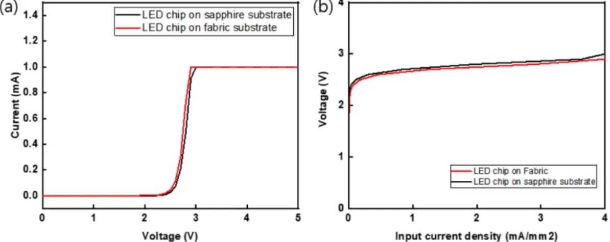
station을 이용하여 1 mA 기준으로 광원의 전기적 특성을 확인하였다. Fig. 4(a)는 광원의 전해도금 접착 전후의 I-V curve를 통한 순방향 turn-on voltage (I-Vf)값을 확인하였
고, 전해도금이 진행된 광원의 경우가 Vf 값이 더 작게 나 온 것을 확인할 수가 있다. Fig. 4(b)에서 또한 같은 Input current density 조건에서 더 낮은 전압 값이 측정되었다. 이는 NR 코팅이 passivation 역할을 하여 전류의 leakage 를 막아주었다.27) 또한 p-GaN에 구리 도금을 이용하여 접 착을 진행하였기 때문에 전도성이 증가하여 특성이 향상 되었다. Fig. 5(a)와 같이 전사공정 후 기판을 분리한 샘플의 광 특성을 확인하기 위하여 인가 전류에 따른 단일 Chip의 electroluminescence (EL) spectra 측정을 진행하였다. Fig.
섬유에 접착을 진행하였기 때문에 섬유의 유연함에 의 한 스트레스로 섬유에 접착된 광원이 탈락되어 연결이 이 루지지 않아 발광이 되지 않는 현상이 발생한다. 이러한 탈락 문제는 접착력이 높을수록 감소한다. 그래서 굽힘 정도에 따른 광원의 특성에 변화가 있는지 확인할 필요 가 있다. Fig. 6(a)는 굽힘 정도에 따른 발광하는 샘플의 이미지이다. 10 cm부터 1 cm까지 굽힘 정도를 달리하여 전기적 특성을 확인하였다. Fig. 6(b)는 bending stress에 의하여 전기적 특성을 확인하기 위하여 굽힘 정도를 다 르게 하였을 때의 Vf와 radius에 변화를 주지 않은 값을
비교하였다. 또한 이에 radius에 변형을 주지 않은 샘플을 기준으로 하여 변화율을 측정하였다. 그 결과 radius에 변 화를 주지 않은 LED의 Vf는 1 Ma 기준 2.9 V가 측정되
Fig. 5. (a) luminescent images, (b) electroluminescence (EL) spectra of samples manufactured through adhesive and transcription processes. Fig. 4. (a) I-V curve, (b) Voltage-Input current durability of LEDs that have completed all processes and LEDs before the adhesive and
었고 radius를 변형하더라도 변화를 주지 않은 LED와 6% 이내의 변화율의 가진 전기적 특성을 보였다. 이는 광원 과 섬유 사이에 도금된 구리가 변화한 radius에 의한 bend stress를 견딜 수 있는 기계적 강도와 섬유와 광원을 고정 하는 접착력을 가지고 있음을 의미한다.29)
4. 결
론
고 접착력을 가진 웨어러블 디스플레이를 제작하기 위 하여 전해도금법을 이용한 접착법을 진행하였다. 또한 섬 유에 접착된 LED의 사파이어 기판을 제거하기 위하여 LLO 전사법을 이용하였다. 그 후 전해도금을 이용한 접 착법을 진행한 샘플의 SEM, EDS 데이터를 통하여 실제 로 구리가 섬유직물의 격자사이를 관통하여 성장하여 광 원과 섬유를 고정시켜주는 것을 확인하였다. 접착특성을 확인하기 위하여 UTM을 이용하여 측정한 결과, 1506 gf/ 25mm가 측정되었다. 전해도금 접착 후 LLO 전사공정을 완료한 샘플과 어떠한 공정도 진행하지 않은 LED의 특 성을 probe station을 이용하여 비교하였다. 모든 공정을 진행한 샘플이 Vf 특성이 더 좋게 나왔는데 이는 NR coating이 passivation의 역할을 수행하였기 때문이다. 모 든 공정을 완료한 샘플의 인가 전류에 따른 EL을 측정하 였을 때 전류가 증가할수록 온도가 상승하여 감소한 bandgap에 의하여 spectrum이 적색 천이하는 것을 또한 확인하였다. 또한 radius 변화에 따른 샘플의 전기적 특성 변화를 probe station을 이용하여 확인하였다. Radius 변형 에도 구리가 bending stress를 견딜 수 있는 기계적 강도 를 가지고 있어 Vf 변화는 6% 이하로 측정되었다. 이러한 결과를 바탕으로 LED 이외의 bio sensors, battery 등 다양한 분야에 적용 가능할 것으로 기대한다.
감사의 글
이 논문은 교육과학기술부의 재원으로 한국연구재단의 이공분야 기초연구사업 (2018R1D1A1B07051009)과 교육 부의 재원으로 한국 기초과학지원연구원 국가연구시설 장 비 진흥센터의 지원을 받은 기초과학 연구역량강화사업 핵심연구지원센터 조성지원 과제에서 에너지 융복합 전 문핵심 연구지원센터를 조성하여(2019R1A6C1010024) 수 행된 연구임.참고문헌
1. Pan, S., Yang, Z., Chen, P., Deng, J., Li, H., & Peng, H, “Wearable Solar Cells by Stacking Textile Electrodes”, Ang-ewandte Chemie, 126(24), 6224-6228 (2014).
2. Corbishley, P., & Rodriguez-Villegas, E, “Breathing Detection: Towards a Miniaturized, Wearable, Battery-operated Monitor-ing System”, IEEE Transactions on Biomedical EngineerMonitor-ing, 55(1), 196-204 (2007).
3. I. M. Koo, K. Jung, J. C. Koo, J. D. Nam, Y. K. Lee, & H. R Choi, “Development of Soft-actuator-based Wearable Tac-tile Display”, IEEE Transactions on Robotics, 24(3), 549-558 (2008).
4. Kim, J., Campbell, A. S., de Ávila, B. E. F., & Wang, J, “Wearable Biosensors for Healthcare Monitoring”, Nature biotechnology, 37(4), 389-406 (2019).
5. H. G. Kim, H. K. Rho, A. Cha, M. J. Lee, &J. S Ha, “CNT-Ni-Fabric Flexible Substrate with High Mechanical and Elec-trical Properties for Next-generation Wearable Devices”, Jour-nal of the Microelectronics and Packaging Society, 27(2), 39-44 (2020)
6. Saraswat, J., & Bhattacharya, P. P “Effect of Duty Cycle on Energy Consumption in Wireless Sensor Networks”, Interna-tional Journal of Computer Networks & Communications, 5(1), 125 (2013).
7. Suh, S. E., & Roh, J. S, “A Study on Smart Fashion Product Development Trends,” The Research Journal of the Costume Culture, 23(6), 1097-1115 (2015).
8. J. H. Lee, J. Y. Song, S. M. Kim, Y. J. Kim, & A. Y Park, “Development of Polymer Elastic Bump Formation Process and Bump Deformation Behavior Analysis for Flexible Semi-conductor Package Assembly”, Journal of the Microelectron-ics and Packaging Society, 26(2), 31-43 (2019).
9. Gu, J. F., Gorgutsa, S., & Skorobogatiy, M “Soft capacitor Fibers using Conductive Polymers for Electronic Textiles”, Fig. 6. (a) Image of decreasing the radius from 10 cm to 1 cm, (b) graph of the Vf characteristics and rate of change measured by radius
Flexible Displays”, Journal of the Microelectronics and Pack-aging Society, 27(3), 77-81 (2020)
13. Yu, X. G., Li, Y. Q., Zhu, W. B., Huang, P., Wang, T. T., Hu, N., & Fu, S. Y, “A Wearable Strain Sensor Based on a car-Bonized Nano-sponge/silicone Composite for Human Motion Detection”, Nanoscale, 9(20), 6680-6685 (2017).
14. Senthilkumar, S. T., & Selvan, R. K, “Fabrication and Perfor-mance Studies of a Cable-type Flexible Asymmetric Superca-pacitor”, Physical Chemistry Chemical Physics, 16(29), 15692-15698 (2014).
15. Wang, X., Liu, B., Liu, R., Wang, Q., Hou, X., Chen, Shen, G, “Fiber-based Flexible All-solid-state Asymmetric Superca-pacitors for Integrated Photodetecting System”, Angewandte Chemie, 126(7), 1880-1884 (2014).
16. S. Choi, S. Kwon, H. Kim, W. Kim, J. H. Kwon, M. S. Lim & K. C. Choi, “Highly Flexible and Efficient Fabric-based Organic Light-emitting Devices for Clothing-shaped Wear-able Displays”, Scientific reports, 7(1), 1-8 (2017).
17. Gupta, D. “Functional Clothing-Definition and Classifica-tion,” Indian J. Fibre Text. Res. 36, 321 (2011)
18. Weng, W., Chen, P., He, S., Sun, X., & Peng, H, “Smart Elec-tronic Textiles”, Angewandte Chemie International Edition, 55(21), 6140-6169. (2016).
19. Cherenack, K. & van Pieterson, L, “Smart Textiles: Challenges and Opportunities”, J. Appl. Phys. 112(09), 091301 (2012) 20. S. Kwon, H. Kim, S. Choi, Jeong, E. G., Kim, D., Lee, S.,
Choi, K. C “Weavable And Highly Efficient Organic Light-emitting Fibers for Wearable Electronics: A Scalable,
Low-23. Han, F., Li, J., Zhao, S., Zhang, Y., Huang, W., Zhang, Wong, C. P., “A Crack-based Nickel@ Graphene-wrapped Polyure-thane Sponge Ternary Hybrid Obtained by Electrodeposition for Highly Sensitive Wearable Strain Sensors”, Journal of Materials Chemistry C, 5(39), 10167-10175 (2017). 24. Y. J. Kang, H. Chung, M. S. Kim & W Kim, “Enhancement
of CNT/PET Film Adhesion by Nano-scale Modification for Flexible All-solid-state Supercapacitors”, Applied Surface Science, 355, 160-165 (2015).
25. Zhu, H. P., Zhu, Q. S., Zhang, X., Liu, C. Z., & Wang, J. J “Microvia Filling by Copper Electroplating using a Modified Safranine T as a Leveler”, Journal of The Electrochemical Society, 164(9), D645 (2017).
26. Davis, J. R. (Ed.), “Copper and Copper Alloys”, 446p, ASM international, Netherlands (2001).
27. Färm, E., Kemell, M., Santala, E., Ritala, M., & Leskelä, M, “Selective-area atomic Layer Deposition using Poly (Vinyl pyrrolidone) as a Passivation Layer”, Journal of the Electro-chemical Society, 157(1), K10 (2009).
28. J. Cho, C. Sone, Y. Park, & E. Yoon, “Measuring the Junction Temperature of III-nitride Light Emitting Diodes using Elec-tro-luminescence Shift”, Physica Status Solidi (A), 202(9), 1869-1873 (2005).
29. S. K. Hyun, Nakajima, H., Boyko, L. V., & Shapovalov, V. I, “Bending Properties of Porous Copper Fabricated by Uni-directional Solidification”, Materials Letters, 58(6), 1082-1086 (2004).