P2-109 / Y. Jeong
• IMID 2009 DIGEST
Abstract
The effects of bias stress on spin-coated zinc tin oxide (ZTO) transistors are investigated. Applying a positive bias stress results in the displacement of the transfer curves in the positive direction without changing the field effect mobility or the subthreshold behavior. Device instability appears to be a consequence of the charging and discharging of temporal trap states at the interface and in the zinc tin oxide channel region.
1. Introduction
ZnO-based oxide semiconductor thin film transistors (TFTs) have become attractive for use in switching devices for large-sized electronics such as active-matrix liquid crystal displays (AMLCD) and active-matrix light emitting diode (AMOLED) displays, due to their good uniformity and better device performance compared with conventional Si-based TFTs.[1] The transparency of ZnO-based materials could support the next generation of applications, including ‘‘see-through’’ displays.[2] They have generally been fabricated by vacuum deposition methods such as radio frequency (rf) magnetron sputtering and pulsed laser deposition. However, their high manufacturing costs pose an obstacle for modern, mass-produced, large electronics.
In contrast, solution-processed deposition such as spin-coating and ink-jet printing offers many advantages such as simplicity, low-cost, and high throughput, thus enabling the fabrication of low-cost printed electronics. Solution-processable organic semiconductors such as poly(3-hexylthiophene) (P3HT) have been therefore extensively researched, but they suffer low mobility (below 0.1 cm2V-1s-1) and poor stability against humidity during long-term operation.[3-4] For this reason, ZnO-based oxide semiconductors that
are stable in air and suitable for solution processes in the form of colloidal dispersions or sol-gel solutions have drawn research interest. Recent years have seen a growing number of reports on solution processed high-performance TFTs with oxide semiconductors based on ZnO,[5] InZnO,[6] and ZnSnO.[7]
For practical use, the stability of ZnO-based TFT devices has remained the most important and critical issue still to be overcome. The application of a prolonged gate bias results in the deterioration of the current-voltage characteristics. This effect could be demonstrated as a change in the field effect mobility, a change in the subthreshold slope, or as a shift in threshold voltage.[8-10] In particular, the shift in threshold voltage of the OLED driving transistors leads to a change in the individual pixel brightness. Though several groups have studied the bias-induced instability of vacuum deposited ZnO-based TFTs, a bias stress effect on solution processed ZnO-based TFTs has not been reported so far.
Solution processed thin films exhibit unique physical and chemical characteristics compared to their vacuum-deposited counterparts. Detailed film structures and chemical compositions differ depending on the precursor materials and the processing conditions. For example, the formation of sol-gel derived ZnO-based films involves the evaporation of both solvents and organic additives and the thermal decomposition of the precursors during annealing. The resulting films may therefore contain some organic residues and pores, unlike the pristine quality of the vacuum grown one. In this paper, we report on the bias stress effect of solution processed zinc tin oxide (ZTO) TFTs. Special emphasis is focused on understanding the bias stress effect mechanism on the bias stress effect.
2. Experimental
A precursor solution for a ZTO semiconductor was synthesized by a sol-gel process
Investigation of Bias Stress Stability of Solution Processed
Oxide Thin Film Transistors
Youngmin Jeong*, Keunkyu Song, Dongjo Kim, Chang Young Koo, and
Jooho Moon
Dept. of Materials Science and Engineering, Yonsei University, Seoul, Korea Phone:+82-2-2123-2855, E-mail: [email protected]
P2-109 / Y. Jeong
IMID 2009 DIGEST • using zinc acetate dehydrate (Zn(CH3COO)2·2H2O)
and tin acetate (Sn(CH3COO)2) dissolved in 2-methoxyethanol. The details of the synthesis procedure can be found in our previous study. [11] The concentration of metal precursors was 0.75 M and the molar ratio of (Sn/Sn+Zn) was 0.3. Using precursor solution, we fabricated coplanar-type transistors by either spin-coating or ink-jet printing between ITO source/drain electrodes. The substrates were cleaned by isopropyl alcohol prior to deposition. The precursor solution was either spin-coated at 3000 rpm for 20 sec or ink-jet printed by a drop-on-demand (DOD) piezoelectric nozzle with a 50 µm orifice (MicroFab Technologies, Inc., Plano, TX). The resulting films were dried at 100 oC for 90 s to evaporate the solvent and annealed at 500 oC for 4 hrs in air for complete thermal decomposition of organic residues and metal salts. The spin-cast and the ink-jet printed ZTO films after annealing had a thickness of ~ 30 and 50 nm, respectively, as determined by a surface profiler (Dektak 150, Veeco Instruments Inc.) The film microstructures were investigated by high resolution transmission electron microscopy (HRTEM, JEM-4010, JEOL). Saturation mobility (µsat) and threshold voltage (Vth) determination were performed in the saturation regime by extracting the slope above Vth and the axis intercept from the ID vs VG plot, respectively.
3. Results and discussion
Figure 1 shows the electrical characteristics for typical as-fabricated devices by spin-coating and ink-jet printing. These TFTs operate as a n-channel, enhancement-mode devices. The lack of current crowding at low source-drain biases indicates a good ohmic contact at the ITO/ZTO interface. Electrical analysis yields saturation mobilities for these devices ranging between 0.5 and 0.7 cm−2 V−1 s−1, on/off current ratios of 106 - 107 and subthreshold slope of 1.5 - 1.7 V dec-1. A slightly higher on/off ratio associated with the ink-jet printed transistor is attributed to smaller parasitic current, due to the selective deposition of the semiconductor layer with a diameter of 230 µm.
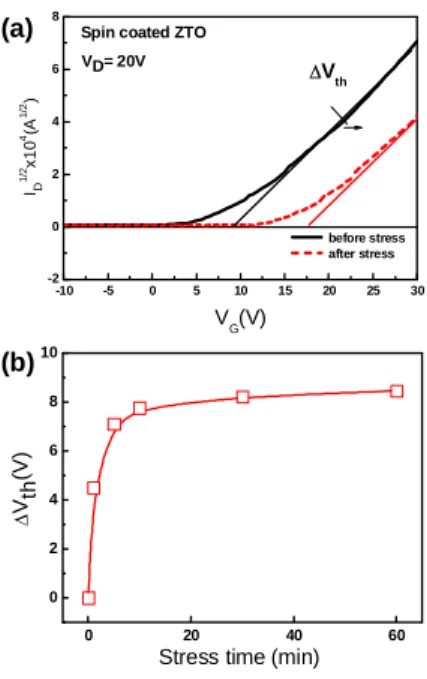
Figure 2a shows the plot of the square root of the drain current as a function of the applied gate bias. After the first gate voltage sweep, the gate electrode was stressed at 20 V for 60 min. Following this, the second gate voltage sweep was performed. The slope of the linear part of the curve, which is proportional to the field effect mobility in the
-20 0 20 40 10-10 10-9 10-8 10-7 10-6 10-5 10-4 10-3 ID (A ) VG = 10V VG = 20V VG = 30V VG = 40V VD (V) VD=20 V ID (A ) VG(V)
Spin coated ZTO
0 20 40 10-12 10-10 10-8 10-6 10-4 VG = 10V VG = 20V VG = 30V VG = 40V VD (V) ID (A ) VD= 20 V ID (A ) VG(V)
Inkjet printed ZTO (a)
(b)
Fig. 1. Typical transfer and output characteristics (insets) of ZTO transistors fabricated by (a) spin-coating and (b) ink-jet printing.
-10 -5 0 5 10 15 20 25 30 -2 0 2 4 6 8
Spin coated ZTO
before stress after stress ID 1/ 2x1 0 4(A 1/ 2) VG(V) ∆Vth VD= 20V 0 20 40 60 0 2 4 6 8 10 ∆ Vth (V)
Stress time (min) (a)
(b)
Fig. 2. (a) ID vs VG plot used to extract the
threshold voltage shift for the spin-coated ZTO-TFT after bias stressing with a gate bias of 20 V for 60 min and (b) the time dependence of the threshold voltage shift as a function of bias stress duration.
P2-109 / Y. Jeong
• IMID 2009 DIGEST
saturation regime, is similar for both curves. The application of positive bias stress results in displacement of the transfer curves in the positive direction, but has no effect on the subthreshold behavior. The variation in ∆Vth as a function of the stress time is presented in Fig. 2b. The ZTO transistors involve a sharp rise in ∆Vth, followed by saturation (~ 8.5 V) within 60 min. The positive Vth shift is then explained by the negative charge screening the applied gate voltage. The lower effective gate bias results in a smaller current flowing through the channel, thus a larger positive voltage is required for the device to turn on and reach saturation.[12]
0 20 40
10-11
10-9
10-7
10-5
Spin coated ZTO
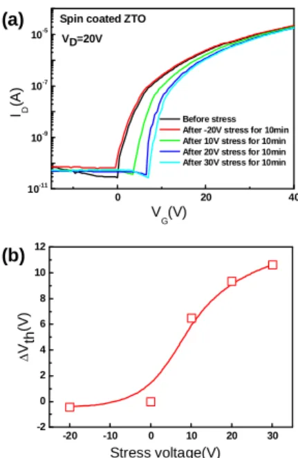
Before stress After -20V stress for 10min After 10V stress for 10min After 20V stress for 10min After 30V stress for 10min ID (A ) V G(V) VD=20V -20 -10 0 10 20 30 -2 0 2 4 6 8 10 12 Stress voltage(V) ∆ Vth (V ) (a) (b)
Fig. 3. (a) Transfer characteristics for the spin-coated ZTO-TFT before and after bias stressing with various gate bias voltages ranging from -20 to 30 V for 10 min and (b) the variation in the threshold voltage shift as a function of the gate bias voltage.
The variation in ∆Vth as a function of the stress voltage is presented in Fig. 3b. However, the application of a negative gate bias stress of -20 V does not change the threshold voltage, and the transfer curve of the stressed TFT overlaps that of the unstressed TFT. This is an indication that when a negative bias is applied to the gate, the transistor channel is depleted of electrons at the channel/dielectric interface and no mobile charges are available for the charge trapping and injection process
from the ZTO channel into the gate dielectric.[13] As a bias stress induced instability mechanism, charge trapping at the channel/ insulator interface has the same effect on the resultant electrical characteristics as charge injection into the insulator. The essential difference between the two is that the energy needed to release the trapped interface charge is much less than that needed to remove the injected charge.[13] For polycrystalline silicon TFTs show similar behavior and this exhibit threshold voltage shift by bias stress. [14] But, in case of polycrystalline silicon TFTs show the change of subthreshold swing value is due to deep state creation. In our study, ZTO based TFTs show only simple translation to uniform direction. And we can explain this situation using charge trapping model.
This positively charged oxygen vacancies can behave as acceptor-like traps that are responsible for a positive shift.[15] The absence of the negative shift indicates that the electron concentration is predominant over the hole concentration in the ZTO.
4. Summary
The stability of solution processed zinc tin oxide (ZTO) transistors under gate bias stress has been studied. The application of positive bias stress results in the displacement of the transfer characteristics in the positive direction without changing the field effect mobility or the subthreshold behavior. It is speculated that oxygen vacancies act as the trapping states.
5. References
[1] E Fortunato, P Barquinha, A Pimentel, A Goncalves, A Marques, L Pereira and R Martins, Thin Solid Films, 487, 205 (2005)
[2] B. Sun and H Sirringhaus, Nano Lett., 5, 12 (2005) [3] G Gu, M Kane, J Doty and A Firester, Appl. Phys. Lett., 87, 243512 (2005)
[4] C Zilker, C Detcheverry and E Cantatore, Appl. Phys. Lett., 79, 1124 (2001)
[5] B Ong, C Li , Y Li, Y Wu and R Loutfy, J. Am. Chem. Soc., 129, 2750 (2007)
[6] D Lee, Y Chang, G Herman and C Chang, Adv. Mater., 19, 843 (2007)
[7] Y Chang, D Lee, G Herman and C Chang, Electrochem Solid State Lett., 10, H135 (2007)
[8] D Kawakami, Y Yasutake, H Nisshizawa and Y Majima, J. Appl. Phys., 45, 1127 (2006)
[9] C Huang, J Tsai, T Teng, C Yang and H Cheng, J. Appl. Phys., 39, 5763 (2000)
P2-109 / Y. Jeong
IMID 2009 DIGEST • [10] K Karim, A Nathan, M Hack and W Milne, IEEE
Electron Device Lett., 25, 188 (2004)
[11] S Jeong, Y Jeong and J Moon, J. Phys. Chem. C, 112, 11082 (2008)
[12] A Suresh and J Muth, Appl. Phys. Lett., 92, 033502 (2008)
[13] A Merticaru and A Mouthaan, Thin Solid Films, 383, 122 (2001)
[14] J Kim, J Choi, S Kim and J Jang, IEEE Electron Device Lett., 25, 182 (2004)
[15] J Park, J Jeong, H Chung, Y Mo and H Kim, Appl. Phys. Lett., 92, 072104 (2008)