Change in the resistivity of Ge-doped Sb phase change thin films grown by chemical
vapor deposition according to their microstructures
Jin-Hyock Kim, Keun Lee, Su-Jin Chae, Il-Keoun Han, Jae-Sung Roh, Sung-Ki Park, Byung Joon Choi,
Cheol Seong Hwang, Eunae Cho, and Seungwu Han
Citation: Applied Physics Letters 94, 222115 (2009); doi: 10.1063/1.3151959 View online: http://dx.doi.org/10.1063/1.3151959
View Table of Contents: http://scitation.aip.org/content/aip/journal/apl/94/22?ver=pdfcov
Published by the AIP Publishing
Articles you may be interested in
Electrical transport phenomena prevailing in undoped nc-Si/a-SiNx:H thin films prepared by inductively coupled plasma chemical vapor deposition
J. Appl. Phys. 114, 073708 (2013); 10.1063/1.4818512
Controlling the resistivity gradient in aluminum-doped zinc oxide grown by plasma-enhanced chemical vapor deposition
J. Appl. Phys. 112, 043708 (2012); 10.1063/1.4747942
Microstructure and resistivity characterization of CuAu I superlattice formed in Cu ∕ Au thin films
J. Vac. Sci. Technol. B 22, 2715 (2004); 10.1116/1.1819899
Microstructure of ultrananocrystalline diamond films grown by microwave Ar–CH 4 plasma chemical vapor deposition with or without added H 2
J. Appl. Phys. 90, 118 (2001); 10.1063/1.1377301
Electrical properties of Ta-doped SnO 2 thin films prepared by the metal–organic chemical-vapor deposition method
Appl. Phys. Lett. 78, 350 (2001); 10.1063/1.1337640
Reuse of AIP Publishing content is subject to the terms at: https://publishing.aip.org/authors/rights-and-permissions. Download to IP: 203.255.172.21 On: Tue, 25 Oct 2016 06:29:13
Change in the resistivity of Ge-doped Sb phase change thin films grown
by chemical vapor deposition according to their microstructures
Jin-Hyock Kim,1,a兲 Keun Lee,1Su-Jin Chae,1Il-Keoun Han,1Jae-Sung Roh,1 Sung-Ki Park,1 Byung Joon Choi,2 Cheol Seong Hwang,2,b兲 Eunae Cho,3 and Seungwu Han3
1Research and Development Division, Hynix Semiconductor, Inc., Icheon-si, Kyoungki-do 467-701, Korea 2Department of Materials Science and Engineering and Inter-University Semiconductor Research
Center, Seoul National University, Kwanak-ku, Seoul 151-742, Korea
3
Department of Physics, Ewha Womans University, Seoul 120-750, Korea
共Received 26 April 2009; accepted 17 May 2009; published online 5 June 2009兲
This study examined the effects of the composition and microstructure on the electric resistivity of Ge-doped Sb phase change thin films grown by cyclic plasma enhanced chemical vapor deposition. Ge and Sb layers were deposited sequentially to form either a GexSby mixture or Ge/Sb
nanolaminated films. While the resistivity of the nanolaminated films was higher, the GexSby
mixture showed a lower resistivity than the pure Sb film. This can be explained by the increase in carrier density of the alloy, as confirmed by first-principles calculations. An abrupt change in resistance accompanying a phase change was observed at⬃210 °C. © 2009 American Institute of
Physics. 关DOI:10.1063/1.3151959兴
Phase change random access memory共PCRAM兲 has at-tracted considerable interest as a candidate for the next gen-eration nonvolatile devices that will meet the need of higher density and operation speed.1 Ternary Ge2Sb2Te5 共GST兲 compounds are widely regarded as suitable phase change materials for PCRAM. However, the relatively long crystal-lization time of GST 共hundreds of nanoseconds兲 limits the operation speed of the PCRAM device compared to other spin-memory device.2 In addition, a confined cell structure where the PC material is formed inside a contact hole is expected to be essential for the next generation PCRAM de-vices because it requires lower switching power.3 In this case, chemical vapor deposition 共CVD兲 should be used to deposit the PC material instead of conventional sputtering because high conformal growth is needed. However, it is quite difficult to control the composition in CVD of GST accurately.4Therefore, a binary PC alloy with a higher crys-tallization speed may be a better choice than ternary alloys in the mass production of devices.
In recent years, Te-free, Sb-based phase change materi-als properly doped with Ge, In, Ga, Sn, and Zn have attracted interest on account of their faster crystallization speed and long term stability.5–8 Because undoped Sb is usually crys-talline over the operation temperature range of PCRAM, dopants should play an important role in enhancing the amorphous phase stability, even though it reduces the crys-tallization speed slightly. Among the various doped Sb-based PC materials, the Ge doped Sb alloy has been studied widely since 1990s. Afonso et al.5 demonstrated that a reversible phase change in Ge0.1Sb0.9can be achieved with a femto- and picosecond laser pulses. In general, the PC material proper-ties, such as amorphous phase stability, crystallization rate, and optical constants are strongly influenced by the material composition. Ge is effective in enhancing the amorphous phase stability because of its high bond strength and
rela-tively high coordination number.7This paper reports the ef-fect of the composition and microstructure on the electric resistivity of Ge–Sb PC materials deposited by cyclic plasma enhanced CVD using a supercycle concept.9
All Ge–Sb films were prepared on thermally grown on SiO2共100 nm兲/Si substrates using Ge关N共CH3兲共C2H5兲2兴4and Sb关N共CH3兲共C2H5兲2兴3 as Ge and Sb precursors, respectively, with the aid of Ar/H2plasma gas at a substrate temperature of 150 ° C. Table Isummarizes the detailed process param-eters. One supercycle for Ge–Sb thin film deposition con-sisted of Ge and Sb subcycles. During the Ge and Sb depo-sition step, the cycles were repeated until the desired thickness of each layer was achieved. One supercycle can be denoted as共Ge:Sb兲=共m:n兲, where m and n are the numbers of Ge and Sb subcycles. The Ge and Sb layers were grown sequentially during a single supercycle, and the thickness of each layer was controlled to fabricate either the mixed 共GexSbyalloy兲 or nanolaminated structures of the Ge–Sb thin
films. The mixed structure was achieved when the number of Ge deposition cycles was not high enough to form a continu-ous and discrete Ge layer. The film thickness was examined by cross-section field-emission scanning electron micros-copy. The film composition was estimated by low-energy electron-induced x-ray emission spectroscopy. The micro-structure of the film was examined by transmission electron microscopy 共TEM兲. The sheet resistance was checked by four-point probe measurements.
a兲Electronic mail: [email protected]. b兲Electronic mail: [email protected].
TABLE I. Deposition conditions.共SCCM denotes standard cubic centime-ters per minute at STP.兲
Condition Ge Sb
Working pressure 2 torr 1.2 torr
Carrier Ar 500 SCCM 500 SCCM
Purge Ar 300 SCCM 300 SCCM
Reactant gas共H2兲 50 SCCM 50 SCCM
Plasma power 50 W 50 W
APPLIED PHYSICS LETTERS 94, 222115共2009兲
0003-6951/2009/94共22兲/222115/3/$25.00 94, 222115-1 © 2009 American Institute of Physics
Reuse of AIP Publishing content is subject to the terms at: https://publishing.aip.org/authors/rights-and-permissions. Download to IP: 203.255.172.21 On: Tue, 25 Oct 2016 06:29:13
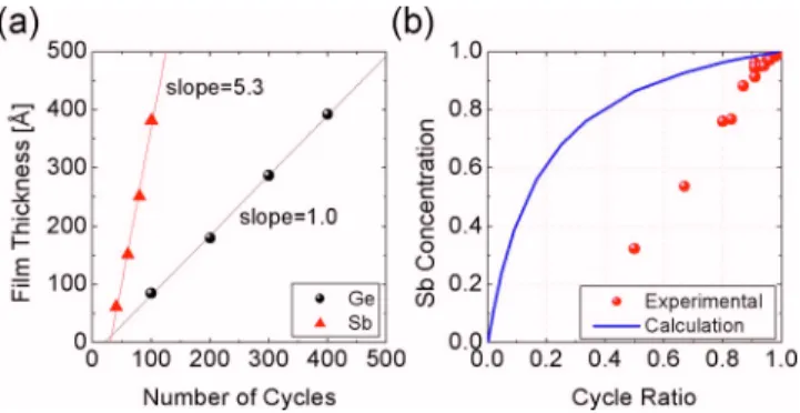
Figure1共a兲shows the dependence of the Ge and Sb film thickness on the number of deposition cycles in the single layer deposition process. The film thickness increased lin-early with increasing the number of deposition cycles. The growth rates of Ge and Sb, which are defined as the slope of the line of best fit, were 1.0 and 5.3 Å/cycle, respectively. The incubation cycles during the initial stage of film growth, where the films do not grow, were⬃20 and ⬃30 cycles for Ge and Sb films, respectively. The resistivity of the Sb film was 293 ⍀, which was calculated from the sheet resistance and film thickness.共Resistivity of bulk Sb=41.7 ⍀ cm.兲 It is possible to control the elemental composition ratio in Ge–Sb thin films by changing the cycle ratio, which is de-fined as n/共m+n兲. Because the growth rate of Sb films was much higher than that of Ge, the expected composition of the Ge–Sb films as a function of the cycle ratio was calculated using Eq.共1兲
Sb concentration = m⫻ GRSb/VSb
n⫻ GRGe/VGe+ m⫻ GRSb/VSb, 共1兲 where GRGe and GRSb are the growth rates of Ge and Sb, respectively, and VGeand VSbare the unit volumes of Ge and Sb, respectively. The VGe and VSb were estimated from the atomic distance to be 36.59 and 28.93 Å3. Figure1共b兲shows the calculation result as a 共blue兲 line.
In contrast to expectations, the Sb concentration in-creased linearly with increasing cycle ratio and was much lower than expected. This suggests that Sb growth decreases with increasing Ge concentration. The more detailed growth behavior of this Ge–Sb alloy film will be reported elsewhere. As the Sb layer thickness grown per pulse of the Sb precursor was much larger than the expected monolayer Sb thickness, it is probable that the Sb material deposited during a single Sb pulse forms a continuous layer structure. How-ever, as the Ge growth rate was only⬃1.0 Å/cycle, the Ge material grown during a single Ge pulse may not form a continuous layer. Whether Ge growth results in a continuous layer or not is critically important for controlling the micro-structure of the film共alloy mixture or nanolaminate兲. There-fore, the minimum number of consecutive Ge pulses that forms a distinctively continuous Ge layer was found in the following manner.
First, a 20 Å thick Ge layer was grown as a seed layer. Sb and Ge layers were then grown alternatively, where the Sb cycle number was fixed to 20 but the Ge cycle number was varied such as 2, 4, and 6 in one sample 关TEM in Fig.
2共a兲兴 and 8, 10, and 15 cycles in the other 关Fig. 2共b兲兴. Ge
appears brighter in TEM than Sb because of the lower atomic weight of Ge. A continuous layer of Ge was formed after⬃4 Ge cycles. The film shows a nanolaminated microstructure when the Ge cycle number was⬎4. However, at a Ge cycle number of 2, the Ge appears to dissolve into the Sb film resulting in a homogeneously mixed GexSbyalloy. Once the
continuous Ge layer was formed, there appears to be less Ge dissolution into the Sb layer as will be shown later.
The Ge concentration largely affects the microstructure and electrical properties of the GexSby alloy and Ge–Sb
nanolaminates. Figure2共c兲shows the changes in film tivity, which was estimated by multiplying the sheet resis-tance by the film thickness, as a function of the cycle ratio. Here, the sequence of pulse cycles was varied to achieve either a mixture film共Ge cycle: Sb cycle=1:n兲 or nanolami-nate films 关共Ge cycle: Sb cycle=5:n兲兴, while the total Sb cycle number was fixed to 100. Generally, the films showed very high resistivity when the cycle ratio was ⬍0.8 for 1:n process and ⬍0.67 for 5:n process due to the amorphous structure of the film关Fig.4共b兲兴. The Ge concentrations in the film with a cycle ratio of 0.8 for the 1 : n process and that for the film with a cycle ratio of 0.67 for the 5 : n process were ⬃23% and 46%, respectively. There are two interesting find-ings from Fig. 2共c兲. First, the films have quite different re-sistivity, even though the cycle ratio was the same 共approxi-mately for 0.8 of cycle ratio, n was 4 and 20兲 for the two processes. Second, the films grown by the 1 : n process showed lower resistivity than the pure Sb film when the cycle ratio was⬎0.9. This was quite unexpected because Ge may act as an impurity in a Sb film and scatter the carriers, which would increase the resistivity.
The first phenomenon can be understood from the mi-crostructural features shown in Fig.2共a兲. When the Ge cycle number was 1, the film must be a homogenous mixture. Therefore, all the incorporated Ge works as a dopant that enhances the amorphousness of Sb, which makes the film with a Ge concentration of only 23%共cycle ratio=0.8兲 amor-phous. However, for the 5 : n process, most of the Ge atoms is present as a separate Ge layer, which diminishes the dop-ing effect. Therefore, even with the same cycle ratio of 0.8, the film was already crystallized and showed much lower resistivity than the film formed by the 1 : n process. In order to understand the second phenomenon, the energy band structure of Ge-doped Sb was examined by the first-principles calculations using VASP.10 The projector-augmented-wave pseudopotentials were used to describe the FIG. 1.共Color online兲 共a兲 variation in the thicknesses of Ge and Sb films as
a function of the number of cycles and共b兲 variation in the Sb concentration as a function of the cycle ratio.
FIG. 2. 共Color online兲 Cross-section TEM images of the film grown with the sequence of 共a兲 Ge共20兲–Sb–Ge共2兲–Sb–Ge共4兲–Sb–Ge共6兲–Sb and 共b兲 Ge共20兲–Sb–Ge共8兲–Sb–Ge共10兲–Sb–Ge共15兲–Sb, where the number in paren-thesis shows the Ge cycle number. The number of Sb cycles was fixed to 20. 共c兲 Changes in resistivity of the Ge–Sb alloy as a function of the cycle ratio.
222115-2 Kim et al. Appl. Phys. Lett. 94, 222115共2009兲
Reuse of AIP Publishing content is subject to the terms at: https://publishing.aip.org/authors/rights-and-permissions. Download to IP: 203.255.172.21 On: Tue, 25 Oct 2016 06:29:13
electron-ion interactions.11 The exchange-correlation ener-gies between electrons were calculated within the general-ized gradient approximation.12The energy cutoff was chosen to be 250 eV and the k-points were sampled on 4⫻4⫻3 regular meshes for a unit super cell共see below兲. The atomic positions were relaxed until the Hellmann–Feynman force on each atom was reduced to within 0.02 eV/Å. To calculate the defect structure, the hexagonal unit cell of Sb was expanded to an orthorhombic supercell with dimensions of 8.78 ⫻7.59⫻11.43 Å3. A substitutional Ge atom was considered to simulate Ge-doped Sb thin films. 共The interstitial defect was also examined but the formation energy was ⬃1.0 eV higher than that for a substitutional one.兲 Figs.3共a兲and3共b兲
show the relaxed structures and computed density of states 共DOS兲, respectively. The DOS of crystalline Sb showed a dip at the Fermi level, which is indicative of semimetallic properties.13 In the presence of defects, the DOS profile did not change much but the Fermi level rigidly shifts down. This is due to the lower number of valence electrons in Ge than Sb. As a result, the DOS increases at the Fermi level because the Fermi level was positioned at the dip of the DOS for crystalline Sb. This is in good agreement with the experi-mental observations of lower resistivity in the Ge-doped Sb thin films.
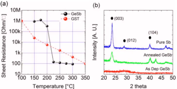
Figure 4共a兲 shows the change in sheet resistance of a Ge0.23Sb0.77mixture film as a function of the annealing tem-perature. The resistance decreased 104 times upon crystalli-zation 关Fig. 4共b兲兴 at ⬃200–220 °C. The PC behavior achieved from the Ge2Sb2Te5 film grown by sputtering is also included for comparison. The GST showed a gradual change in the resistance with temperature even though the eventual resistance ratio was similar. Figure4共b兲 shows that the crystallization of a Ge0.23Sb0.77 mixture is accomplished by phase separation of Sb metal from the alloy. The estima-tion of crystallizaestima-tion speed and reversible PC characteristics
will be reported in a subsequent report using an integrated cell structure.
B.J.C. and C.S.H. acknowledge the support of the Na-tional Research Program for the Nano Semiconductor Appa-ratus Development sponsored by the Korea Ministry of Knowledge and Economy, and World Class University pro-gram through the Korea Science and Engineering Foundation funded by the Ministry of Education, Science and Technol-ogy 共Contract No. R31-2008-000-10075-0兲.
1Y. N. Hwang, S. H. Lee, S. J. Ahn, S. Y. Lee, K. C. Ryoo, H. S. Hong, H.
C. Koo, F. Yeung, J. H. Oh, H. J. Kim, W. C. Jeong, J. H. Park, H. Horri, Y. H. Ha, J. H. Yi, G. H. Koh, G. T. Jeong, H. S. Jeong, and K. Kim, Tech. Dig. - Int. Electron Devices Meet 2003, 893.
2C. Chappert, A. Fert, and F. N. V. Dau,Nature Mater. 6, 813共2007兲. 3J. I. Lee, H. Park, S. L. Cho, Y. L. Park, B. J. Bae, J. H. Park, J. S. Park,
H. G. An, J. S. Bae, D. H. Ahn, Y. T. Kim, H. Horii, S. A. Song, J. C. Shin, S. O. Park, H. S. Kim, U-I. Chung, J. T. Moon, and B. I. Ryu, Tech. Dig. VLSI Symp. 2007, 102.
4J. Choi, S. Choi, Y. C. Shin, C. S. Hwang, Y. J. Kim, Y. J. Son, and S. K.
Hong,Chem. Mater. 19, 4387共2007兲; B. J. Choi, S. Choi, Y. C. Shin, C.
S. Hwang, J. W. Lee, J. Jeong, Y. J. Kim, S.-Y. Hwang, and S. K. Hong,J. Electrochem. Soc. 154, H318共2007兲.
5C. N. Afonso, J. Solis, F. Catalina, and C. Kalpouzos,Appl. Phys. Lett. 60, 3123共1992兲.
6L. V. Pieterson, M. V. Schijndel, J. C. N. Rijpers, and M. Kaiser, Appl.
Phys. Lett. 83, 1371共2003兲.
7L. V. Pieterson, M. H. R. Lankhorst, M. V. Schijndel, A. E. T. Kuiper, and
J. H. J. Roosen,J. Appl. Phys. 97, 083520共2005兲.
8T. J. Park, D. H. Kim, S. J. Park, S. Y. Choi, S. M. Yoon, K. J. Choi, N. Y.
Lee, and B. G. Yu,Jpn. J. Appl. Phys., Part 2 46, L543共2007兲. 9J. H. Kim, J. Y. Kim, and S. W. Kang,J. Appl. Phys.97, 093505共2005兲. 10G. Kresse and J. Hafner,Phys. Rev. B 47, 558共1993兲.
11P. E. Blochl,Phys. Rev. B 50, 17953共1994兲.
12J. P. Perdew, K. Burke, and M. Ernzerhof, Phys. Rev. Lett. 77, 3865
共1996兲.
13X. Gonze, J.-P. Michenaud, and J.-P. Vigneron,Phys. Rev. B 41, 11827
共1990兲. FIG. 3. 共Color online兲 共a兲 Relaxed structure of Ge-doped Sb and 共b兲 The
DOS for the crystalline and Ge-doped Sb.
FIG. 4.共Color online兲 共a兲 Changes in the sheet resistance of the Ge–Sb film as a function of the annealing temperature共30 s in air兲 and 共b兲 x-ray dif-fraction pattern of the films. In共a兲 the data for sputtered Ge2Sb2Te5is also
shown for comparison.
222115-3 Kim et al. Appl. Phys. Lett. 94, 222115共2009兲
Reuse of AIP Publishing content is subject to the terms at: https://publishing.aip.org/authors/rights-and-permissions. Download to IP: 203.255.172.21 On: Tue, 25 Oct 2016 06:29:13