P1-41 / E. J. Jeon
IMID 2009 DIGEST •
Abstract
Optically compensated bend (OCB) mode has intrinsic characteristics such as wide viewing angle and fast response time. However, in order to operate the OCB mode in bend state, this device needs quick transitions from the initial splay state to bend state. In this paper, we proposed OCB mode with initially bend state using reactive mesogen (RM) monomer for surface polymer stabilization. The device shows continuous reorientation of the LC with applied field and a very fast response time.
1. Introduction
Nowadays, twisted nematic (TN)1-2 liquid crystal displays (LCDs) are widely used for portable displays such as monitors, notebook computers and mobile phones because they have low cost, lower power consumption and high light efficiency. However, the TN-LCDs have intrinsic problems such as slow response time, and narrow viewing angle. To overcome narrow viewing angle problems, new LC modes are proposed such as in-plane switching (IPS)3, multi-domain vertical alignment (MVA)4, fringe-field switching (FFS)5. But, these modes do not have fast response time. The one method that overcomes this demerit is to use the LCD mode like optically compensated bend (OCB)6 mode. Especially, OCB mode has come into the spotlight because of requirements for fast response time and wide viewing angle characteristics among various LC modes. This mode shows fast response time due to flow acceleration effects and relatively wide viewing angle characteristics due to help of self compensation effect.
In this paper, we proposed OCB mode with initially bend state using UV curable reactive mesogen (RM) monomer7-8. We analyzed that the polymerized RM monomer affected transitions from the initial splay
state to bend state.
2. Experimental
Figure 1 shows chemical structure of UV curable RM monomer (RM257, Merck Co., Ltd) used in proposed OCB mode. It was cured by UV light (365nm, 90mW/cm2). In this experiment, we coated homogeneous alignment layer on the indium tin oxide (ITO) coated glass substrates. Homogeneous alignment layer are rubbed as parallel directions. The LCs in the OCB mode have ∆n of 0.099 and ∆ε of 8.1.
O H3C O O O O O O O O O O H3C O O O O O O O O O
Figure 1. Chemical Structure of UV curable RM
monomer used in proposed OCB mode
Figure 2 shows schematic diagram of the processes for fabricating the OCB mode with defined pretilt angles at the substrate by UV curable RM monomer. In a parallel rubbed cell, the RM monomer is aligned homogeneously along the LC layer due to the use of homogeneous alignment layers on both substrates, as shown in figure 2(a) The vertical field over critical voltage (voltage that shows a bend state) reorients LCs to bend state. At this time, the cell is exposed to UV light and thus the monomers are polymerized with a constant tilt angle at the surfaces, as shown in figure 2(b). Consequently, LCs maintain bend state without applying voltage because of polymerized RM monomer, as shown in figure 2(c).
Realization of Optically Compensated Bend State using
Surface Polymer Stabilization
E. J. Jeon, B. G. Kang, D. W. Kwon, Y. J. Lim, M. -H. Lee and S. H. Lee
Dept. of Polymer Nano•Science and Engineering, Chonbuk National University, Chonju, Chonbuk, 561-756, Korea
Tel.: 82-63-270-2343, E-mail: [email protected]
P1-41 / E. J. Jeon • IMID 2009 DIGEST UV Glass ITO LC RM monomer (a) (b) (c) UV UV UV Glass ITO LC RM monomer Glass ITO LC RM monomer (a) (b) (c)
Figure 2. Schematic diagram of the processes for fabricating the proposed OCB mode with defined pretilt angles at the substrate surfaces: (a) initial splay state, (b) UV curing at applying voltage, and (c) forming new pretilt angle at surface
Figure 3 shows initial orientation of LC molecules according to applied voltage and concentration of RM monomer. In the conventional paper7, over 4 wt% RM monomer is mixed into the LCs to form initial bend state. However, we formed initial bend state by RM monomer under 2 wt% in this paper. Conventionally8, 10 V is applied when the LCs include 2 wt% RM monomers but bend state are formed at 4 V in this paper. Accordingly, we confirmed stabilizing bend state by low concentration and low applied voltage in this paper. 0.0 0.5 1.0 1.5 2.0 2.5 0 5 10 15 20 25 Ap p lie d Vo ltag e (v ) Concentration of RM monomer (%) X O O O O X X X X
O: Completely bend X: twist and/or splay
0.0 0.5 1.0 1.5 2.0 2.5 0 5 10 15 20 25 Ap p lie d Vo ltag e (v ) Concentration of RM monomer (%) X O O O O X X X X 0.0 0.5 1.0 1.5 2.0 2.5 0 5 10 15 20 25 Ap p lie d Vo ltag e (v ) Concentration of RM monomer (%) X O O O O X X X X
O: Completely bend X: twist and/or splay
Figure 3. Orientation of liquid crystal molecules according to applied voltage and concentration of RM monomer
3. Results and discussion
Figure 4 shows measured voltage-dependent transmittance value in normal OCB mode and proposed OCB mode. The proposed OCB mode, which has 2 wt% RM monomer in LCs, is UV cured at 4 V. The electrical properties of normal OCB and proposed OCB modes for measure used LCMS-200 in Sesim. As shown in figure 4, normal OCB mode is in a bend state when critical voltage is over 1.5 V. Proposed OCB mode is initially in a bend state owing to polymerized RM monomer. Accordingly, the proposed OCB mode is possible to operate without critical voltage because polymerized RM monomer formed surface pretilt angle. Although the proposed OCB mode has not shown complete dark state at applied voltage, we can overcome the problems by using multiple optical compensation films9,10.
0 2 4 6 8 10 0.0 0.5 1.0 1.5 2.0 2.5 3.0 3.5 4.0 4.5 Trans m it ta nce (a .u.) Voltage(V)
Normal OCB mode Proposed OCB mode bend 0 2 4 6 8 10 0.0 0.5 1.0 1.5 2.0 2.5 3.0 3.5 4.0 4.5 Trans m it ta nce (a .u.) Voltage(V)
Normal OCB mode Proposed OCB mode bend
Figure 4. Measured transmittance value according to applied voltage in normal OCB and proposed OCB modes
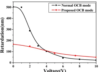
Figure 5 shows retardation value of normal OCB mode and proposed OCB mode according to applying voltage. The electrical properties of normal OCB and proposed OCB modes for measure used REMS-150 in Sesim. Normal OCB mode is initially in a splay state and has high retardation value 540nm at initial state which is decreased steeply according to applying voltage. However, proposed OCB mode is initially in a bend state. The retardation value from 0 V to 10V is decreased respectively from 167nm to 49nm gradually as shown in figure 5. One demerit of the proposed device is that the retardation change ratio is not big enough so light efficiency will be sacrificed.
P1-41 / E. J. Jeon IMID 2009 DIGEST • 0 2 4 6 8 10 0 100 200 300 400
500 Normal OCB mode Proposed OCB mode
Retar d ati on(n m ) Voltage(V) 0 2 4 6 8 10 0 100 200 300 400
500 Normal OCB mode Proposed OCB mode
Retar d ati on(n m ) Voltage(V)
Figure 5. Measured voltage-dependent retardation value in normal OCB and proposed OCB modes
The pretilt variation has an effect on capacitance of LC cell. Accordingly, we measured capacitance values of fabricated OCB mode to confirm pretilt angle of it, using LCR METER in Agilent Technologies. The definition is as follows in terms of the capacitance.
0
>
−
=
∆
×
=
×
=
−
=
∆
⊥ ⊥ ⊥ ⊥ε
ε
ε
ε
ε
ll ll ll lld
A
C
d
A
C
C
C
C
(1)where A, d and ε are the area and cell gap and dielectric constants of LC, respectively. Because A and d were fixed, a capacitance value only depends on tilt angle of LC. Positive LC has higher dielectric constant with parallel direction to electric field than with perpendicular direction to electric field. The proposed OCB mode has higher capacitance values at no applied voltage because of high pretilt angle.
Figure 6 shows measured capacitance by applying AC voltage in normal OCB with initial splay state and proposed OCB initial bend state modes. In normal OCB mode, LCs are initially homogeneous aligned and then the LCs tilt up to perpendicular substrate at 10 V. Phase transition of LC from splay to bend contributed the sudden change of capacitance values(∆C). The LCs are high pretilt angle in proposed OCB mode by polymerized RM monomers at no applied voltage. So, capacitance of proposed OCB mode is higher than normal OCB mode at 0 V. At 10 V, capacitance of proposed OCB mode is lower
than normal OCB mode because LCs of near the surface are not move by applying voltage.
0 2 4 6 8 10 1.5 2.0 2.5 3.0 3.5 4.0 4.5 5.0 5.5 C apa ci tn ac e ( nF ) Voltage (V)
Normal OCB mode Proposed OCB mode bend splay 0 2 4 6 8 10 1.5 2.0 2.5 3.0 3.5 4.0 4.5 5.0 5.5 C apa ci tn ac e ( nF ) Voltage (V)
Normal OCB mode Proposed OCB mode bend
splay
Figure 6. Measured capacitance by applying AC voltage in normal OCB and proposed OCB modes
The LC director’s response time of an LC cell is described as follows: eff 2 2 2 2 0 2 ) (
K
d V V d off on Cπ
τ
ε
ε
τ
γ γ=
−
=
∆ (2)where γ, K and d are the rotational viscosity, elastic constant and cell gap, respectively. V is the applied voltage, and, VC is threshold voltage. The response
time of OCB mode for measure used LCMS-200 in Sesim.
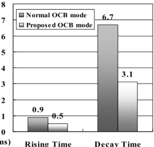
Figure 7 shows measured response time in normal OCB and proposed OCB modes. The rising and decaying times of proposed OCB mode are faster than that of normal OCB mode by 0.4 ms and 3.6 ms, respectively.
The first reason for decreasing response time of the proposed OCB mode is that the LCs are initially bend by RM monomer. In on and off state of LC cells, reorientation path of the LC directors of the proposed OCB mode is less than normal OCB mode with initial splay state because pretilt angle of the propsed OCB mode is 45°. The second reason of fast response time of proposed device is due to the smaller cell gap as the response time is inversely proportional to the d2. The cell gaps of normal OCB and proposed OCB modes are about 5.1um and 4.9um respectively. Hence the
P1-41 / E. J. Jeon
• IMID 2009 DIGEST
cell gap of proposed OCB mode is over 0.1um smaller than normal OCB mode as RM monomers are polymerized at the surface. Response time of the proposed device is observed to decrease by 10%.
0.9 6.7 0.5 3.1 0 1 2 3 4 5 6 7 8
Rising Time Decay Time (ms)
Normal OCB mode Proposed OCB mode
Figure 7. Measured Response time in normal OCB and proposed OCB modes.
4. Summary
The conventional OCB mode always requires transition from the initial splay state to bend state. We proposed the OCB mode with initially bend state using UV curable RM monomer for surface polymer stabilization and thus continuous reorientation of the LC with applied field is observed with a very fast response time.
Acknowledgement
This research was financially supported by the Ministry of Commerce, Industry and Energy (MOCIE) and Korea Industrial Technology Foundation (KOTEF) through the Human Resource Training for Regional Innovation.
5. References
1. M. Schadt, W. Helfrich, Appl. Phys. Lett., 18, p.127 (1971).
2. S. H. Hwang, Y. J. Lim, M. -H. Lee, S. H. Lee, G. D. Lee, H. Kang, K. J. Kim and H. C. Choi, Curr. Appl. Phys., 11, p.690 (2007).
3. M. Oh-e, M. Ohta, S.Aratani, K. Kondo, Proc. of the 15th IDRC, p.577 (1995).
4. A. Takeda, S. Kataoka, T. Sasaki, H. Chida, H.
Tsuda, K. Ohmuro, Y. Koike, T. Sasabayashi, and K. Okamoto, SID ’98 Digest, 29, p.1077 (1998).
5. S. H. Lee, S. L. Lee, and H. Y. Kim, Appl. Phys. Lett., 73, p.2881 (1998).
6. P. J. Bos, P. A. Johnson and K. R. Koehler- Beran, SID ’83 Digest, 27, p.30 (1983).
7. R. Hasegawa, Y. Kidzu, I. Amemiya, S. Uchikoga, H. Wakemoto, SID '07 Digest, p.995 (2007).
8. T. -J. Chen, C. -C. Chen, J. -J. Wu, and C. -H. Sun, Jpn. J. Appl. Phys., 46, p.4203 (2007).
9. S. -H. Chang and C. -L. Pan, Proc. of the 11th International Display Workshops, p.137 (2004). 10. T. -J. Chang and P. -L. Chen, Proc. of the 10th