APL Mater. 5, 046106 (2017); https://doi.org/10.1063/1.4981646 5, 046106
© 2017 Author(s).
ZnO nanotube waveguide arrays on
graphene films for local optical excitation
on biological cells
Cite as: APL Mater. 5, 046106 (2017); https://doi.org/10.1063/1.4981646
Submitted: 06 February 2017 . Accepted: 07 April 2017 . Published Online: 25 April 2017
Hyeonjun Baek, Hankyul Kwak, Minho S. Song, Go Eun Ha, Jongwoo Park, Youngbin Tchoe, Jerome K. Hyun, Hye Yoon Park, Eunji Cheong, and Gyu-Chul Yi
COLLECTIONS
This paper was selected as an Editor’s Pick
ARTICLES YOU MAY BE INTERESTED IN
Scalable ZnO nanotube arrays grown on CVD-graphene films
APL Materials 4, 106104 (2016); https://doi.org/10.1063/1.4964490
A nonvolatile memory device with very low power consumption based on the switching of a standard electrode potential
APL Materials 5, 046105 (2017); https://doi.org/10.1063/1.4980031
Evidence for oxygen vacancy manipulation in La1/3Sr2/3FeO3−�� thin films via voltage controlled solid-state ionic gating
ZnO nanotube waveguide arrays on graphene films
for local optical excitation on biological cells
Hyeonjun Baek,1Hankyul Kwak,2Minho S. Song,1Go Eun Ha,2
Jongwoo Park,1Youngbin Tchoe,1Jerome K. Hyun,3
Hye Yoon Park,4Eunji Cheong,2,aand Gyu-Chul Yi1,a
1Department of Physics and Astronomy, Institute of Applied Physics (IAP), Research Institute of Advanced Materials (RIAM), Seoul National University, Seoul 08826, South Korea
2Department of Biotechnology, College of Life Science and Biotechnology, Yonsei University, Seoul 120-749, South Korea
3Department of Chemistry and Nanoscience, Ewha Womans University, Seoul 120-750, South Korea
4Department of Physics and Astronomy, Seoul National University, Seoul 08826, South Korea (Received 6 February 2017; accepted 7 April 2017; published online 25 April 2017)
We report on scalable and position-controlled optical nanoprobe arrays using ZnO nan-otube waveguides on graphene films for use in local optical excitation. For the waveg-uide fabrication, position-controlled and well-ordered ZnO nanotube arrays were grown on chemical vapor deposited graphene films with a submicron patterned mask layer and Au prepared between the interspace of nanotubes. Mammalian cells were cul-tured on the nanotube waveguide arrays and were locally excited by light illuminated through the nanotubes. Fluorescence and optogenetic signals could be excited through the optical nanoprobes. This method offers the ability to investigate cellular behavior with a high spatial resolution that surpasses the current limitation. © 2017 Author(s). All article content, except where otherwise noted, is licensed under a Creative Commons Attribution (CC BY) license (http://creativecommons.org/licenses/by/4.0/). [http://dx.doi.org/10.1063/1.4981646]
High spatial resolution optical excitation is of great importance for improved understanding and fine control of living systems.1–3 For example, it enables fundamental probing techniques in opto-genetics4,5 and uncaging of neurotransmitters6,7 for accurate spatial mapping of neuronal activity. Single molecule fluorescence in biological systems requires highly localized optical excitation.8,9 Several techniques have been used to reduce the excitation volume, including laser focusing,10,11two photon excitation,12,134Pi,14image interference and incoherent interference illumination microscopy (I5M),15and near field excitation.16,17However, most of these methods involve complex and bulky optical systems. Additionally, localized excitation based on evanescent fields is spatially limited to probing the surface of cells. To improve the spatial resolution in optical microprobing, optical probes based on nanostructures have been reported.18–21In these approaches, nanostructures were used as optical waveguides for illuminating a cell. The excitation volume can be highly localized near the tip of the nanostructures by optical confinement, without using additional optical components. The tight attachment between nanostructures and cells cultured on them enables strong optical interac-tions. Scalable, one-dimensional nanostructured arrays are essential for investigating numerous cells simultaneously. Furthermore, both positional and spacing control of the nanostructures is critical for optical nanoprobe applications. Here, we report on scalable and position-controlled optical nanoprobe arrays using ZnO nanotube waveguides on graphene films for use in local optical illumination.
The nanorod waveguides as optical nanoprobe arrays for living cells were fabricated using position-controlled and well-ordered ZnO nanotube arrays grown on chemical vapor deposited (CVD) graphene films.22Figure1(a)represents a schematic of the fabrication processes of ZnO nanotube
aAuthors to whom correspondence should be addressed. Electronic addresses:[email protected]and[email protected]
046106-2 Baek et al. APL Mater. 5, 046106 (2017)
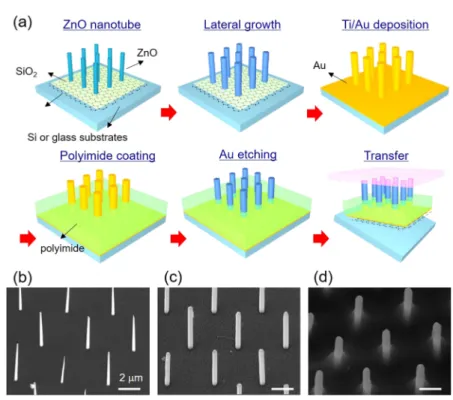
FIG. 1. Fabrication process for ZnO nanotube waveguide arrays. (a) Schematic illustrations of the fabrication of ZnO nanotube waveguide arrays on graphene films. ((b)–(d)) FESEM images of ZnO nanotubes grown on CVD graphene films after vertical growth (b), after lateral growth (c), and after polyimide coating and oxygen plasma ashing (d). FESEM images were obtained at a tilt angle of 30◦.
waveguide arrays on CVD-grown graphene films. Before growing the nanorods, a SiO2 growth
mask layer was coated on the graphene films. Conventional e-beam lithography and subsequent dry and wet etching techniques were used to make a submicron-hole array pattern on SiO2-coated
CVD graphene films.22Then vertically aligned nanotubes were grown selectively along the pattern edges. Accordingly, this method enables us to control the positions and diameters of nanotubes. The corresponding field-emission scanning electron microscopy (FESEM) image is shown in Fig.1(b). The nanotube diameter was 200–300 nm at the base, and the length was 7–8 µm. The walls of nanotubes were too thin to support light propagation sufficiently. Therefore, additional lateral growth was performed at a low temperature of 470◦C and a reactor pressure of 8 Torr, whereas nanorod growth
was performed at 650◦C and 3 Torr. Lateral growth increased the nanotube outer radius from 200 to
460 nm, as shown in Fig.1(c). The SiO2masking layer promoted preferential nucleation and growth of
ZnO on ZnO nanotube surface. Then, a 30-nm-thick Al2O3layer was coated on ZnO nanotubes using
atomic layer deposition. The Al2O3layer protects ZnO from chemical reactions during subsequent
processes and enhances the mechanical stability. Next, Ti/Au (20/140 nm) bilayers were deposited on the entire sample at an incident flux angle of 22◦while rotating the substrate to create an opaque background. Subsequently, a polyimide layer was spin-coated and etched using an oxygen plasma asher to expose the metal-coated nanotube tips, as shown in Fig.1(d). The exposed Au layer on the nanorod tips was then removed using wet chemical etching, which allows light transmission only through the nanotubes. The nanotubes grown on graphene films were easily transferable onto various foreign substrates due to the weak van der Waals bonding between graphene films and the original substrates.22,23In this work, the ZnO nanotube waveguide arrays on graphene films were transferred onto a transparent glass substrate for backside illumination. We believe that this transferability would be used to advance other applications, such as flexible nanoprobe arrays for in vivo studies.
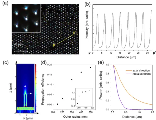
Light transmission through nanotube waveguide arrays was explored using a white light emitting diode (LED) lamp as a backside illumination source. Figure2(a)shows an optical microscope image of the light transmitted through the metal-deposited nanotube arrays. Light is seen to selectively transmit through the nanotubes. The magnified image in the inset clearly shows that light transmission was tightly confined to the nanotubes. The light intensity along the line in the microscope image (p–p’) of
FIG. 2. Light transmission through ZnO nanotube waveguide arrays. (a) An optical microscope image of light transmitted through metal-deposited nanotube arrays in a hexagonal pattern. (b) Plot of light intensity along the line (p–p’) in (a). (c) Optical power distribution for a nanotube with an outer radius of 300 nm. (d) Optical power propagation efficiency through nanotubes having different radii. The inset shows the plot in logarithmic scale. (e) Plot of normalized optical power as a function of distance from the brightest spot after propagation in the axial and radial directions.
Fig.2(b)shows uniform light transmission through the nanotubes, indicating excellent homogeneity in optical throughput among the nanotube waveguides.
Finite-difference time-domain (FDTD) simulations were employed to investigate light propa-gation through nanotube waveguides inside a cellular body. A vertically standing ZnO nanotube on metal coated glass was considered. The simulation used a background refractive index of 1.37 to model a cellular environment.24 The experimental nanotubes were closed at the tip; therefore, the simulated nanotube was modeled with a 200 nm thick solid disk at the tip. The inner radius of the nanotube was set to 100 nm, and the outer radius was varied from 150 to 500 nm to explore the thickness dependence. Height of the nanotube was set to 2 µm. For light illumination, a continuous plane wave source with a wavelength of 470 nm was placed below the surface of the glass substrate. Figure2(c)depicts the calculated optical power distribution in a ZnO nanotube waveguide with an outer radius of 300 nm. Light was propagated through the nanotube and diffracted into the opening at the tip. Interestingly, light exited the nanotube from the axial center, despite propagating through the shell of the hollow structure. The optical power propagation efficiency was calculated by dividing the power transmission through the nanotube by the cross-sectional area of the nanotube, normal to the propagation direction (see experimental). Nanotubes with an outer radius above 300 nm showed efficiencies of more than 10%, whereas nanotubes with an outer radius of 150 nm showed efficiencies as low as 0.26% due to the thin walls (Fig.2(d)).
Optical power intensities along the axial and radial directions of the nanotubes were used to assess the spatial distribution of light exiting the nanotube tips and to calculate the illumination volume. Figure2(e)shows a plot of optical power as a function of distance in the axial and radial directions from the brightest point after the light exits a nanotube with an outer radius of 300 nm. For comparison, the optical powers were normalized to the value at the brightest point. The illumination volume was 150 nm in the radial direction, where the power of transmitted light is half of the maximum power, and 600 nm in the axial direction, where the power of transmitted light is reduced by 10 1compared
046106-4 Baek et al. APL Mater. 5, 046106 (2017)
with the maximum power. This illumination is comparable to that of a conventional focal volume generated by a high NA ultraviolet objective lens, indicating that the nanotube waveguide can provide a highly localized excitation volume.25Note that the ZnO nanotube showed better light propagation and localization than a SiO2nanorod having the same outer radius. Despite its hollow structure, the
higher refractive index of the ZnO nanotube improved the light confinement. This result highlights the benefits of using high-index semiconductor nanostructures as waveguides.
Mammalian cells (HeLa and U2OS) were cultured on nanotube waveguide arrays to explore cellular illumination. Before plating the cells, fibronectin was coated on the nanotubes for better attachment of the cells onto the nanotube surface. Figure3(a)and its inset show FESEM images of HeLa cells cultured on nanotube waveguide arrays. Cells were spread onto the nanotube arrays wrapping them, and the cell bodies protruded from the nanotubes, confirming the tight adhesion of the cell membranes to the nanotubes. The inset shows a space between the cell membrane and the underlying substrate, indicating that the cells were mainly attached to the upper portion of the nanotubes. Furthermore, cells extended across the nanotubes, confirming the affinity between the cells and nanotubes. Figure 3(b) shows a fluorescence image of HeLa cells stained with calcein AM dye (green) and grown on nanotube waveguide arrays. An image of light transmitted through the nanotubes (shown as white dots) was merged with the fluorescence image to visualize the cells grown on the nanotube arrays.
Fluorescent dyes (calcein AM) in the cells were excited through the nanotubes to demonstrate the use of nanotube waveguide arrays for local cellular illumination. Figure4(a)shows a schematic of fluorescence excitation in cells using a nanotube waveguide array. A laser beam was illuminated from the backside of the nanotube array for local fluorescence excitation. Figure4(b)represents laser light transmitted through the nanotube waveguides. Light transmission could be observed only through the nanotubes. Prior to fluorescence excitation through the nanotube waveguides, an epifluorescence image was obtained for comparison. An LED lamp was used as the excitation source and illuminated the array from the bottom side, as shown in Fig.4(a). In the epifluorescence image (Fig.4(c)), the nanotube sites can be seen as dark spots, likely due to the reduced dye content at each nanotube and stronger reflection from the bare Au background. Figure4(d)shows the fluorescence image of cells grown on the nanotube arrays and excited by the nanotube waveguide illumination. Finally, Fig.4(e)shows an epifluorescence image (Fig.4(c)) overlaid with the fluorescence image (Fig.4(d)). Fluorescence was localized to the areas where cells grew on the nanotubes. No emission was observed for cells grown outside the nanotube arrays, indicating that the localized fluorescence was excited by the light transmitted through the nanotube waveguides. However, some cells located near the nanotube arrays showed dim fluorescence, presumably due to scattered light.
Fluorescence excitation by a single nanotube was demonstrated using a focused laser beam. Figures 5(a)–5(c)show fluorescence images (red color) excited by a single nanotube at different positions by changing the position of focused laser beam. The fluorescence images were merged with the epifluorescence image. Fluorescence emission from single points was observed clearly. This
FIG. 3. SEM and epifluorescence images of cells grown on nanotubes. (a) FESEM and (b) epifluorescence images of cells grown on nanotube arrays. The inset in (a) shows a high magnification SEM image.
FIG. 4. Fluorescence excitation using nanotube waveguides. (a) A schematic illustration of fluorescence excitation using nanotube illumination. (b) Laser light transmitted through nanotube arrays. (c) An epifluorescence image of HeLa cells cultured on nanotube arrays. (d) A fluorescence image of excitation by light transmitted through nanotubes. (e) A merged image of (c) and (d).
approach enables selective and serially localized optical excitation on specific locations of cells, such as the dendritic spine of a neuron.
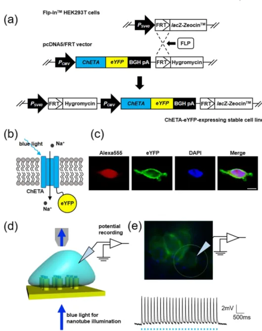
We also demonstrate optical illumination through nanotube arrays for optogenetic stimulation. Human embryonic kidney 293 (HEK293T) cells expressing ChETA which is a light gated cation channel were generated (Fig.6(a)) and cultured on nanotube waveguide arrays. The ChETA-EYFP fusion proteins (Fig.6(b)) were highly expressed on the membrane of HEK293T cells confirmed with EYFP expression with confocal images (Fig.6(c)). To activate the ChETA in adherent HEK cells, a 473 nm laser beam (40 mW/mm2) illuminated the backside of the nanotube waveguides (Fig.6(d)). ChETA-induced potentials by illumination of laser beam through nanotubes were measured using the whole cell patch clamp. The recorded cell is indicated by a circle in the fluorescence image of HEK
FIG. 5. Localized fluorescence excitation using a single nanotube. ((a)–(c)) Fluorescence images of excitation for a nanotube illuminated at different focused laser beam positions. For better visualization, an epifluorescence image was merged.
046106-6 Baek et al. APL Mater. 5, 046106 (2017)
FIG. 6. Optogenetic stimulation. (a) Scheme for preparation of stable HEK293 cells expressing ChETA-eYFP. (b) Expression scheme of ChETA and eYFP in the membranes of modified HEK293 cells. (c) Confocal images of a ChETA-expressing HEK293 cell. Note that the EYFP signal is localized on the cell membrane. (d) Scheme of whole-cell patch-clamping with blue light stimulation via nanotubes. (e) Epifluorescence image (top) of ChETA-eYFP-HEK293 cells cultured on nanotubes. The recorded cell is indicated in the figure. ChETA-induced potentials recorded from the HEK293 cell by whole-cell patch clamping (bottom).
cells merged with a bright field image obtained by wide field epi-illumination (top of Fig.6(e)). A rapid membrane potential depolarization was induced in response to a laser pulse (bottom of Fig.6(e)). Turning off the laser was followed by a rapid repolarization of the membrane potential. A series of sharp membrane depolarizations were induced by a 5 Hz laser with a pulse width of 20 ms. This result strongly suggests that the nanotube probes are a promising tool for optical activation in that they offer highly localized illumination, a small-footprint, and tight interactions between adherent cells.
We have fabricated optical nanoprobes based on ZnO nanotube waveguide arrays selectively grown on graphene films. Position-controlled ZnO nanotubes were grown on micron-pattern hole array made on graphene films and a thin Au layer for light transmission through the nanotubes was coated on the nanorods. The fabricated nanotube waveguide arrays provided well-localized optical
illumination, as predicted by FDTD simulation. The nanotube waveguide showed local fluorescence excitation of cells and optical illumination through nanotube arrays for optogenetic stimulation.
ZnO nanotube growth on CVD graphene. Position-controlled ZnO nanotube arrays were grown on CVD graphene films using metal organic vapor phase epitaxy. A detailed description of ZnO nanotube growth can be found elsewhere.22After the vertical growth of ZnO nanotubes, lateral growth process was followed at a higher reactor pressure and lower temperature to increase the thickness. The typical lateral growth rate was 1.5 nm/min. Then, a 30-nm-thick Al2O3layer was coated onto ZnO
nanotubes using atomic layer deposition. Subsequently, Ti/Au (20/140 nm) bilayers were deposited on the entire sample surface using thermal evaporation. To allow light transmission only through nanotubes, polyimide was spun and etched using oxygen plasma ashing until the upper part of the metal-coated nanotubes was exposed. The exposed Au layer was etched in a mixture of KI/I2/H2O
at 70◦C. Finally, the ZnO nanotube waveguide arrays on graphene films were mechanically lifted using a Kapton tape and transferred onto transparent glass substrates.
FDTD simulation. Three-dimensional FDTD simulations were conducted using commercial software (Lumerical). The simulation domain size was 1.5 × 1.5 × 12 µm3. The refractive indices of the ZnO, glass, and cells were set to 2.2, 1.5, and 1.37, respectively. The dielectric function for Au is referred to as Palik. To simulate light illumination, a continuous plane wave light source with a center wavelength of 470 nm was placed below the glass surface. Optical power transmission through the nanotube on Au coated glass substrate was measured by a two-dimensional power monitor (1.5 ×1.5 µm2) placed 500 nm above the nanotube tip. The power transmission value was divided by the
in-plane area (Atube) of the nanotube (1.5×1.5Atube ) to obtain the power propagation efficiency.
Cell culture. HeLa and U2OS cell lines were cultured in modified Eagle’s medium with 10% fetal bovine serum, 1% Glutamax, and 1% Pen-strep at 37◦C with 5% CO2. The cells were seeded
on the nanotube arrays (0.2 ml; 106 cells/ml). Before cell seeding, fibronectin was coated on the nanotube (5 µg/cm2). The cells were incubated for about 2 days before imaging.
Preparation of samples for FESEM inspection. HeLa cells cultured on nanotubes were fixed overnight in 2% glutaraldehyde in 0.1M sodium cacodylate buffer. Then, they were washed for 10 min in the same buffer three times and fixed again for 2 h in 2% osmium tetroxide in 0.1M cacodylate buffer. After washing in deionized water twice for 10 min, the cells were dehydrated in a graded series of ethanol (30%, 50%, 70%, 80%, 90%, 100%, 100%, and 100%). The sample in 100% ethanol was then dried with hexamethyldisilazane and coated with a 10 nm layer of Pt.
Fluorescence imaging set-up. Fluorescence images were obtained using an inverted type Olym-pus IX73 microscope, Andor electron multiplying charge-coupled device (EMCCD) camera, and ASI XYZ automated stage. For epifluorescence excitation, a Lumencor white LED lamp was illuminated onto cells by a 40× objective (NA 0.6). The fluorescence signals were collected by the same objective and delivered to the EMCCD camera after passing through a dichroic mirror and green fluorescent protein (GFP) filter. For excitation through nanotube waveguides, a 473 nm diode-pumped solid state laser was used as the excitation source. The laser beam was focused to the backside of the nanotube arrays using a 50× objective (NA 0.52). The fluorescence excited by the nanotube illumination was recorded by epifluorescence imaging.
Cell visualization and data acquisition. Individual cells were visually identified using an upright Olympus EX51WI (Olympus, Japan) microscope equipped with an ORCA-R2 camera (HAMA-MATSU, Japan). A 60× objective (NA 1.0) was used for live cell imaging. Signals were amplified using Multiclamp 700B (Molecular Devices, USA), and data acquisition was performed using a Digitizer 1440A and Clampex (Molecular Devices, USA). All data analyses were performed using Clampfit (Molecular Devices, USA) and Mini Analysis software (Synaptosoft, Inc., USA).
Preparation of ChETA-EYFP expressing HEK293T. The full-length gene for ChETA-eYFP cDNA was amplified from pAAV-Ef1a-DIO-ChETA-EYFP (Addgene, Plasmid #26968) with NheI-ChETA-forward GCTAGCGCCACCATGGACTATGG-3’) and AflII-ChETA-reverse (5’-CTTAAGTTACTTGTACAGCTCGTCCATGC-3’) used as primers. The polymerase chain reaction (PCR) product was cloned into the restriction enzyme sites, NheI and AflII, of pcDNATM5/FRT mam-malian expression vector (Invitrogen, V601020) designed for high and stable expression of the target gene by the Flp-In system. To generate the stable cell line expressing ChETA-eYFP, Flp-HEK293T cells (Invitrogen, R75007) were co-transfected with ChETA-eYFP-containing pcDNATM5/FRT and
046106-8 Baek et al. APL Mater. 5, 046106 (2017)
pOG44 vector using Lipofectamine 2000 reagent (Invitrogen) and grown in Dulbecco’s Modified Eagle’s Medium (DMEM), which contained 10% fetal bovine serum, penicillin (100 U/ml), and streptomycin (100 µg/ml). Forty-eight hours after transfection, cells were grown in fresh DMEM containing 100 mg/ml of hygromycin to select the transfected cells. The medium was replaced every 3 days. Cells were incubated in a humid atmosphere of 5% CO2and 95% air at 37◦C. Transfected
cells were confirmed by an eYFP signal.
Immunocytochemistry. ChETA-EYFP-expressing HEK293T cells were seeded on glass cover-slips prior to 24 h of immunocytochemistry. After 24 h, the cells were fixed with 4% paraformaldehyde (PFA) for 20 min. After fixation, Alexa Fluorr555 hydrazide (Thermo Scientific, A20501MP) was delivered after 30 min of 0.1% Tween-20 incubation for membrane permeabilization. Alexa Fluor 555 hydrazide-filled HEK293T cells were then incubated in 40,6-Diamidine-20-phenylindole dihy-drochloride (DAPI) solution for nuclear identification. After washing with 1× phosphate-buffered saline (PBS), confocal microscopy images were obtained from LSM 700, Carl Zeiss.
Whole-cell patch clamp. ChETA induced depolarization was recorded under current clamp mode in a recording buffer (in mM: 150 NaCl, 3 KCl, 10 HEPES, 2 MgCl2-6H2O, 2 CaCl2-2H2O, and 10
glucose) with the pH adjusted to 7.35 using NaOH and osmolarity adjusted to 330 mOsm/l using sucrose. Patch electrodes (4–6 MΩ) fabricated from standard-wall borosilicate glass (GC150F-10, Warner Instrument Corp., USA) were filled with an intrapipette solution (in mM: 125 K-gluconate, 10 KCl, 1 MgCl2, 10 HEPES, 0.02 EGTA, 4 Mg-ATP, and 0.3 Na2-GTP, with the pH adjusted to
7.35). ChETA-expressing HEK293 cells were illuminated by a 5 Hz laser with a pulse width of 20 ms. A total of 25 stimuli were delivered for a single recording.
This work was supported by a National Research Foundation of Korea (NRF) grant funded by the Ministry of Science, ICT and Future Planning (MSIP) (Nos. 2015K1A1A2033332, NRF-2014M3A7B4051596, and NRF-2015R1A5A1037627), and by the SNU-Yonsei Research Coopera-tion Program through Seoul NaCoopera-tional University (SNU) in 2016. It was also supported by grants from CAMP funded by the Ministry of Science and Technology (RIAM) and from the Korea Research Foundation. H. Y. Park acknowledges support from the Basic Science Research Program through the NRF funded by the Ministry of Science, ICT and Future Planning (No. 2015R1C1A1A02036674).
1S. W. Hell,Science316(5828), 1153 (2007). 2S. W. Hell,Nat. Methods6(1), 24 (2009).
3B. Huang, M. Bates, and X. Zhuang,Annu. Rev. Biochem.78, 993 (2009). 4G. Miesenbock,Science326(5951), 395 (2009).
5O. Yizhar, L. E. Fenno, T. J. Davidson, M. Mogri, and K. Deisseroth,Neuron71(1), 9 (2011). 6S. R. Adams and R. Y. Tsien,Annu. Rev. Physiol.55, 755 (1993).
7G. C. R. Ellis-Davies,Nat. Methods4(8), 619 (2007). 8S. Weiss,Science283(5408), 1676 (1999).
9T. Xia, N. Li, and X. H. Fang,Annu. Rev. Physiol.64, 459 (2013).
10T. Wilson and C. Sheppard, Theory and Practice of Scanning Optical Microscopy (Academic Press, London, Orlando, 1984), p. ix.
11J. B. Pawley, Handbook of Biological Confocal Microscopy, 3rd ed. (Springer, New York, NY, 2006), p. xxviii. 12W. Denk, J. H. Strickler, and W. W. Webb,Science248(4951), 73 (1990).
13J. P. Rickgauer and D. W. Tank,Proc. Natl. Acad. Sci. U. S. A.106(35), 15025 (2009). 14S. Hell and E. H. K. Stelzer,Opt. Commun.93(5-6), 277 (1992).
15M. G. L. Gustafsson, D. A. Agard, and J. W. Sedat,J. Microsc.195, 10 (1999). 16Y. Sako and T. Uyemura,Cell Struct. Funct.27(5), 357 (2002).
17M. J. Levene, J. Korlach, S. W. Turner, M. Foquet, H. G. Craighead, and W. W. Webb,Science299(5607), 682 (2003). 18C. Xie, L. Hanson, Y. Cui, and B. X. Cui,Proc. Natl. Acad. Sci. U. S. A.108(10), 3894 (2011).
19R. X. Yan, J. H. Park, Y. Choi, C. J. Heo, S. M. Yang, L. P. Lee, and P. D. Yang,Nat. Nanotechnol.7(3), 191 (2012). 20G. Shambat, S. R. Kothapalli, J. Provine, T. Sarmiento, J. Harris, S. S. Gambhir, and J. Vuckovic,Nano Lett.13(11), 4999
(2013).
21W. Hong, F. Liang, D. Schaak, M. Loncar, and Q. Quan,Sci. Rep.4, 6179 (2014).
22J. B. Park, H. Oh, J. Park, N.-J. Kim, H. Yoon, and G.-C. Yi,APL Mater.4(10), 106104 (2016).
23H. Baek, J. B. Park, J. W. Park, J. K. Hyun, H. Yoon, H. Oh, and J. Yoon,Appl. Phys. Lett.108, 263102 (2016). 24P. Y. Liu, L. K. Chin, W. Ser, H. F. Chen, C. M. Hsieh, C. H. Lee, K. B. Sung, T. C. Ayi, P. H. Yap, B. Liedberg, K. Wang,
T. Bourouina, and Y. Leprince-Wang,Lab Chip16(4), 634 (2016). 25J. K. Jaiswal and S. M. Simon,Nat. Chem. Biol.3(2), 92 (2007).