Manuscript received Jun. 30, 2017; accepted Aug. 10, 2017 Department of Electronic IT Media Engineering, Seoul National University of Science and Technology (SeoulTech), Seoul, 01811, Korea E-mail : [email protected]
A Clock and Data Recovery Circuit with Adaptive Loop
Bandwidth Calibration and Idle Power Saved
Frequency Acquisition
Won-Young Lee, Chae Young Jung, and Ara Cho
Abstract—This paper presents a clock and data recovery circuit with an adaptive loop bandwidth calibration scheme and the idle power saved frequency acquisition. The loop bandwidth calibration adaptively controls injection currents of the main loop with a trimmable bandgap reference circuit and trains the VCO to operate in the linear frequency control range. For stand-by power reduction of the phase detector, a clock gating circuit blocks 8-phase clock signals from the VCO and cuts off the current paths of current mode D-flip flops and latches during the frequency acquisition. 77.96% reduction has been accomplished in idle power consumption of the phase detector. In the jitter experiment, the proposed scheme reduces the jitter tolerance variation from 0.45-UI to 0.2-UI at 1-MHz as compared with the conventional circuit.
Index Terms—Clock and data recovery, loop bandwidth, calibration, bandgap reference
I. INTRODUCTION
The data rate of serial interface becomes higher as multimedia data of virtual reality and augmented reality applications as well as the display resolution increase. Since the higher data rate means the smaller timing margin for data sampling, a clock and data recovery
(CDR) circuit is a necessary component for high-speed serial interfaces such as SATA, HDMI, and DisplayPort. The state-of-the-art HDMI, i.e. HDMI 2.0, uses 6-Gb/s data channels; the bit width is just 167 ps. To operate with the narrow bit width, the CDR circuit should have good jitter characteristics in order to guarantee sampling margin. Jitter characteristic is one of the most important features of the CDR circuit. Representative jitter characteristics of the CDR circuit are jitter tolerance and
(a)
(b)
Fig. 1. (a) Jitter transfer, (b) jitter tolerance graphs of a CDR
jitter transfer. As shown in Fig. 1(a), jitter transfer shows output jitter (Φout) characteristics when the input data
jitter (Φin) is applied. For lower input jitter frequencies
than -3-dB frequency (ω-3dB), the CDR circuit can track
timing variations of input data. For higher input jitter frequencies than ω-3dB, jitter tracking ability of the CDR
circuit is reduced and input data jitter is filtered out by the CDR loop. Jitter tolerance shown in Fig. 1(b) represents the maximum magnitude of acceptable input jitter which the CDR circuit can track and so does not exceed the target bit error rate (BER). A CDR circuit that has good jitter tolerance can recover data and clock signals with low BER characteristic even if large amount of input jitter is applied. In order to design a robust CDR circuit, the loop bandwidth of the CDR circuit should be carefully designed because the loop bandwidth is related to jitter tolerance and jitter transfer [1-4]. However, the loop bandwidth of the CDR circuit easily varies due to process, voltage, and temperature (PVT) variations.
The next section introduces the proposed CDR circuit and discusses how the loop bandwidth variation affects the CDR circuit operations. Section III describes schematics and operations of the building blocks. In Section IV, the measured results are presented. Finally, Section V concludes this paper.
II. ARCHITECTURE
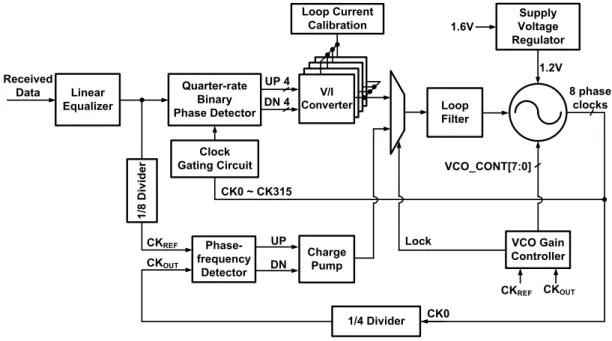
Fig. 2 shows a block diagram of the proposed CDR circuit with the adaptive loop bandwidth calibration and the idle power saved frequency acquisition. The CDR circuit consists of two loops which are a frequency acquisition loop and a phase tracking loop. Prior to the phase tracking operation, the frequency acquisition loop operates to lock clock frequency to input data rate using a training pattern of input data stream that is the 101010 toggle pattern. After the frequency acquisition, the phase tracking loop controls the trained clock in order to synchronize the clock phase with input data transitions using a quarter-rate binary phase detector and a V/I converter which generate a control signal of the VCO. Since the proposed CDR circuit uses the binary phase detector, design methods of the CDR loop parameters are different as compared with linear CDR circuit design which is based on a PLL circuit model [5]. As mentioned in Section I, jitter tolerance and jitter transfer function are representative jitter characteristics of the CDR circuit and the most important features. The -3-dB frequency of the jitter transfer (ω-3dB) and corner frequencies of the
jitter tolerance (ωc1, ωc2) can be defined as below [6]
-3 2 VCO p p dB m K I R p w f = (1) Quarter-rate Binary Phase Detector Received Data Linear Equalizer UP 4
DN 4 ConverterV/I Loop Filter Supply Voltage Regulator 1.6V 1.2V Loop Current Calibration 8 phase clocks Charge Pump UP DN Phase-frequency Detector CKREF CKOUT CK0 CK0 ~ CK315 1/4 Divider 1 /8 D iv id e r VCO Gain Controller CKREF CKOUT VCO_CONT[7:0] Lock Clock Gating Circuit
1 0.63 c p p R C p w = (2) 2 2 VCO p p c K I R w = (3)
where KVCO is the VCO gain (Hz/volt), Ip is the V/I
converter current, Rp, Cp are resistance and capacitance
of the loop filter, and Φm is the maximum phase change
by a single update of the bang-bang phase detector. From (1) ~ (3), it is noticed that the jitter characteristics are related to VCO gain, V/I converter current, and filter coefficients. However, the VCO gain and V/I converter current are sensitive to PVT variations. The variations of these parameters change the loop bandwidth of the CDR circuit, that is, jitter tracking and filtering abilities are changed from designed values, which increases BER of the CDR circuit.
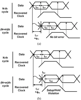
Fig. 3 shows a timing diagram of CDR operations. In case of the normal CDR operation, the clock signal recovered by the CDR circuit tracks input data jitter (tJIT).
This jitter tracking operation maintains setup time (tS)
and hold time (tH) between input data and the recovered
clock, which reduces BER. However, if KVCO and IP are
reduced by the PVT variations, ω-3dB and ωc2 become to
decrease and so the recovered clock is unable to track input data jitter, which increases BER. On the contrary, if
KVCO and IP are increased by PVT variations, the
increased open-loop gain of the CDR decreases phase margin and so the CDR circuit becomes instable [7]. Therefore, the VCO gain and V/I converter current should be robust to PVT variations in order to maintain jitter characteristics and avoid the increase of BER.
III. CIRCUIT DESCRIPTION
1. Current Calibration of V/I ConverterFig. 4 shows a block diagram of the current calibration circuit. This circuit consists of a V/I converter, a replica resistor multiplied by m, a bandgap reference, and a comparator. Initial VBIAS is supplied to the V/I converter
and output current of the replica V/I converter (Irp) flows
to the replica resistor (Rrp). The replica V/I converter
current and the resistor become VCAL and the comparator
compares the difference between VCAL and the output
voltage of bandgap reference (VBGR). VBGR is less
sensitive to PVT variations as compared with VCAL that is
changed by Irp variation. The comparison result is
applied to VBIAS value and the negative feedback loop
controls VBIAS until VCAL is equal to VBGR. If Irp variation
occurs due to PVT variations, the feedback loop minimizes Irp variation by eliminating the error between
(a)
(b)
Fig. 3. (a) Correct operation of a CDR circuit tracking input
data jitter, (b) setup/hold violation of a CDR circuit due to PVT variations. V/I Converter Replica V/I Converter Irp VBIAS Rp Cp Ip = 4xIv/i Rrp VBGR Band-gap Reference VCAL VCO Control Voltage Quarter-rate Binary Phase Detector 4 4
VCAL and VBGR. Therefore, in steady state, the replica V/I
converter outputs the variation-compensated current. Since Irp should continuously flow to the replica
resistor in order to maintain VCAL level steadily, the
replica resistor should be larger than Rp to reduce DC
power consumption. So, the coefficient of the replica resistor (m) can be defined as
BGR p V m I R = (4)
In this design, VBGR of 600-mV, Ip of 85-μA and R of
500-Ω are used. According to (4), m becomes 14 so that the replica resistor of 7-kΩ has been implemented.
2. Trimmable Bandgap Reference
Since VBGR is used as the reference point in the current
calibration, the bandgap reference should be robust to PVT variations. Fig. 5 shows a schematic of the bandgap reference. After the bandgap reference has started up by
VBGON, the main circuit generates a temperature-stable
current (Ic) that is composed of VD1/(R1C+R1D) and (VD1 -VD2)/RCAL1 which are complementary to absolute
temperature (CTAT) current and proportional to absolute temperature (PTAT) current, respectively. As the bandgap reference combines the CTAT and PTAT currents in order to eliminate temperature instability, the bandgap reference can generate the output voltage with temperature stability which is expressed as
2 1 1 1 1 ln CAL BGR D T CAL R R V V N V R R é æ ö ù = ê +ç ÷ ú ê è ø ú ë û
(5)
where VT is the thermal voltage, VD1 is the diode voltage,
and N is the area ratio between PNP BJTs. VTlnN is
equal to VD1-VD2 that is the PTAT component and R1 is
equal to R1A+R1B and R1C + R1D. The bandgap reference
has two error sources for the output voltage; 1) temperature characteristic mismatch between VD and VT
and 2) absolute output voltage offset. In this design,
RCAL1 and RCAL2 are implemented in order to calibrate
these unexpected offsets. Similar to the conventional bandgap references [8, 9], the temperature characteristic mismatch between VD and VT can be trimmed using
RCAL1. In addition, RCAL2 enables to calibrate the absolute
output voltage offset which causes Ip offset.
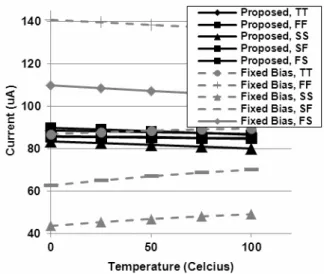
The post-layout simulation results of the proposed scheme are shown in Fig. 6. For 5 process corners with temperature sweep from 0°C to 100°C, the adaptive calibration scheme reduces Ip variation from 94.1-μA to
6.42-μA which is just 7% of the conventional current variation. Fig. 7 shows the post-layout simulation results of clock jitter for typical, fast, and slow corner variations. The simulation environment includes the data-dependent input jitter due to channel loss and the supply noise due to a chip power delivery network. The conventional circuit has 66-ps jitter variation between fast and slow corner processes. In case of the slow corner, since the loop bandwidth is reduced due to KVCO and IP reductions,
the clock phase change updated by the phase detector is
Fig. 5. Schematic of the digitally trimmable bandgap reference. Fig. 6. Simulated V/I converter current with and without the
relatively small. In case of the fast corner, the clock phase change becomes larger due to the increased loop bandwidth. However, in the proposed circuit, since the calibration scheme compensates temperature and process variations, the proposed circuit shows the maximum 5-ps of jitter variation between typical and slow corner processes.
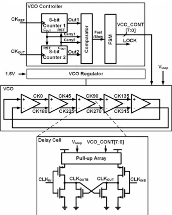
3. PVT Tolerant VCO with a Gain Calibration
Fig. 8 shows a schematic of the VCO block. In order to minimize the loop bandwidth variation caused by VCO gain variation, an exclusive power regulator and a VCO gain calibration circuit are implemented for the VCO which has PVT tolerant characteristics [10]. The regulator isolates the VCO supply voltage from noise sources which are generated by the other digital blocks. A 1.6-V supply is additionally used to generate the 1.2-V regulated supply voltage without a dropout voltage. Against temperature and process variations, the VCO gain calibration circuit finds proper digital codes for the VCO to operate within linear region where VDD/2 is
applied.
In the training mode, the received data toggles like a 2.7-GHz clock signal for 5.4-Gb/s operation. The received data and the VCO clock are divided and compared by 8-bit counters and a digital comparator. Two 8-bit counters count the number of cycles of the divided data (CKREF) and the divided VCO clock
(CKOUT) until one of them overflows. When a faster
signal between CKREF and CKOUT has finished the 8-bit
counting, the comparator compares the count numbers to
calculate clock frequencies of CKREF and CKOUT and
outputs decision signals, Fast and Slow. The finite-state machine uses Fast and Slow signals from the comparator to generate digital control bits, VCO_CONT[7:0]. These control bits are connected to pull-up arrays of the VCO delay cells. The pull-up array of the delay cell consists of PMOS transistors in parallel which are controlled by a loop filter voltage (Vloop) and VCO_CONT[7:0].
VCO_CONT[7:0] tunes the VCO coarsely in order to minimize the VCO gain variation for all process cases.
Fig. 7. Post-layout simulation results of the recovered clock
jitter.
Fig. 8. Block diagram and schematics of the VCO and its gain
controller.
Fig. 9. Post-layout simulation results of the VCO output
Fig. 9 shows simulation results of the calibrated VCO output using proper control codes for process and temperature variations. Each line represents the calibrated VCO output in different process and temperature conditions. In case of fast/fast process corner and 100°C condition, the gain calibration circuit generates the minimum value of VCO_CONT[7:0]. In contrast, in case of slow/slow process corner and -40°C condition, VCO_CONT[7:0] has the maximum value to increase the VCO gain and the oscillation frequency.
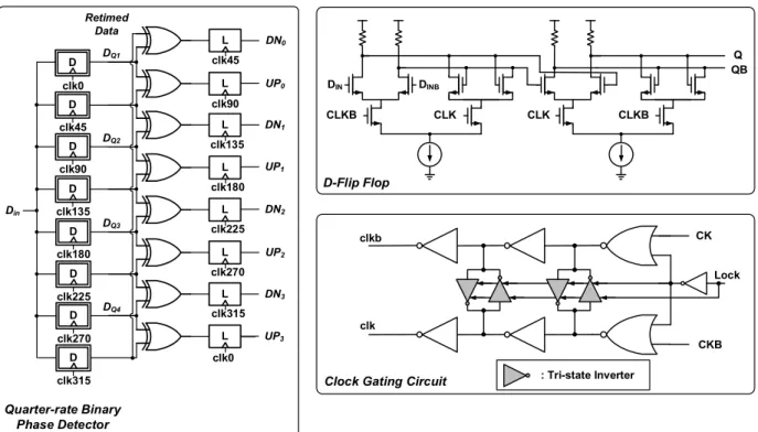
4. Quarter-rate Binary Phase Detector
A schematic of the quarter-rate binary phase detector is shown in Fig. 10. The phase detector is composed of 8 D-flip flops, 8 XOR gates, and 8 latches, which are current-mode logics for high-speed operation. 8-phase clock signals are connected to D-flip flops for data aligning and sampling. As the CDR circuit controls the recovered clock phase in the phase tracking mode, 0°-, 90°-, 180°-, and 270°-clock signals sample the received data at the middle and 45°-, 135°-, 225°-, and 315°-clock signals are aligned with the edges of the received data in order to find data transition points.
Before the phase tracking mode, in the frequency
acquisition mode, the CDR circuit operates like a PLL to match the clock frequency up with the data rate. In this mode, the phase detector does not work, but consumes the steady current from VDD to GND since a current mode logic always flows the steady current from VDD to GND even if the logic is idle. Nevertheless, the phase detector has to use current-mode logics inevitably because it is hard for CMOS logic circuits to handle the high-speed data over giga bit per second.
In the proposed circuit, to prevent the unnecessary power consumption, a clock gating circuit has been implemented for the phase detector. The clock gating circuit consists of NOR gates, inverters, and tri-state inverters. When Lock signal is low, the CDR operation mode is frequency acquisition and so the clock gating circuit outputs low for both clk and clkb as shown in Table 1. Therefore, input NMOS transistors of D-flip flops and latches are turned off and the current path between VDD and GND is also cut off.
In the phase tracking mode of the CDR circuit, Lock signal becomes high and the clock gating circuit supplies 8-phase clock signals to D-flip flops and latches in the phase detector in order to sample and deserialize the received data. As shown in the schematic of the phase detector, XOR gates are not clocked logics and so does
D clk0 clk45 clk90 clk135 clk180 clk225 clk270 clk315 DQ1 DQ2 DQ3 DQ4 L clk45 L clk90 L clk135 L clk180 L clk225 L clk270 L clk315 L clk0 DN0 UP0 DN1 UP1 DN2 UP2 DN3 UP3 Din D D D D D D D Retimed Data Quarter-rate Binary Phase Detector CLKB CLK DIN DINB CLK CLKB Q QB D-Flip Flop CK CKB clkb clk Lock
Clock Gating Circuit : Tri-state Inverter
not use any current blocking scheme, which means XOR gates always flow the steady current. Naturally, when the phase detector idles, it is possible to block the current flowing of XOR gates as pulling down the bias voltage to the ground level. However, if the steady current of the XOR is blocked, the outputs of XOR gates or the inputs of latches becomes high. In this case, when the CDR loop turns to the phase tracking mode, clock signals start to toggle and so the latches sample and propagate the high level outputs of XOR gates to 4 V/I converters. Since the outputs of latches are used as up and down signals of the V/I converters, the propagated high level signals generate V/I converter currents, which additionally consume the power and unnecessarily pull up the loop voltage. Therefore, as unblocking the steady currents of XOR gates, the outputs of XOR gates stay low and so the unwanted up pulse is not generated when clock signals start to toggle. Even though XOR gate currents are not blocked, the idle power consumption of the phase detector has been reduced from 10.89-mW to 2.4-mW with 1.2 V supply; 77.96% reduction in idle power consumption has been accomplished.
IV. MEASUREMENT RESULTS
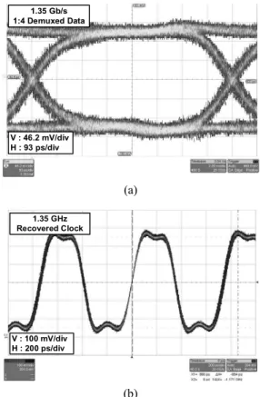
Fig. 11 shows the recovered data and clock of the CDR circuit with the adaptive loop bandwidth calibration. From 5.4-Gb/s PRBS-31 data, the CDR circuit recovers 4-phase 1.35-GHz clocks and 1:4 demuxed 1.35-Gb/s data. These data are transferred to a 4:1 mux and serialized to 5.4-Gb/s data for BER test. The proposed CDR circuit recovers data and clock with peak to peak jitter of 31.5 ps and rms jitter of 3.4 ps with the BER of < 10-12. In order to verify the adaptive loop calibration
scheme, jitter tolerances have been measured as the
Table 1. Power consumption of the quarter-rate binary phase
detector
Operation mode : Frequency acquisition
Data 1010 clock pattern
Lock signal Low
Inputs of clock gating circuit CLK, CLKB Outputs of clock gating circuit GND, GND 10.89 mW w/o clock gating Power consumption of the quarter-rate
binary phase detector
(8 D-FFs. 8 XORs, 8 latches) 2.4 mW with clock gating
1.35 Gb/s 1:4 Demuxed Data V : 46.2 mV/div H : 93 ps/div (a) V : 100 mV/div H : 200 ps/div 1.35 GHz Recovered Clock (b)
Fig. 11. (a) Measured data, (b) the recovered clock signal of the
CDR circuit. 0.1 1 10 100 1000
1.E+01 1.E+02 1.E+03 1.E+04 1.E+05 1.E+06 1.E+07 1.E+08
J it te r T o le ra n c e ( U Ip p ) Jitter Frequency (Hz) 60°C 100°C 24°C
Equipment Limit (MP1800A)
(a) 0.1 1 10 100 1000
1.E+01 1.E+02 1.E+03 1.E+04 1.E+05 1.E+06 1.E+07 1.E+08
J it te r T o le ra n c e ( U Ip p ) Jitter Frequency (Hz) 60°C 100°C 24°C
Equipment Limit (MP1800A)
(b)
Fig. 12. Measured jitter tolerance graph of the CDR circuits
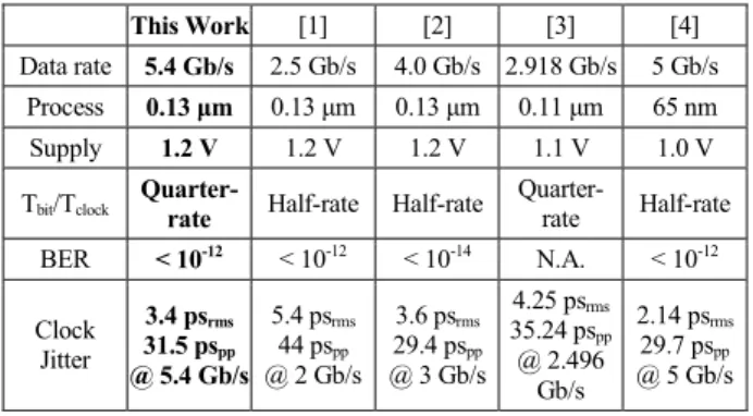
calibration circuit is turned on and off as shown in Fig. 12. At high temperature of 100°C, the jitter tolerance of the conventional scheme is decreased as compared with the measured result at 24°C, but the proposed scheme shows similar jitter tolerances as compared with the same measurement at 24°C. For 1-MHz input jitter, the proposed scheme shows the jitter tolerance of 0.45-UI which is 0.25-UI larger as compared with the conventional scheme. Total 19 samples have been measured and shown the same differences between calibration-on/off experiment results. Fig. 13 shows a die photograph of the proposed CDR circuit. The test chip has been fabricated using 0.13-μm CMOS technology and the calibration circuit consumes 0.096 mm2. Table 2 shows the summary and comparisons with the previous works. The measured power dissipation is 105-mW including output drivers and an embedded 4:1 MUX at 5.4-Gb/s data rate.
V. CONCLUSIONS
This paper introduces a clock and data recovery circuit that adaptively calibrates the loop bandwidth and
minimizes the idle power consumption of the quarter-rate phase detector and V/I converters in the frequency acquisition mode. Since the loop bandwidth of the CDR circuit is proportional to V/I converter current and VCO gain, the loop bandwidth calibration consists of the adaptive loop current calibration circuit with the proposed trimmable bandgap reference circuit and the VCO gain controller for the VCO operation in the linear control region. The quarter-rate phase detector accomplishes high bandwidth and low stand-by current consumption using a clock gating circuit which reduces 77.96% of the idle power consumption by the phase detector. In the experiment, the proposed scheme reduces the jitter tolerance variation from 0.45-UI to 0.2-UI at 1-MHz as compared with the conventional circuit. The chip has been fabricated in a 0.13-μm CMOS technology. The measured power dissipation with 1.2-V supply is 105-mW including output drivers and an embedded 4:1 MUX at 5.4-Gb/s data rate.
ACKNOWLEDGMENTS
This research was supported by the MSIP(Ministry of Science, ICT and Future Planning), Korea, under the ITRC(Information Technology Research Center) support program(IITP-2017-2016-0-00311) supervised by the IITP(Institute for Information & communications Technology Promotion).
REFERENCES
[1] R. Inti et al., “A 0.5-to-2.5Gb/s reference-less half-rate digital CDR with unlimited frequency acquisition range and improved input duty-cycle error tolerance,” IEEE J. Solid-State Circuits, vol. 46, no. 12, pp. 3150-3162, Dec. 2011.
[2] H. Song et al., “A 1.0-4.0-Gb/s all-digital CDR with 1.0-ps period resolution DCO and adaptive proportional gain control,” IEEE J. Solid-State
Circuits, vol. 46, no. 2, pp. 424-434, Feb. 2011.
[3] S. Kim et al., “A 1.248 Gb/s – 2.918 Gb/s low-power receiver for MIPI-DigRF M-PHY with a fast settling fully digital frequency detection Loop in 0.11 μm CMOS,” IEIE J. Semiconductor
Technology and Science, vol. 15, no. 4, pp.
506-517, Aug. 2015.
Fig. 13. Die photograph.
Table 2. Performance Summary and Comparison
This Work [1] [2] [3] [4]
Data rate 5.4 Gb/s 2.5 Gb/s 4.0 Gb/s 2.918 Gb/s 5 Gb/s Process 0.13 μm 0.13 μm 0.13 μm 0.11 μm 65 nm Supply 1.2 V 1.2 V 1.2 V 1.1 V 1.0 V Tbit/Tclock
Quarter-rate Half-rate Half-rate
Quarter- rate Half-rate BER < 10-12 < 10-12 < 10-14 N.A. < 10-12 Clock Jitter 3.4 psrms 31.5 pspp @ 5.4 Gb/s 5.4 psrms 44 pspp @ 2 Gb/s 3.6 psrms 29.4 pspp @ 3 Gb/s 4.25 psrms 35.24 pspp @ 2.496 Gb/s 2.14 psrms 29.7 pspp @ 5 Gb/s
[4] T. Lee, Y.-H. Kim, J. Sim, J.-S. Park, and L.-S. Kim, “A 5-Gb/s 2.67-mW/Gb/s digital clock and data recovery with hybrid dithering using a time-dithered delta–sigma modulator,” IEEE Trans.
Very Large Scale Integration (VLSI) Systems, vol.
24, no. 4, pp. 1450-1459, Apr. 2016.
[5] S. Byun et al., “A 10-Gb/s CMOS CDR and DEMUX with IC a quarter-rate linear phase detector,” IEEE J. Solid-State Circuits, vol. 41, no. 11, pp. 2566-2576, Nov. 2006.
[6] J. Lee, K. S. Kundert, and B. Razavi, “Analysis and modeling of bang-bang clock and data recovery circuits,” IEEE J. Solid-State Circuits, vol. 39, no. 9, pp. 1571-1580, Sep. 2004.
[7] B. Razavi, Design of integrated circuits for optical communications, 1st ed., McGraw-Hill, 2003, pp. 318-322.
[8] K. N. Leung, and Philip K. T. Mok, “A Sub-1-V 15-ppm/°C CMOS Bandgap Voltage Reference Without Requiring Low Threshold Voltage Device,” IEEE J. Solid-State Circuits, vol. 37, no. 4, pp. 526-530, Apr. 2002.
[9] H. Abbasizadeh et al., “Accurate sub-1 V CMOS bandgap voltage reference with PSRR of -118 dB,”
IEIE J. Semiconductor Technology and Science,
vol. 16, no. 4, pp. 528-533, Aug. 2016.
[10] H. I. Lee et al., “A ΔΣ fractional-N frequency synthesizer using a wideband integrated VCO and a fast AFC technique for GSM/GPRS/WCDMA applications,” IEEE J. Solid-State Circuits, vol. 39, no. 7, pp. 1164-1169, Jul. 2004.
Won Young Lee received the B.S., M.S., and Ph.D. degrees in Electrical Engineering from Korea Advanced Institute of Science and Technology (KAIST), Daejeon, Korea, in 2006, 2008, and 2012 respectively. From 2012 to 2015, he was a senior engineer at Samsung Electronics, Korea. In 2015, he joined the faculty of Electronic IT Media Engineering at Seoul National University of Science and Technology, Korea, where he is currently an assistant professor. His research interests include PLL, CDR, and equalizer designs for high-speed interfaces.
Chae Young Jung was born in Gunsan, Korea. She is currently an undergraduate student in the Department of Electronic IT Media Engineering at Seoul National University of Science and Technology. Her research interests include low power clocking circuit design.
Ara Cho was born in Daegu, Korea. She is currently an undergraduate student at Seoul National University of Science and Technology and majoring in Electronic IT Media Engineering. Her research interests include high-speed CMOS interface circuit design and jitter tracking circuits.