• Wafer-Level Processes - Metallic Thin Film
- Thin-Film Deposition
Physical Vapor Deposition
Resistive Evaporation
Electron-Beam Evaporation Sputter Deposition
Chemical Vapor Deposition LPCVD
PECVD
Lecture 5
Microfabrication
– Wafer-Level Processes (III)
- Usage
Conductors Resistors
Mechanical elements Transducer elements - Deposition techniques
(1) Resistive evaporation
(2) Electron-beam evaporation (3) Sputter deposition
(4) Magnetron sputter deposition (5) CVD
(6) Laser-assisted CVD (7) Electrodeposition
Metallic Thin Film
- 잘 녹지 않는 metal “boat”를 사용.
- 10-3 ~ 10-2 Torr까지의 vapor pressure를 만드는 온도까지 상승시킬 수 있는 금속은 가능.
- 승화하기도 하므로 용융점이 중요한 것은 아님.
- Tungsten boat가 1400 ºC까지 쓸 수 있으므로 Au, Al, Mg 등은 적절하고, Cr은 경계에 있다.
- Vapor condensation process. 금속 원자는 표면에 도착하면 붙어 버린다. 이것은 step coverage나 stress를 좋게 하는 움직임을 없게 한다.
- 기판 온도는 stress에 영향을 주어 가열하지 않은 기판은 일반적으로 tensile이다.
- 저 융점 금속(Al, Au)는 stress가 낮으나, 융점이 높은 금속일수록 stress가 커진다.
- Sputter한 막보다 접착력이 나쁘고 대개 0.5 ~ 5 nm/s 정도의 증착율을 보인다.
Resistive Evaporation
- Electron beam (8~10 keV, generally 100~200 mA)이 target을 scan해서 vapor를 만든다.
- Electron beam power, 초점, target 냉각 등에 의해 조절되고 온도는 2800 ºC까지 올라간다.
- Resistive evaporation으로 가능한 금속, Ti, Pt, Pd, 녹기 어려운 W, Mo, Ta도 가능하다.
- W는 실리콘과 선열팽창계수가 비슷해 유용하다.
- CVD나 sputtering (5~200 nm/s)보 다 빠 른 증 착 이 가 능 하 고, resistive evaporation보다는 기판 온도가 낮다.
- Metal 과 Dielectric도 가능하나 같은 기계를 쓰지는 않는다.
Electron-Beam Evaporation
(continued)
- 가열하지 않는 기판에서는 일반적으로 tensile이고 고 융점 금속일수록 stress가 올라간다.
- Al이나 Mg 같은 “soft material”로부터 발생하는 x-ray는 100~200 eV이다.
Target 아래에 있는 Cu (열전도를 위한 것)에 beam이 맞아서 K-α x-ray가 발생하지 않는다면 이 정도는 인체에 해를 주지 않는다.
- 그런데 K-α x-ray는 30 kV 가속 전압이 필요하고, 대부분의 electron-beam evaporator는 10 kV 이하이다.
- Ion gun은 film을 compressive로 만든다. Gun으로부터의 에너지와 ion flux를 조절하면 그 양을 조절할 수 있고 고 융점이나 high tensile stress film에 대해서는 ion gun을 보조로 사용하면 stress를 적게 할 수 있다.
- 표면을 때린 ion이 extra energy를 금속 원자에 주어서 좀 더 조밀하게 (compact) 정렬시켜 compressive가 된다.
Electron-Beam Evaporation
- 불활성 기체의 이온 (예를 들면, Ar+ )이 DC나 RF 구동에 의해 가속되어서 target을 때리고 그 momentum에 의해 target 물질이 튀어 나온다.
- 충분히 높은 에너지의 플라즈마가 발생한다면 거의 대부분의 물질을 sputter할 수 있다 (단, dielectric은 RF sputter가 필요하다).
- Methods to obtain plasma.
(1) DC glow discharge - 장치가 간단하고 soft material만이 가능하며 low energy plasma 만을 발생.
(2) Planar RF - 전극 판 두개가 평행 위치, target에 RF를 가함. Dielectric도 가능.
(3) Planar magnetron - 자기장이 반원의 전자 궤도를 만들고, 가스 분자와의 상호작용을 증가 시켜 더 많은 이온을 만든다.
(4) Cylindrical magnetron or S-gun - 전자를 위해서 자기적으로 “race- track”과
같은 폐 회로를 만들고 기판으로부터는 멀리 떨어뜨리고 target 근처에 high-energy plasma를 만든다.
Sputter Deposition
(continued)
- Sputtering은 evaporation 보다 원자에 에 너지를 많이 주어서 surface mobility가 크고 resputtering이 되기도 한다. 따라서, step coverage가 좋고 stress control이 좋다. 역으로 lift-off가 어렵다.
- Sputtering으로 alloy나 dielectric compound를 올릴 수 있다 (TiNi, PZT, NdTbFeB 등).
- Sputter로 형성된 막은 tensile이고 심하면 yield strength를 넘기도 한다. Cr, Ti, Ni, Mo, Ta 등은 낮은 기압에서는 compressive가 된다.
Stress가 바뀌는 압력은 무거운 원자의 금속일수록 증가한다.
Illustration of relationship among pressure, atomic mass of the metal, and stress in sputtered films.
Sputter Deposition
- Step coverage
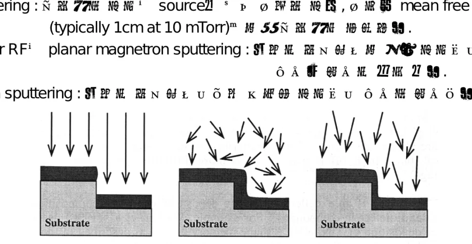
Evaporation : source로부터 방향성을 갖는다. 그래서 step coverage가 나쁘다. Lift-off에는 유리.
Sputtering : 방향성은 있으나 source가 널리 분포해 있고, 분자는 mean free path (typically 1cm at 10 mTorr)내에서 방향성을 유지한다.
Planar RF나 planar magnetron sputtering : 기판이 플라즈마에 담겨 있으므로 벽면과 표면이 거의 같다.
S-gun sputtering : 기판이 플라즈마로부터 떨어져 있으므로 벽면은 표면보다 얇다.
Illustration highlighting the differences in step coverage between evaporation (left), planar sputtering (center), and S-gun sputtering (right).
Comparison of Evaporation and Sputtering
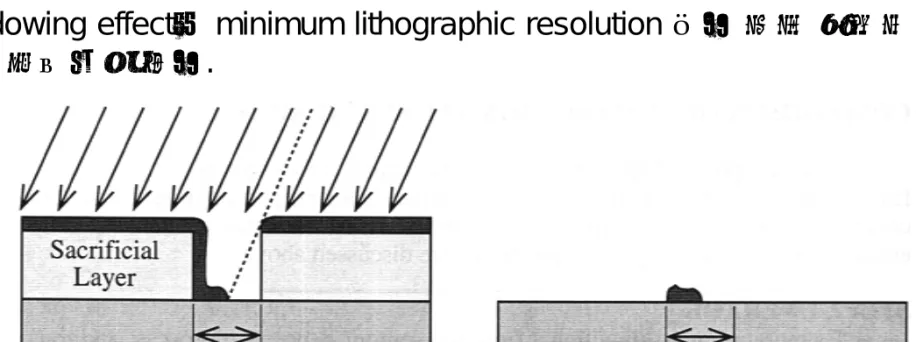
- Shadow effect는 문제를 일으키기는 하나 마이크로머시닝에서는 유용하기도 한다.
- Step coverage를 좋게 하기 위해서 웨이퍼를 돌리면서 증착하기도 한다.
- Shadowing effect는 minimum lithographic resolution 보다 작은 선폭을 만드는 데 이용되기도 한다.
Illustration of the use of shadowing to produce features finer than the lithographic resolution. At left, a sacrificial layer (typically photoresist) is used to deposit metal at a known angle. At right, after removal of the sacrificial layer, a finer structure remains than the original line width. This approach is similar to standard “lift-off” deposition (discussed below), but in that case, an overhanging “lip” of photoresist is used to aid removal of the unwanted metal.
Shadowing
mirror plate
address electrode vertical spring
a’
a
Va
S
Va S
(a) undeflected state
(b) deflected state
A schematic illustration of micromirror with vertical spring.
- J. W. Shin : Sensors and Actuators, Vol.A66, 144-149,1998
Vertical Spring for Micromirror
(a) electrode definition
(b) sacrificial layer definition
(c) spring evaporation
with some incident angle (shadow evaporation)
(d) fill up holes
(e) mirror evaporation
(f) sacrificial layer removal
silicon
oxide
aluminum
thick PR
Fabrication process sequence of micromirror array with vertical spring.
Fabrication Process
(a) SEM photograph of fabricated micromirror array (side-view)
(b) magnified view of micromirror array in (a)
Micro Mirror Array
vertical spring
Fabricated vertical spring array.
Chemical Vapor Deposition
• A class of deposition methods in which precursor materials are introduced into a heated furnace.
• A chemical reaction occurs on the surface of the wafer, resulting in deposition.
• Silicon films are formed from the decomposition of silane (SiH4), with hydrogen as a gaseous byproducts.
• Silicon nitride is formed by the reaction of dichlorosilane (SiH2Cl2) and ammonia (NH3), with hydrogen and HCl vapor as gaseous byproducts.
• Silicon dioxide is formed by the reaction of silane or silane derivative with a suitable oxidizing species.
• CVD depositions are typically performed under low-pressure conditions (less than 1 mTorr) and usually involve an inert diluent gas, such as nitrogen, in addition to the reacting species.
LPCVD and Metallization
• Low pressure CVD, most commercially important.
• With the exception of silicon, CVD processed typically involve temperatures in the range of 500o to 850oC.
• These temperatures are too high to perform on wafers that have been metallized with either aluminum or gold, which form eutectics with silicon at 577oC and 380oC, respectively.
• It is necessary to perform all CVD processes before any depositions with these metals.
• Tungsten is able to withstand CVD temperatures.
Epitaxy
• If CVD deposition occurs on a single-crystal substrate, it is possible for the underlying crystal to serve as a template for the deposited material to develop as an extension of the single crystal.
• Epitaxy is used for silicon and also for various III-V compounds, such as GaAs.
• Taking the case of silicon as an example, there is a relation between substrate temperature, deposition rate, and crystal growth.
• If at given temperature, the deposition rate is slow enough to provide ample time for atoms to migrate along the surface and find equilibrium lattice sites, then epitaxy is possible.
• At higher deposition rates, the deposition occurs as polysilicon.
(continued)
Epitaxy
• In Figure, it is seen that the maximum deposition rates, the deposition rates for epitaxy drop dramatically with temperature.
• One interesting feature of silicon epitaxy is that if a portion of the single- crystal wafer is exposed, while the rest is covered with silicon dioxide, epitaxial growth can occur over the single-crystal regions while polysilicon is being deposited over the oxide.
The relation between deposition rate, temperature, and the morphology of the deposited CVD silicon film.
PECVD
• Plasma-Enhanced CVD
• Deposition rates can be enhanced if the deposition occurs in a glow- discharge plasma.
• PECVD is used to deposit dielectric films at lower temperature (below 400oC) that could be achieved without the plasma assist.
• This is extremely important in constructing insulation layers for use with metallization.
Film and Process
• Films deposited by LPCVD are either amorphous, in the case of the inorganic dielectrics, or polycrystalline, in the case of polysilicon or metals
• The material properties can depend in detail on the exact process, including such issues as temperature, gas flow rates, pressures, and the chemistry or morphology of the layer on which the film is deposited.
• The mass density of a deposited film, for example, depends on how many voids are present (regions where atoms could fit, but, because of the relatively low temperature of deposition, do not get filled up).
• Thermally grown silicon dioxide has fewer voids than LPCVD silicon dioxide, which, in turns, has fewer voids than lower-temperature PECVD silicon dioxide.
• In addition, the CVD oxides have some residual hydrogen.
• Post-deposition anneals are used to densify the films
- 원하는 금속 원자가 실리콘 원자와 치환하는 반응으로 금속 막을 얻는다. - Tungsten은 low-pressure CVD로 선택적인 증착이 가능하다.
- SiO2를 mask로 사용하고 WF6 gas를 silicon이나 polysilicon에 쏘여 주면 된다.
- Busta : 텅스텐으로 filament, loop, pyramid, field emitter structure 등을 제작 했다.
- Mac Donald : 텅스텐으로 honeycomb, harmonic motor 등을 제작했다. - Manginell : platinum을 선택적으로 증착, 산소 내의 수소를 알아내는
가스센서로 사용.
4
6
3 2 3
2 WF + Si → W + SiF
Selective Metal CVD
SEM top view of a pair of filaments. Al bond wires connect the square bond pads to a conventional dual in-line package (DIP). Only the lower filament which was electrically heated in the CVD cell contains a 0.2 µm layer of Pt.
The micro-CVD apparatus: A teflon “CVD cell” houses the packaged filament and a small amount of the Pt precursor. The cell is equipped with electrical access to provide power to those filament selected for deposition.
Nitrogen lines insure an inert ambient in the cell. To vaporize the precursor, the CVD cell is inserted in to an oven at 140 ºC.
- R. P. Manginell, Solid-State Sensor and Actuator Workshop, pp.23-27, 1996.
- Pt precursor (platinum acetylacetonate)를 140 ºC의 CVD에 넣고 filament를 넣는다.
- Pt는 450 ºC를 넘어야 filament에 형성된다. - 단자에 전류를 흘려 filament를 가열.
- 전류를 dc로 흘리거나 20 Hz의 pulse를 duty cycle을 바꿔 가면서 가열.
Selective CVD of platinum
Near-profile SEMs of the ends of two filaments subjected to different deposition conditions.
The high surface-area film on the top filament was deposited in continuous mode for 10 minutes. The lower film underwent a 9 % duty- cycle (5 msec on, 50 msec off) deposition for a total elapsed time of 7 min., and is relatively smooth in comparison to the upper film.
- 10분간 전류를 계속 흘린 경우 표면이 상당히 거칠어짐.
- 이 것 은 catalyst precursor 의 mass- transport가 제한되기 때문이다.
- Duty-cycle이 클수록 거칠어짐.
- 9 % duty-cycle의 경우 film이 고움.
Results
- 접착력이 좋지 못한 non-reactive metal 아래에 Ti, Hf (Hafnium, 융점 2230 ºC), Cr 등의 reactive metal을 adhesion layer로 10~30 nm 정도 형성한다.
- 금, 백금과 다른 low-reactivity metals 등에는 절대적으로 필수적이다.
- 보통 Ti/Au/Ti의 3층 막을 사용. Ti 30nm/Au 500 nm/Ti 30 nm.
- 전기적으로 연결한다면 위의 티타늄은 제거해야 한다.
- Adhesion metal은 증착할 금속과 합금을 만들 수도 있으므로 Pt 또는 Pd와 같은 확산 방지 층을 삽입해야 한다.
- 금은 티타늄을 통해서 GaAs나 Silicon 기판으로 확산할 수 있다.