저작자표시-비영리-변경금지 2.0 대한민국 이용자는 아래의 조건을 따르는 경우에 한하여 자유롭게 l 이 저작물을 복제, 배포, 전송, 전시, 공연 및 방송할 수 있습니다. 다음과 같은 조건을 따라야 합니다: l 귀하는, 이 저작물의 재이용이나 배포의 경우, 이 저작물에 적용된 이용허락조건 을 명확하게 나타내어야 합니다. l 저작권자로부터 별도의 허가를 받으면 이러한 조건들은 적용되지 않습니다. 저작권법에 따른 이용자의 권리는 위의 내용에 의하여 영향을 받지 않습니다. 이것은 이용허락규약(Legal Code)을 이해하기 쉽게 요약한 것입니다. Disclaimer 저작자표시. 귀하는 원저작자를 표시하여야 합니다. 비영리. 귀하는 이 저작물을 영리 목적으로 이용할 수 없습니다. 변경금지. 귀하는 이 저작물을 개작, 변형 또는 가공할 수 없습니다.
碩士學位論文
Deposit zinc oxide thin film at atmospheric pressure using
dielectric barrier discharge.
濟州大學校大學院
에너지工學科
무하마드 라기브 만수르
Deposit zinc oxide thin film at atmospheric pressure using
dielectric barrier discharge.
指導教授 李憲周
무하마드 라기브 만수르
이論文을工學碩士學位論文으로
提出
함2009 年 06 月
무하마드 라기브 만수르 工學碩士學位論文 을
認准
함審查委員長 印
委 員 印
委 員 印
濟州大學校大學院
2009 年 06 月
Deposit zinc oxide thin film at atmospheric pressure
using dielectric barrier discharge.
Muhammad Rakib Mansur
(Supervised by professor Heon-Ju Lee)
A thesis submitted in partial fulfillment of the requirement for the degree of Master of Science.
2009.06.
The thesis has been examined and approved
………. Thesis director
Professor Heon-Ju Lee, Nuclear and Energy Engineering
………. Professor Won Gee Chun, Nuclear and Energy Engineering
………. Professor Choi Chi Kyu, Department of Physics
……… Date
Department of Nuclear and Energy Engineering
ABBREVIATION
ZnO : Zinc Oxide
DBD : Dielectric barrier discharge OES : Optical Emission Spectroscopy XPS : X- Ray Photoelectron Spectroscopy
FESEM : Field Emission Scanning Electron Microscopy PECVD : Plasma Enhanced Chemical Vapor Deposition ARE : Activated Reactive evaporation
Dedicated to my
Teachers and all of my Family members
ACKNOWLEDGEMENT
I feel greatly indebted to my advisor professor Heon-Ju Lee for his support and guidance throughout my masters at Jeju National University. This work would not have been possible without his guidance, encouragement, helpful discussion and keen interest. He has helped me not only in studies but as a mentor. As a mechanical engineer I was not very familiar with the plasma technology at the beginning. It’s his full credit to give me the opportunity by selecting me as his student and open a new horizon of knowledge.
Lots of thanks and gratitude to Prof. Wong Gee Chun under whom I have taken three courses learned about different aspects of thermodynamics and renewable energy. The courses he taught with great care and intellect, blended theoretical knowledge with practical interest. I also thank Prof. Choi Chi Kyu as one of my thesis supervisor. Thanks go to him to give me the honor of being a student under his kind supervision and giving some his precious time.
I am also very much grateful to Dr. Oleksiy V. Penkov and Dr. Vadim Yu plaksin in many ways. Not only in this experiment but in many ways Dr. Oleksiy V. Penkov has given me guidance. My inquisitiveness regarding thin film deposition, chemical surface analysis and crystallography is mainly due to him. During my first semester in Jeju National Univesity I have done plasma diagnostic course under Dr. Vadim Yu Plaksin and started journey towards this difficult but interesting field. Discussion with him always gives me more insights.
In many ways I am indebted to my lab mates Ji Hun Kim, Min Gook Ko, Chan Ju Im, Sang Beom Joa, Kang Bong Suk, Kim Yu Young, Young Jun Lee for helping me. I will always remember their friendship. Especially I have to thank my senior lab mate Ji Hun Kim who is very much kind and helpful in all respect.
educated giving me all sorts of support from my birth. To my younger brother who is not only my younger brother but best likeminded friend who feels for me. To my loving wife whom I newly married gives my life to a new meaning and momentum.
I greatly honor the kind and generous assistance given by Korean Government under Brain Korea 21 (BK 21) project. I am very much proud, grateful and delighted to study in Jeju National University. I will always remember the unique picturesque landscape, healthy and friendly environment of the University and Jeju Island.
Overall I have to pay gratitude to God Almighty who has given me the opportunity and ability to study and perform experiment in search of knowledge.
CONTENTS
요약문 ……… 13
ABSTRACT ……… 14
1 INTRODUCTIN ……… 15
2 RELATED THEORY 2.1 Plasma and processing ……… 16
2.2 Evaporation process ……… 16
2.3 Gas discharge ……… 18
2.4 Corona spark and arc ……… 21
2.5 Low temperature non thermal plasma (Dielectric barrier discharge) ……… 21
2.6 Source of energy to release electron ……… 25
2.7 Reactions inside plasma ……… 26
2.8 Plasma Surface interaction ……… 28
2.9 Optical Emission ……… 29
3 EXPERIMENTAL DETAIL 3.1 Experimental configurations ……… 30
3.2 Parallel plate configuration ……… 30
3.3 Coaxial plate configuration ……… 32
3.4 Disk plate configuration ……… 33
3.5 Equipments used for the measurement ………… 34
4.1 Optical Emission Spectroscopy of non thermal plasma
……… 35
4.2 Surface analysis of deposited samples……… 37
4.3 Surface topography of deposited ZnO thin film……….. 38
4.4 Voltage and current characteristic ……… 39
4.5 Relation between Frequency and breakdown voltage... 40
4.6 Dependence of deposition thickness on electrode gap .. 42
5 SUMMARY AND CONCLUSION 5.1 Summary ……… 43
5.2 Conclusion ……… 43
5.3 Future work ……… 44
LIST OF FIGURES
Figure 2.3.1 Nonlinear current voltage characteristic of different types of discharges.
.... 19
Figure 2.3.2 Paschen curve for a simple tube-type DC discharge .... 20
Figure 2.3.3 Paschen curve for air in log–log scale. Temperature 20 °C. Calculated VB = 6.72√ (pd) + 24.4(pd) [7].
.... 20
Figure 2.5.1 Schematic illustration of the interplay of pulsed electrical energy, discharge physics occurring in the bulk gas, then plasma chemistry in the silent discharge.
.... 21
Figure 2.5.2 Charge and shape distribution of electron avalanche at time t1 & t2 at external field E.
.... 22
Figure 2.5.3 The life cycle of one filament. The electron current je generates the excited species A , which in turn reacts to form the product B. The time scale, τ, of the three processes are very different.
.... 23
Fig. 2.6.1 Electron potential energy when an external field is applied to the metal.
.... 25
Figure 2.7.1 Activation energy diagram for a thermally-driven (solid line) and for a plasma-enhanced (dashed line) reaction [7].
.... 28
Figure 2.8.1 Plasma surface interaction diagram. .... 29
Figure 3.2.1 Schematic diagram for parallel plate configuration. .... 31
Figure 3.2.2 Parallel plate experimental set up. .... 31
Figure 3.3.1 Schematic diagram for coaxial electrode configuration. .... 32
Figure 3.3.2 Experimental set up of the coaxial type DBD set up. .... 32
Figure 3.4.1 Schematic set up of disk plate configuration to deposit ZnO. .... 33
Figure 4.1.1 Emission spectrum of non thermal plasma at visible range at atmospheric condition.
.... 35
Figure 4.1.2 Emission spectrum of non thermal plasma at visible range while deposition (When gases are supplied).
.... 36
Figure 4.3.1 Surface of ZnO layer on silicon substrate at about 10000 times magnification.
.... 38
Figure 4.3.2 Cross sectional view of the deposited ZnO. .... 38
Figure 4.4.1 Voltage current relationship with time of Parallel plate DBD. .... 39
Figure 4.4.2 Voltage current relationship with time of Disk plate configuration.
.... 39
Figure 4.4.3 Voltage current relationship with time of Coaxial type DBD. .... 40
Figure 4.5.1 Relation between Frequency and Breakdown voltage in coaxial type configuration (gap between two electrodes is 4 mm).
.... 40
Figure 4.5.2 Relation between Frequency and Breakdown voltage in coaxial type configuration (gap between two electrodes is 5.5 mm).
.... 41
Figure 4.5.3 Relation between Frequency and Breakdown voltage in disk plate type configuration.
.... 41
LIST OF TABLES
Table 2.1 Influence of plasma on three steps of film deposition by ARE process.
.... 17
Table 2.2 Multiplication of electrons in an avalanche at p= 1 atm, in electric fields E and breakdown gap d [4].
.... 24
Table 2.3 Work function for typical elements [7] .... 24
Table 2.4 Mean free paths measured at 15°C and 760 Torr [7]. .... 26
요약문
Zinc oxide (ZnO)박막은 투명하고, 전기적으로 전도성을 가지고 있어 여러 산업에 폭넓게 응용되고 있다. 최근에는 화학기상증착법 (CVD; Chemical Vapor Deposition), PECVD (Plasma Enhanced CVD), 펄스 레이저 증착법 (Pulsed Laser Deposition), 이온 빔 스퍼터링, 마그네트론 스퍼터링, 스프레이 열분해 등 여러 기술들이 ZnO 박막 증 착을 위해 사용 되고 있다. 본 연구실에서는 대기압에서 ZnO 증착 등 여러 목적을 위해 직류 아크 플라즈마트론을 개발 하였다. 이번 연구의 목적은 유전체 장벽 방전 (DBD)을 이용하여 ZnO 박막을 증착하고, 이를 위해 동축형, 평판형, 디스크형의 3 가지의 DBD 장치를 개발하여 ZnO 증착 공정을 수행하였다. 플라즈마 증착 공정은 플라즈마의 물리화학적 작용, 전원의 주파수, 파워, 가스의 압력 및 조성, 유량, 주입 형태, 전극의 구조에 따라 달라진다. 전극의 구조가 non-thermal 플라즈마에 대하여 크게 영향을 미치기 때문에 본 연구에서는 ZnO 증착을 위해 전극의 모양, 간격, 구 조 등을 달리하여 실험하였다. 박막 위에 증착된 ZnO 박막의 조성을 알아보기 위해 엑스선광전자분광기(X-ray photoelectron spectroscopy)로 측정을 하였고, 증착된 박 막의 표면을 살펴보기 위하여 장방출 주사전자현미경(Field Emission Scanning Electron Microscope)으로 측정을 하였다. 증착에 영향을 미치는 플라즈마의 이온의 종류 등을 알아보기 위하여, OES (Optical Emission Spectroscopy)로 분광분석을 하였 다.
ABSTRACT
Zinc oxide (ZnO) is a widely applied material in industry and technically important due to its wide range of optical and electrical properties. Recent years different techniques have already been adopted to deposit it include chemical vapor deposition, plasma enhanced chemical vapor deposition (PECVD), pulsed laser deposition, ion beam sputtering, magnetron sputtering, spray pyrolysis etc. In our lab DC arc plasmatron [10] has been designed and used for several purposes including ZnO deposition at atmospheric condition. The main objective of my experiment is to use dielectric barrier discharge to excite the ZnO vapor and observe the deposition occurred on the silicon substrates. Three different dielectric barrier discharge configurations have been developed to achieve deposition. In the experiment deposition of ZnO thin films on Silicon wafer has been done by using coaxial, parallel plate and disk plate type dielectric barrier discharge at atmospheric pressure. The deposition process depends on physical and chemical interactions in the plasma, frequency, power, gas pressure & composition, the magnitude and the pattern of the gas flow and electrode geometry. As electrode geometry has great impact on non-thermal plasma the main objective of the experiment is to apply different electrode configurations with different gaps & electrode geometry and observe the impact on ZnO deposition. X-ray photoelectron spectroscopy (XPS) has been used to reveal the presence of ZnO on the substrate, FESEM for surface observation. Optical Emission spectroscopy has been used to determine different element & ion species present at the different environment which could affect the deposition.
Keywords: Dielectric barrier discharge, zinc oxide, silicon wafer, atmospheric pressure, silicon wafer, non-thermal plasma.
1
INTRODUCTION
Zinc oxide is a semiconductor with a wide band gap 3.3 eV has hexagonal wurzite structure [1]. It is a potential material for solar cells, liquid crystal flat panel displays, energy efficient windows, gas sensors, surface acoustic wave devices, piezoelectric devices, ultrasonic transducers and many more [1].
Dielectric barrier discharge at atmospheric pressure is already used as a tool to deposit versatile organic coatings at moderate power input [5]. The aim of the experiment is to see whether low temperature non thermal plasma created by dielectric electric barrier discharges are able to deposit ZnO on silicon substrates or not. Process like plasma enhanced chemical vapor deposition (PECVD) requires high vacuum which is power hungry and require complicated machineries. Other advantages of DBD are it consumes low electric power, do not produce much heat and have negligible problem with sputtering [2]
Dielectric barrier discharge at atmospheric pressure is already implemented to do etching & surface moderation of different materials. But the transient nature of dielectric barrier discharges at atmospheric pressure and dependence on so many variables like gas pressure, electrode material, electrode geometry & so on made it difficult to get controlled deposition using dielectric barrier discharge, theoretically & experimentally. From the experiment it is evident that it is possible to deposit ZnO on silicon substrates using dielectric barrier discharge as a tool. There is no deposition only using ZnO vapor but the plasma created by dielectric barrier discharge at atmospheric pressure started and enhanced the deposition. The process which we have used is similar to activated reactive evaporation of the precursor as we have used oxygen for the activation.
2
RELATED THEORY
2.1 Plasma and processing:
Plasma is a gas containing charged and neutral species, including some or all of the following: electrons, positive ions, negative ions, atoms, and molecules. On average plasma is electrically neutral, because any charge imbalance would result in electric fields that would tend to move the charges in such a way as to eliminate the imbalance. The increasing use of plasmas in deposition technology in the past few years is due to stringent requirements of low temperature processing in modern microelectronics and optoelectronic industries. Plasma is a convenient source of activated gas atoms and molecules, and energetic neutrals and ions, which can be used to overcome the activation energy barrier for a particular chemical reaction. That is why it becomes possible to synthesize a given compound in a plasma environment at relatively low substrate temperatures, compared to non-plasma, thermal process.
2.2 Evaporation process:
Evaporation processes for the deposition of compounds can be subdivided into two types first one is direct evaporation where the evaporant is the compound itself and second is reactive evaporation where metal or compounds of a metal in a low valance state is evaporated in the presence of a reactive gas to form a compound. The chemical reaction forming a compound by reactive evaporation process can be represented as:
M (Metal) + X (ReactiveGas) = MX (film)
Activated Reactive Evaporation (ARE) is a process where ionization of both the metal vapor and the reactive gas or gas mixture occurs in the Reaction Zone, the space between the metal vapor source and the substrate. The presence of plasma
can enhance the reaction rate. Another major role of the plasma in this process is to modify the growth kinetics and hence the structure/morphology of the deposits. Plasma enhances the energy of the condensing species thereby modifying the nucleation and growth of the films.
Table 2.1 Influence of plasma on three steps of film deposition by ARE process[7].
When a growing film is bombarded by energetic ions, neutral species must be considered for non-reactive bombarding species (not chemically reactive with the depositing species). The main processes which can occur are:
A) Momentum transfer (knock-on) displacement; and
B) Direct temperature effects (thermal annealing due to temperature rise caused by thermal spikes).
impurities, redistribution of atoms in the film, and also the implantation of bombarding species into the growing film.
2.3 Gas discharge:
Electrical conduction in gases is the process by means of which a net charge is transported through a gaseous medium. It encompasses a variety of effects and modes of conduction, ranging from the Townsend discharge to the arc discharge. The current in these two cases ranges from a fraction of 1 microampere in the first to thousands of amperes in the second. It covers a pressure range from less than 10−4 atm (10 pascals) to greater than 1 atm (100 kilopascals).
In general, the feature which distinguishes gaseous conduction from conduction in a solid or liquid is the active part which the medium plays in the process. Not only does the gas permit the drift of free charges from one electrode to the other, but the gas itself may be ionized to produce other charges which can interact with the electrodes to liberate additional charges. Quite apparently, the current voltage characteristic may be nonlinear [Fig 2.3.1] and multi valued.
To understand gas ionization process understanding Townsend discharge is very important. Townsend discharge is a gas ionization process where free electrons are accelerated by a sufficiently strong electric field. Subsequent transition to ionization processes of dark discharge, glow discharge, and finally to arc discharge is driven by increasing current densities. The basic mechanism of all these discharge is avalanche breakdown.
Figure 2.3.1 Nonlinear current voltage characteristic of different types of discharges.
Avalanche breakdown is a current multiplication process that occurs only in strong electric fields, which can be caused by the presence of very high voltages. As avalanche breakdown begins, free electrons are accelerated by the electric field to very high speeds. Multiplication of electrons in an avalanche at p= 1 atm, in electric fields E and breakdown gap d is given at Table 2.2. As these high-speed electrons move through the material they inevitably strike atoms. If their velocity is not sufficient for avalanche breakdown they are absorbed by the atoms and the process halts. However, if their velocity is high enough, when they strike an atom, they knock an electron free from it, ionizing it.
Townsend’s theory fails completely at high pd and high over voltages. At atmospheric pressure thin ionized channel grows between cathode and anode. It is called streamer and can grow in one or both directions towards the electrodes (cathode directed, anode directed).
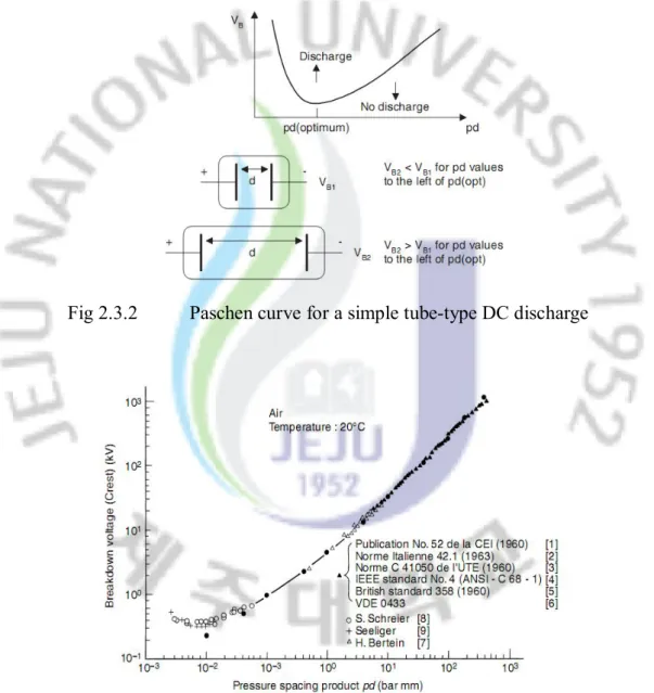
law tells breakdown voltage of parallel plates in a gas is a function of pressure (p) and gap distance (d).
Breakdown voltage V = a (p.d) / ln (p.d) + b
Paschens curve are valid only for electrodes with uniform electric fields.
Fig 2.3.2 Paschen curve for a simple tube-type DC discharge
Figure 2.3.3 Paschen curve for air in log–log scale. Temperature 20 °C. Calculated VB = 6.72√ (pd) + 24.4(pd) [7].
2.4 Corona spark and arc:
There is a difference between corona, spark & arc discharges. To ignite a corona high voltage is required depending upon specific conditions. When the high voltage is sufficient enough then corona transform into spark. And if the power is sufficient enough to sustain a large current for a considerable time then the spark current produces a cathode spot and the spark transformed into arc.
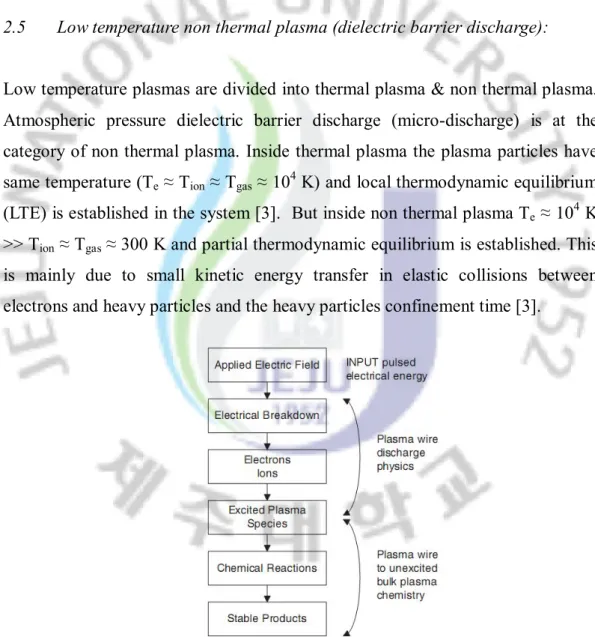
2.5 Low temperature non thermal plasma (dielectric barrier discharge):
Low temperature plasmas are divided into thermal plasma & non thermal plasma. Atmospheric pressure dielectric barrier discharge (micro-discharge) is at the category of non thermal plasma. Inside thermal plasma the plasma particles have same temperature (Te ≈ Tion ≈ Tgas ≈ 104 K) and local thermodynamic equilibrium
(LTE) is established in the system [3]. But inside non thermal plasma Te ≈ 104 K
>> Tion ≈ Tgas ≈ 300 K and partial thermodynamic equilibrium is established. This
is mainly due to small kinetic energy transfer in elastic collisions between electrons and heavy particles and the heavy particles confinement time [3].
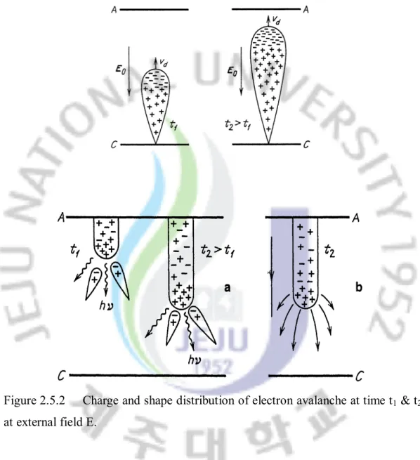
Local plasma is produced due to high electric field and pressure which emits energetic photons. This type of discharge is non stationary and need high voltages at atmospheric pressure [3].
Figure 2.5.2 Charge and shape distribution of electron avalanche at time t1 & t2
at external field E.
Recent modeling indicates streamer branching as non linear process. Short lived discharge filaments grown in-between the electrodes are called micro discharges and usually has duration of 1 – 10 ns, diameter ~ 0.1mm and current density about 102 – 103 Acm-2 [3]. The plasma created from this micro discharge is non thermal plasma and density of electrons ranges from 1014 to 1015 cm-3 and temperature of electron is about 1 to 10 eV [3]. The life cycle of one filament has been shown on Fig 2.5.3.
Figure 2.5.3 The life cycle of one filament. The electron current je generates the excited species A* , which in turn reacts to form the product B. The time scale, τ, of the three processes are very different.
Dielectric barrier discharges DBD are such that one or both of the electrodes are covered with dielectric layers. The plasma ac power is at 10’s Hz to a few kHz. In conventional atmospheric pressure discharges, arcing results in localized heating and nonuniform processing of the gas. In DBD, however, the dielectric surfaces serve the role of a capacitor in series with the plasma. The plasma in DBD consists of a forest of micro streamers. When the micro streamers cross the gap and impinge on the dielectric, the dielectric charges up. Since the transverse mobility of charge on the dielectric is extremely low, the charging of the dielectric is restricted to the local vicinity of the streamer. When the local dielectric charges
and 100’s µm in diameter. Ideally, the streamers randomly appear throughout the discharge volume providing, on the average, uniform plasma.
The discharge characteristics of DBD and average energy of the electrons generated in DBD depend on power input, gap width, frequency, the type of carrier gas and the type of dielectric [3]. Ionization energy of Argon is 15.7596 eV , oxygen 13.6181 eV Zn 9.3942 eV and carbon is 11.2603 eV.
Table 2.2 : Multiplication of electrons in an avalanche at p= 1 atm, in electric fields E and breakdown gap d [4].
Electrodes particularly cathode supply electrons for the initiation, sustaining and for the completion of a discharge. The energy required to remove an electron from a Fermi level is known as the work function Wa and is a characteristic of a given
material showed in Table 2.3 [7].
2.6 Source of energy to release electron:
Photo electronic emission, thermionic emission & field emission are the three ways to supply required energy to release the electron. Field electron emission and the emission current are given by the Fowler-Nordheim formula [4]. In numerical form,
Here εF (V) is the Fermi energy, φ (V) is the work function non perturbed by the field, ξ is a correction factor, and E is measured in V/cm. The reason of field emission is enhancement of the applied field at the microscopic protrusions that always exist on real metal surfaces. Field emission results in the breakdown of vacuum gaps.
In the figure 2.6.1 F - field emission, T - thermionic emission, T + SCH - Schottky-affected thermionic emission, TF - thermionic field emission, F+SCH - Schottky-affected field emission; (a) Mirror forces neglected; (b) mirror forces taken into account. The diagrams illustrate the nature of field-electron and thermionic-field emission, [4].
Electrons in elastic collisions lose little energy and readily build up their kinetic energy supplied by an external source, e.g. an applied field. But in case of inelastic collisions a large fraction of their kinetic energy is transferred into potential energy, causing ionization of the struck molecule. For higher field strength ionization by electron impact is the most important process leading to breakdown of gases. The effectiveness of ionization by electron impact depends upon the energy that an electron can gain along the mean free path in the direction of the field. The mean free path λ of different gases is given in the table 2.4.
Table 2.4 Mean free paths measured at 15°C and 760 Torr [7].
2.7 Reactions inside plasma
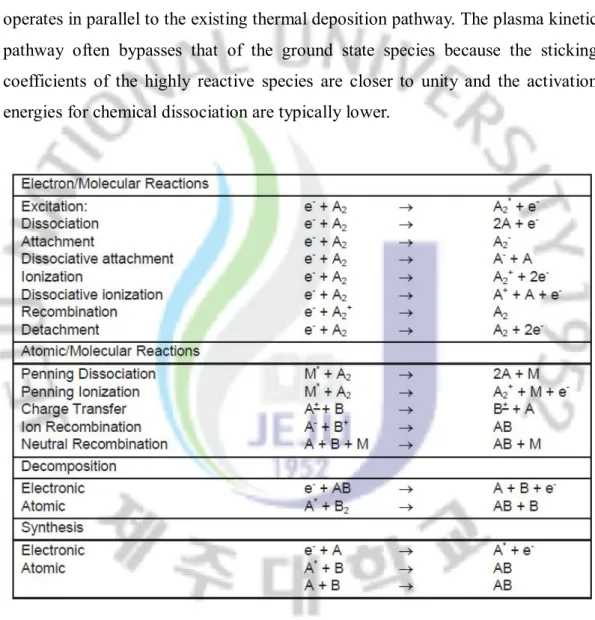
Different types of electron atom collisions happen inside plasma like electron impact ionization, electron impact excitation, electron impact dissociation, electron metastable ionization, metastable neutral ionization, de-excitation, electron ion recombination, radiative recombination, electron attachment and ion - ion recombination. Reactions that could happen inside plasma are given in the table 2.5. If plasma is generated in a Chemical vapor deposition (CVD)
environment, a fraction of the ground-state parent species in the gas phase undergoes electron impact dissociation and excitation, and consequently highly reactive species are also generated. So in addition to the ground state species, these highly reactive species also diffuse to the surface, and undergo similar processes of adsorption, chemical reactions, surface migration, etc. In other words, these highly reactive species follow an alternative deposition pathway which operates in parallel to the existing thermal deposition pathway. The plasma kinetic pathway often bypasses that of the ground state species because the sticking coefficients of the highly reactive species are closer to unity and the activation energies for chemical dissociation are typically lower.
Table 2.5 Probable reactions happened inside plasma.
Consequently, the plasma kinetic pathway makes possible a higher deposition rate. Moreover, the ions present in the plasma may bombard the substrate surface;
bonded reactive species, the surface migration of adatoms, and/or removing undesired contaminants.
Figure 2.7.1 Activation energy diagram for a thermally-driven (solid line) and for a plasma-enhanced (dashed line) reaction [7].
Temperature is still needed to drive the reaction over ΔE* (Figure 2.7.1), i.e. to provide the energy required to promote surface reactions and desorbs byproducts, as well as to lower film contamination.
2.8 Plasma Surface interaction:
The steps of plasma surface interaction are creation of the reactive species within the plasma phase by electron-neutral collisions and subsequent chemical reactions, then transport of the reactive species from the plasma to the substrate. After that adsorption of the reactive species happen on the surface either by physisorption or by chemisorption. The interaction between plasma and substrate surface has been presented in figure 2.7.1 [8].
Figure 2.8.1 Plasma surface interaction diagram [8].
2.9 Optical Emission
Optical emission from plasma occurs primarily due to electron impact excitation of atoms or molecules to an excited state, followed by a relaxation to a lower energy state releasing a photon containing energy equal to the difference between these two energy states. Analysis of the photon energy (wavelength of light) and spectral emission information of species can be used to infer the composition of the species that produced it.
3
EXPERIMENTAL DETAILS
3.1 Experimental configurations:
In the experiment three configurations has been designed, developed & tested to deposit ZnO. They are parallel plate, coaxial, & disk – plate configuration. Most of the parts are common only except the configuration and auxiliaries to hold the electrodes. For example the gas supply section, Zn precursor tank, heating elements AC power supply source are the common elements. Zinc acetyl-acetonate (Zn(C5H7O2)2) has been used as ZnO source. The precursor is heated
inside the tank using electric heater. The temperature maintained inside the tank is about 100 0C. The whole experiment is carried out at atmospheric condition and silicon wafer has been selected as substrate material. The gap between the electrodes was 2 ~ 4 for flat 4 ~ 5.5 for coaxial and for disk plate configuration 5 ~ 7 mm. Oxygen and argon is supplied using Mass flow controller as a carrier & process gas for activation. Gases pass through the glass tube & perforated brass electrode to enter into the non thermal plasma assisted deposition zone. Oxygen flow rate was 100 sccm & Ar flow rate was 0.7 Nl/min. The substrate kept for about 10 minutes inside the non thermal plasma for deposition. For parallel and coaxial type configuration the distance between the electrodes and substrate is about 1 mm. And in disk plate configuration the substrate is kept on the dielectric inside the non thermal plasma environment.
3.2 Parallel plate configuration:
First one is simple parallel plate DBD discharger. In this set up two parallel plates has been placed at variable distance (2~4 mm) a precursor vapor has been supplied through the channel inside the plates. The silicon substrate has been placed under the plates.
Figure 3.2.1 : Schematic diagram for parallel plate configuration.
Figure 3.2.2 : Parllel plate experimental set up.
The distance between the parallel plate electrodes and the substrate was about 1 mm.
3.3 Coaxial plate configuration:
In coaxial configuration two cylindrical shape electrodes has been used inside one is a brass cylinder and the outside electrode is steel mesh. Teflon holder has been designed & manufactured to hold the glass tube & cylindrical electrode. High quality glass tube inside diameter 20 mm and outside diameter 23 mm has been used as dielectric. The gap between the two electrodes was about 4 ~ 5.5 mm and the gap between the dielectric and central electrode was 2.5 ~ 4 mm.
Figure 3.3.1 : Schematic diagram for coaxial electrode configuration
3.4 Disk plate configuration:
In this configuration we have used perforated brass disk of diameter 19.5 mm as one electrode and copper plate sealed (using ceramic sealant) inside ceramic plates used as another electrode, ceramic acts as a dielectric. The distance maintained in between two electrodes are 5~7 mm.
Figure 3.4.1 : Schematic set up of disk plate configuration to deposit ZnO.
The main advantage of this configuration is the substrate is placed inside the plasma environment. So there is more possibility of adsorption & surface chemical reaction. In case of previous two configurations the gas flow is carrying the ionized particles to the substrate (placed outside the plasma production zone). So there is a chance of ionized gas coming in contact with atmospheric gases & cause reduced ionization & reaction rate.
3.5 Equipments used for the measurement:
The equipments used for the measurement and supplying power to the DBD configurations are
1. Power supply (AP Plasma power supply, DOWNSYS) 2. Digital Phosphor Oscilloscope (Tektronix TDS 3054B) 3. Power supply (High voltage amplifier TREK 20/20C) 4. Signal generator (Function generator EZ, FG – 700 2C) 5. X-ray photoelectron spectroscopy (XPS, ESCA 2000) 6. Field Emission scanning electron microscope
7. Optical Emission spectrophotometer (SM – 240 , Spectral Products) 8. Voltage probe (P6015A, Tektronix)
9. Current Probe (P6021 AC current probe, Tektronix)
Two power supply system has been used for the experiment. One power supply has the option to connect signal generator (mentioned in no 3). Frequency and amplitude of the signal can be varied by using the signal generator. Another one (mentioned in no 1) has limited option to change frequency within a very short range from 28.5 KHz to 30 KHz.
4
RESULT AND DISCUSSION
4.1 Optical Emission Spectroscopy of non thermal plasma:
Light emission is a major characteristic of plasmas. Optical emission spectroscopy (OES) has been done to find out the elements present in the non thermal plasma. To emit light, the atoms in the plasma have to be in the excited states. In our experiment collisional excitation is used to excite the atoms in the plasma. Actually in our experiment atoms are in ionization state and an ionization process requires more energy than the excitation process. The elements found by OES are oxygen, argon, carbon, zinc & nitrogen. The measured intensity peaks at particular wavelength has been compared with National Institute Standards and technology (NIST) [9] database to find out the atoms present in the plasma.
Figure 4.1.1 : Emission spectrum of non thermal plasma at visible range at atmospheric condition.
precursor is supplied with oxygen & argon then the two peaks are showing the presence of Zn & carbon (figure 4.1.2).
In this experiment we have also tried to deposit ZnO thin film only using chemical vapor produced from the same precursor but only found deposition when the chemical vapor was enhanced by non thermal plasma generated by dielectric barrier discharge.
Figure 4.1.2 : Emission spectrum of non thermal plasma at visible range while deposition (When gases are supplied).
Origin 8 has been used to plot the Optical emission spectroscopy graphs. In figure 4.1.2 the noise has been subtracted from the original signal to get a clear picture of the prominent intensity peaks.
4.2 Surface analysis of deposited samples:
Deposited samples have been studied using X-ray photoelectron spectroscopy (XPS) to find the chemical constituents present in the thin film. After analysis the presence of Zinc, Oxygen & carbon is evident. The presence of carbon is mainly from the organic precursor.
Figure 4.2.1 : X-ray spectroscopic analysis of deposited ZnO.
The percentage of ZnO present in the sample is about 62.8% in one sample and 59% in another sample. Presence of carbon in the first sample is about 37.2% and 41% in the second sample.
4.3 Surface topography of deposited ZnO thin film:
Field emission scanning electron microscopy (FESEM) has been done to inspect the surface topography and to determine the thickness of the deposited ZnO. The size of the crystals varies from 200 nm to 0.84 μm. Some defects have been observed on the surface. Abnormally high avalanche of electron could be the possible cause of the surface defect. The film thickness ranges from 7 to 9 μm.
Figure 4.3.1 : Surface of ZnO layer on silicon substrate at about 10000 times magnification.
4.4 Voltage and current characteristic:
Voltage and current behavior has been observed of different DBD configurations. Voltage and current characteristics with changing time has been represented in the figures below for different configurations. All the graphs have been plotted for voltage 9 KV frequency 28.5 KHz.
Figure 4.4.1 Voltage current relationship with time of Parallel plate DBD.
Figure 4.4.3 Voltage current relationship with time of Coaxial type DBD.
The transient nature is vivid from all the three graphs. The amplitude of current is less in case of disk plate configuration but the current line is showing that current amplitude variation range is more. The fluctuation of current indicates breakdown of gases. In case of disk plate configuration breakdown is happening along the complete voltage cycle but in case of other two configurations breakdown is mostly confined to a region when the voltage is increasing either in positive or negative direction.
4.5 Relation between Frequency and breakdown voltage:
type configuration (gap between two electrodes is 4 mm).
Figure 4.5.2 Relation between Frequency and Breakdown voltage in coaxial type configuration (gap between two electrodes is 5.5 mm).
Figure 4.5.3 Relation between Frequency and Breakdown voltage in disk plate type configuration.
Study relating frequency and breakdown voltage reveals the fact that for coaxial type configuration breakdown voltage increase with frequency but for the disk plate configuration the relationship is not linear. The optimum frequency is 29 KHz in the frequency range 28.5 KHz to 30 KHz. Due to the limitation of the power supply to change the frequency at a wider scale it was not possible to check the other frequencies. In case of coaxial type it’s quite natural that the breakdown
4.6 Dependence of deposition thickness on electrode gap:
Experiment has been performed to observe consequence of electrode distance on ZnO deposition for disk plate configuration. The deposition has been done maintaining O2 flow rate 100 sccm, Ar flow rate 1 Nl/min, Temperature of
precursor tank 98 ~102 0C, 5 KV at frequency 29 KHz for about 10 minutes.
Figure 4.6.1 Deposition thickness increases with electrode distance.
The deposition thickness increases with electrode distance. As the sample is placed inside the plasma assisted zone the possible reason could be longer distance allows more excitation and ionization that ultimately affects deposition rate. But the deposition is not uniform throughout the sample. There are some localized deposition spots which have higher thickness. The deposition thickness is measured by using FESEM.
5
SUMMARY AND CONCLUSION
5.1 Summary
The total experiment has been performed to deposit ZnO thin film on silicon substrate using dielectric barrier discharge. The process is one kind of activated reactive evaporation (ARE) where dielectric barrier discharge has been used to produce plasma species. As electrode configuration and geometry has great impact on deposition we have tried with three different configurations. Best result was achieved with coaxial and disk plate configuration. No deposition has been observed using parallel plate configuration only except condensation. Surface analysis done by XPS has confirmed that the deposited sample contained about 62.8% ZnO. The presence of carbon inside the samples was not unexpected but the presence of carbon is undesirable for conductive ZnO thin film. The experiment shows that it is possible to deposit ZnO using dielectric barrier discharge. The size of the crystals varies from 200 nm to 0.84 μm in size and the thickness is about 7 to 9 μm. The elements found by OES are oxygen, argon, carbon, zinc & nitrogen. Carbon species has evolved from the organic precursor.
5.2 Conclusion
Many researchers have successfully deposited ZnO using various plasma enhanced deposition techniques but a successful atmospheric pressure technique which involves dielectric barrier discharge is still a region which needs exploration. The main objective of our experiment was to deposit ZnO thin film using non thermal plasma generated by dielectric barrier discharge at atmospheric condition. Three different configurations have been adopted to achieve deposition. Among the three configurations coaxial and disk plate type configuration gives the best result over parallel plate configuration. Optical emission spectroscopy (OES) has been done to find out the elements present in the non thermal plasma.
of carbon determined by OES gives some indication that there is good chance to have some carbon deposit inside the sample. X-ray photoelectron spectroscopy has confirmed the presence of ZnO including carbon deposition.
5.3 Future Work
This work has lot of possibilities and vast field to discover. The works that could be done is stated below
Ø Optimizing deposition parameters and conditions for better process control. Ø Reduction of carbon content using different techniques and different
precursors.
Ø Establishing mathematical variables to explain the process.
Ø Mathematical modeling and simulation for better understanding and prediction.
Ø Combining this process with different plasma generation and excitation technique (for example introducing radio frequency and microwave) to get better result and control.
6
REFERENCES
[1] Hifan Liang. Roy G. Gordon J Mater Sci (2007) 42:6388-6399 “Atmospheric pressure chemical vapor deposition if transparent conducting films of fluorine doped Zinc oxide and their application to amorphous silicon solar cells”
[2] M. Miclea, K. Kunze, G. Musa, J. Franzke, K. Niemax, The dielectric barrier discharge – a powerful microchip plasma for diode laser spectrometry, Spctrochimica Acta Part B 56 (2001) 37 – 43.
[3] A. Dinklage T. Klinger G. Marx L. Schweikhard, Plasma physics, confinement transport & collective effects, Springer.
[4] Yuri P. Raizer, Gas discharge physics, Springer-Verlag.
[5] Pieter Heyse, Roel Dams, Sabine Paulussen, Kristof Houthoofd, Kris Janssen, Pierre A. Jacobs, Bert F. Sels, Dielectirc barrier discharge at atmospheric pressure as a tool to deposit versatile organic coatings at moderate power input. Plasma Processes and polymers 2007, 4 , 145 – 157.
[6] E. Kuffel, W.S. Zaengl, J. Kuffel, High Voltage Engineering Fundamentals, second edition.
[7] Stephen M. Rossnagel, Jerome J. Cuomo, William D. Westwood, Handbook of Plasma Processing Technology.
[8] Francis F. Chen and Jen P. Chen, Lecture notes on Principles of plasma processing Plenum/Kluwer Publishers 2002.
[10] Oleksiy V. Penkov, Vadim Yu Plaksin, Min Gook Ko, Chanjoo Yim and Heon Ju Lee, Journal of the Korean Physical society 53, (Nov 2008)
![Table 2.1 Influence of plasma on three steps of film deposition by ARE process[7]](https://thumb-ap.123doks.com/thumbv2/123dokinfo/4762360.14775/18.892.158.782.325.781/table-influence-plasma-steps-film-deposition-process.webp)


![Table 2.2 : Multiplication of electrons in an avalanche at p= 1 atm, in electric fields E and breakdown gap d [4]](https://thumb-ap.123doks.com/thumbv2/123dokinfo/4762360.14775/25.892.158.766.222.1000/table-multiplication-electrons-avalanche-atm-electric-fields-breakdown.webp)
![Table 2.4 Mean free paths measured at 15°C and 760 Torr [7].](https://thumb-ap.123doks.com/thumbv2/123dokinfo/4762360.14775/27.892.154.800.302.941/table-mean-free-paths-measured-c-torr.webp)