Carbon
Carbon NanomaterialsNanomaterials Design Laboratory (CNDL)Design Laboratory (CNDL)
Science and Engineering of Science and Engineering of
Organic
Organic Nanomaterials Nanomaterials
Carbon
Carbon NanomaterialsNanomaterials Design Laboratory (CNDL)Design Laboratory (CNDL)
Part I. Fundamentals:
Part I. Fundamentals:
Basics For Designing Basics For Designing Organic
Organic Nanomaterials Nanomaterials
Carbon
Carbon NanomaterialsNanomaterials Design Laboratory (CNDL)Design Laboratory (CNDL)
Part I. Fundamentals:
Part I. Fundamentals:
Basics For Designing Organic
Basics For Designing Organic NanomaterialsNanomaterials
Chapter 1. Physical Properties of Chapter 1. Physical Properties of
Organic
Organic Nanomaterials Nanomaterials
Carbon
Carbon NanomaterialsNanomaterials Design Laboratory (CNDL)Design Laboratory (CNDL)
What Is Nanoscale ?
Carbon
Carbon NanomaterialsNanomaterials Design Laboratory (CNDL)Design Laboratory (CNDL)
Definition
the systematic manipulation of matter on the length scale 1-100 nm to produce useful new engineered structures, materials, or devices.
History
- R. Feynman, 1959, “There’s plenty of room at the bottom”
- Kroto, Smalley, Curl, 1985, synthesis of Fullerene, C60
- Sumio Iijima, 1991, discovery of single wall carbon nanotube
Nanotechnology today
- 1600 companies, 700 industrial products - world-wide investment of 4.8 billion $ / yr
The U.S. National Nanotechnology Initiative (NNI) - first passed in 2001
- now ~ 1 billion $ / yr
- optimistic status report: May 2005
- four phases envisioned (now in phase 1)
The Nanotechnology Movement
© Hyperion catalysis website
about 1/1000 width of human hair
Carbon
Carbon NanomaterialsNanomaterials Design Laboratory (CNDL)Design Laboratory (CNDL)
Nanotechnology is the development of….
Nanoparticles
- buckminster fullerene C60
- metallic nanoparticles (gold, silver, iron, etc) - glass/ceramic nanoparticles (titania, silica, etc) - quantum dots (semiconductor nanoparticles)
Nanotubes, nanofibers, nanowires
- carbon nanotubes
- nanofibers (carbon, polymer, ceramic) - nanowires (metallic, semiconducting)
Nanoplatelets
- graphite, clay,
- silica, hydroxyapatite
Nanostructured surfaces Nanostructured solids
and their application as
components for next-generation technologies, including:
batteries, fuel cells, sunscreens, cosmetics, structural materials, implants, drug delivery vehicles, catalysts, sorbents, and
much, much more…….
Carbon
Carbon NanomaterialsNanomaterials Design Laboratory (CNDL)Design Laboratory (CNDL)
0-D materials 1-D materials 2-D materials
metals
semiconductors
ceramics
carbons
polymers
other
The Nanomaterial Matrix
(some well-known examples)
Au nanoparticles Fe magnetic nanoparticles
nanopart. catalysts (Pt,Zn,Cu,Ni,Co…) quantum dots
nanophase powders for low-T sinterable coatings, parts, composite fillers, sorbents
oligomers (e.g. chitosan) branched compounds (dendrimers)
surfactant assemblies (liposomes)
nano-clays
fullerenes, carbon black, nanohorns carbon nanotubes,
nanofibers nano-graphite semiconducting
nanowires, nanorods nanowires
electrospun ceramic nanofibers for composite fillers
electrospun polymer nanofibers biodegradable polymer nanobeads
for medical applications
Carbon
Carbon NanomaterialsNanomaterials Design Laboratory (CNDL)Design Laboratory (CNDL)
General Properties of
General Properties of Nanoscale Nanoscale System System
Carbon
Carbon NanomaterialsNanomaterials Design Laboratory (CNDL)Design Laboratory (CNDL)
Bulk Vs. Surface
Carbon
Carbon NanomaterialsNanomaterials Design Laboratory (CNDL)Design Laboratory (CNDL)
Bulk Vs. Surface
nano 103
10-9 ~ 10-8
meso 107
10-8 ~ 10-6
Cluster molecule
<102
<10-9
macro 1010
10-6 ~ 10-5
macro
>1014
> 10-5
Feature Surface
atoms (%)
# of Size (nm) atom
Carbon
Carbon NanomaterialsNanomaterials Design Laboratory (CNDL)Design Laboratory (CNDL)
Surface Ratio
Carbon
Carbon NanomaterialsNanomaterials Design Laboratory (CNDL)Design Laboratory (CNDL)
Electrical Property
Carbon
Carbon NanomaterialsNanomaterials Design Laboratory (CNDL)Design Laboratory (CNDL)
Transport Properties of Nano-scale Materials
Carbon
Carbon NanomaterialsNanomaterials Design Laboratory (CNDL)Design Laboratory (CNDL)
Transport Properties of Nano-scale Materials
Carbon
Carbon NanomaterialsNanomaterials Design Laboratory (CNDL)Design Laboratory (CNDL)
Feature of Nanoscale System
Carbon
Carbon NanomaterialsNanomaterials Design Laboratory (CNDL)Design Laboratory (CNDL)
In Nanoscale System
Newton mechanics – particle deterministic description Blackbody radiation
Photoelectric effect Compton effect Atomic spectra
Introduction of quantized concept
Unsolved problem
Quantum size effect
As the size of system decrease, new effects begin to appear - # of charge carrier
n type semiconductor, nd = 1018/cm3
but in nanosystem, nd = 1/(10nm)3 only one electron - density n states 1,2,3 dimension
Carbon
Carbon NanomaterialsNanomaterials Design Laboratory (CNDL)Design Laboratory (CNDL)
In Nanoscale System
(Quantum size effect)
Density of state (DOS)
Carbon
Carbon NanomaterialsNanomaterials Design Laboratory (CNDL)Design Laboratory (CNDL)
10 nm
Fe3O4, Magnetite
Size-dependent Magnetism
Size-Dependent Emission
CdSe Semiconductor
50 nm
Nanogold on Silica
Size-dependent Absorption
HALAS, WEST
In Nanoscale System
(Quantum size effect)
Carbon
Carbon NanomaterialsNanomaterials Design Laboratory (CNDL)Design Laboratory (CNDL)
Two Approach in Nanotechnologyn
• Fabrication of nanomaterials/nanodevices by lithography
• Ultrahigh density device fabrications
• Complicated and of high cost
• Use of limited materials due to material compatibility
• Fabrication of nanodevices by simple assembly of nanomaterials
• Numerous types of nanodevices
• Use of numerous nanomaterials
(Carbon nanotubes, semiconductor nanocrystals and nanowires/nanorods, etc)
Carbon
Carbon NanomaterialsNanomaterials Design Laboratory (CNDL)Design Laboratory (CNDL)
Nanotechnology & Nanomaterials
Top-down devices
Bottoms-up materials
Ultra-fine particles Carbon black
Colloid Silica Historical
Carbons Inorganic materials Polymers Composition
Nanocomposites Nanotubes Nanocrystals
Format
Nanopores
Classification
Carbon
Carbon NanomaterialsNanomaterials Design Laboratory (CNDL)Design Laboratory (CNDL)
…
Nano lithography / Patterning
Bulk Materials Nano-scale structures
• E-beam lithography
• Nanoimprint Technology KrF
(λ = 248 nm)
ArF (λ = 193 nm)
F2
(λ = 157 nm)
EUV (λ = 11.4 nm)
Conventional Lithography
Nanolithography
• Probe Technology
Demand
High controllability High cost
Top-down Approach
R. Feynman, 1959,
“There’s plenty of room at the bottom”
Carbon
Carbon NanomaterialsNanomaterials Design Laboratory (CNDL)Design Laboratory (CNDL) Nano-scale materials
Nucleation / Growth
Atoms / Molecules Nano-scale structures
Cost effective
Low controllability
Self-assembly
• Colloid process
• Thin film technology
• Gas phase nucleation
Size Distribution Areal Density Distribution
Nucleation, Growth & Self-assembly
Bottom-up Approach
Carbon
Carbon NanomaterialsNanomaterials Design Laboratory (CNDL)Design Laboratory (CNDL)
Introduction to Solid State Physics
Introduction to Solid State Physics
Carbon
Carbon NanomaterialsNanomaterials Design Laboratory (CNDL)Design Laboratory (CNDL)
long range Vs. short range order
crystal glass gas
crystals: constituents fall into regular, repeated 3D patterns long range order and short range order
anisotropic geometry anisotropic properties other solids: amorphous
examples: glass, some plastics, etc.
statistically isotropic on a long range anisotropic on a short range
possibly short range order
Carbon
Carbon NanomaterialsNanomaterials Design Laboratory (CNDL)Design Laboratory (CNDL)
Line lattice
Plane lattice
aa b γ
Lattice Structures
Crystal axis Unit cell
Carbon
Carbon NanomaterialsNanomaterials Design Laboratory (CNDL)Design Laboratory (CNDL)
Crystal structure = Lattice + Basis
Basis
a
b
A atom
C atom B atom
+
Lattice point
Triclinic Monoclinic
Orthorhombic
Tetragonal Hexagonal
Cubic Trigonal
7-crystal system
Carbon
Carbon NanomaterialsNanomaterials Design Laboratory (CNDL)Design Laboratory (CNDL)
14 Bravais Lattices
Carbon
Carbon NanomaterialsNanomaterials Design Laboratory (CNDL)Design Laboratory (CNDL)
Closed Packed Structures
Layer Stacking sequence Layer Stacking sequence
2D Hexagonal Packing
3D ABABABABAB (HCP)
3D ABCABCABC (FCC)
Carbon
Carbon NanomaterialsNanomaterials Design Laboratory (CNDL)Design Laboratory (CNDL)
Interstitial Sites ; FCC structure
Octahedral sites ; 4
Octahedral sites ; 4 Tetrahedral sites ; 8Tetrahedral sites ; 8
The number of octahedral sites is equal to the number of spheres The number of tetrahedral sites is double of the number of spheres
Carbon
Carbon NanomaterialsNanomaterials Design Laboratory (CNDL)Design Laboratory (CNDL) 8 )
, 5 0 , 0 (
Tetrahedral sites ; 4 Tetrahedral sites ; 4
8 ) , 1 3 , 2 3 (1 8)
, 3 0 , 0
( )
8 , 7 3 , 2 3 (1
Interstitial Sites ; HCP structure
Carbon
Carbon NanomaterialsNanomaterials Design Laboratory (CNDL)Design Laboratory (CNDL)
In FCC, the relation between layers and atom number
The number of atoms on the surface is
Structural magic number
Carbon
Carbon NanomaterialsNanomaterials Design Laboratory (CNDL)Design Laboratory (CNDL)
Lattice Vibrations
In reality, a crystal undergoes continuous fluctuations in the neighborhood of their regular positions in the lattice. These fluctuations arise from the heat or thermal energy in the lattice, and become more pronounced at higher temperatures.
Normal modes : Lattice’s own characteristic modes or frequencies of vibration, and the overall collective vibrational motion of the lattice is a combination or superposition of many normal modes
Acoustic modes : low-frequency mode
Optical modes : high-frequency mode
Carbon
Carbon NanomaterialsNanomaterials Design Laboratory (CNDL)Design Laboratory (CNDL)
Diatomic vibration
(acoustical and optical branches)
(ref) http://www.chembio.uoguelph.ca/educmat/chm729/Phonons/optmovie.htm
Transverse acoustical mode for diatomic vibration
Transverse optical mode for diatomic vibration
Carbon
Carbon NanomaterialsNanomaterials Design Laboratory (CNDL)Design Laboratory (CNDL)
1-D Lattice with Diatomic Atom
Consider a linear diatomic chain of atoms (1-D model for a crystal like NaCl):
In equilibrium:
M1
a
M2 M1 M2
Applying Newton’s second law and the nearest-neighbor approximation to this system gives a dispersion relation with two “branches”:
2 / 1
2 2 1 2
1 2 1 2
2 1
2 2 1
1 2
1
2 1
1
2
4 sin ( )
⎥ ⎥
⎦
⎤
⎢ ⎢
⎣
⎡ ⎟⎟ ⎠ −
⎜⎜ ⎞
⎝
⎛ +
⎟⎟ ±
⎠
⎜⎜ ⎞
⎝
⎛ +
= ka
M M
c M
M
M c M
M M
M c M
ω
ω-
(k) ω
Æ0 as k (=2π/λ) Æ 0 acoustic modes (M
1and M
2move in phase)
ω+(k) ω
Æ ωmaxas k Æ 0 optical modes (M
1and M
2move out of phase)
Carbon
Carbon NanomaterialsNanomaterials Design Laboratory (CNDL)Design Laboratory (CNDL)
These two branches may be sketched
schematically as follows:
gap in allowed frequencies
k
ω
a π a
− π
0
optical
acoustic
In a real 3-D solid the dispersion relation will differ along different directions in k-space. In general, for a p atom basis, there are 3 acoustic modes and (p-1) groups of 3 optical modes, although for many propagation directions the two transverse modes (T) are degenerate.
1-D Lattice with Diatomic Atom
Carbon
Carbon NanomaterialsNanomaterials Design Laboratory (CNDL)Design Laboratory (CNDL)
Phonon
hω Energy
Distance
Equilibrium distribution
1 exp
1
⎟⎟−
⎠
⎜⎜ ⎞
⎝
= ⎛
T k n
B
hω
• where ħw can be thought as the energy of a particle called phonon, as an analogue to photon
• n can be thought as the total number of phonons with a frequency w, and follows the Bose-Einstein statistics:
h ω
⎟ ⎠
⎜ ⎞
⎝ ⎛ +
= 2
n 1 u
•The linear atom chain can only have N discrete K Æ w is also discrete
• The energy of a lattice vibration mode at frequency w was found to be
Carbon
Carbon NanomaterialsNanomaterials Design Laboratory (CNDL)Design Laboratory (CNDL)
conductivity of solids varies strongly:
•Cu r=1.7x10
-8W (good conductor)
•quartz r=7.5x10
17W (good insulator)
•explanation: electron bands!
internuclear distance
energy
example: 2 Na atoms
Na+Na Na
2molecular IP
atomic IP
1 attractive
and 1 repulsive state
Band Theory of Solids
Carbon
Carbon NanomaterialsNanomaterials Design Laboratory (CNDL)Design Laboratory (CNDL) internuclear distance
energy
attractive
repulsive
overlapping wave functions lead to splitting of the state”:
•attractive state: more electron density between atoms, more screening
•repulsive state: less electron density between atoms, less screening
Band Theory of Solids
Carbon
Carbon NanomaterialsNanomaterials Design Laboratory (CNDL)Design Laboratory (CNDL)
as many states as atoms involved!
5 Na atoms:
energy
internuclear distance
Band Theory of Solids
“continuous”energy band of closely spaced levels 10
23Na atoms:
internuclear distance
Carbon
Carbon NanomaterialsNanomaterials Design Laboratory (CNDL)Design Laboratory (CNDL)
electron bands and forbidden bands
“atomic” state
overlapping bands empty band
filled bands
conductor“atomic” state filled band
partially filled band
conductor
Î
FÎ
F“atomic” state forbidden band
“gap”
empty band
filled bands
Î
Fsemiconductor or insulator
“small” gap (~1 eV):
semiconductor
“large” gap (several eV):
insulator
Carbon
Carbon NanomaterialsNanomaterials Design Laboratory (CNDL)Design Laboratory (CNDL)
conductors:
•valence band is either only partially filled or overlaps with an empty band
•an electric field accelerates electrons
•with their increased energy they still “fit” into the empty part of the band
•conductors are opaque insulators:
•valence band is filled, the gap to the empty band is several eV
•electrons cannot overcome this gap thermally
•the electric field has to reach 10
8V/m to overcome the gap (smaller fields are insufficient because of collisions)
•the material is called insulator
•insulators are usually transparent
electron bands and forbidden bands
Carbon
Carbon NanomaterialsNanomaterials Design Laboratory (CNDL)Design Laboratory (CNDL)
T~0 K:
•semiconductors and insulators have almost identical resistivity room temperature
•in semiconductors a tiny fraction of electrons can be thermally excited over the gap to the empty band
•the few electrons are sufficient to allow small current flows in the presence of a field E
“gap”
almost empty band, conduction band
almost filled band, valence band
Î
FSemiconductors
Carbon
Carbon NanomaterialsNanomaterials Design Laboratory (CNDL)Design Laboratory (CNDL)
Î
Fn-type:
• replace few Si atoms by e.g. As
• Si has 4 valence electrons needed for covalent bond
• As has 5 valence electrons 1 excess electron
• excess electron needs fractions of eV to reach the conduction band
• excess electron state is called donor level
• Fermi energy is raised towards the conduction band
p-type:
• same principle, but one electron too little
• e.g. replacement of Si by Ga
• excess vacancy, excess hole
• electron from the valence band can easily reach the so called acceptor levels
donor levels
Î
Facceptor levels
Doping
Carbon
Carbon NanomaterialsNanomaterials Design Laboratory (CNDL)Design Laboratory (CNDL)
Exciton
An exciton is a bound state of an electron and an imaginary particle called an electron hole in an insulator or semiconductor, and such is a Coulomb-correlated electron-hole pair. It is an elementary
excitation, or a quasiparticle of a solid.
1. photon enters a semiconductor
2. exciting an electron from the valence band into the conduction band.
3. The missing electron in the valence band leaves a hole behind, of opposite electric charge, to which it is attracted by the Coulomb force.
4. The exciton results from the binding of the electron with its hole;
as a result, the exciton has slightly less energy than the unbound electron and hole.
Carbon
Carbon NanomaterialsNanomaterials Design Laboratory (CNDL)Design Laboratory (CNDL)
Excitons
(bound electron-hole pairs)
SEMICONDUCTOR PICTURE
GROUND STATE WANNIER EXCITON
binding energy ~10meV radius ~100Å
( )
( )
⎭⎬⎫⎩⎨
⎧
= +
=
h e
e ex
m m m m
n eV m E m
/ 1
/ / 6 . 13
* 2 2 0
0
*
ε ε
fig. 2.20
Carbon
Carbon NanomaterialsNanomaterials Design Laboratory (CNDL)Design Laboratory (CNDL)
Various Organic
Various Organic Nanomaterials Nanomaterials : Its Physical Properties
: Its Physical Properties
CNDL
Part Ⅰ . Fundamentals:
Basics for Designing Organic Nanomaterials
Chapter 1. Physical Properties of Organic Nanomaterials
Chapter 2. Design of Nanomaterials based on Microemulsion Physics Chapter 3. Design of Nanomaterials based on Sol-gel Chemistry
Chapter 4. Design of Nanomaterials based on Vapor Processing
Chapter 5. Design of Nanomaterials based on Macromers and Block
Copolymers
CNDL
Chapter 1. Physical Properties of Organic Nanomaterials
1.1. Introduction to nanomaterials
1.2. Size-dependant Properties 1.2.1. Melting points
1.2.2. Magnetism
1.2.3. Optical properties - Color 1.2.4. Conductivity
1.3. Applications 1.3.1. Colors 1.3.2. Catalysis
1.3.3. Nanoelectronics
CNDL
1.2. Size-dependant Properties
To demonstrate quantum size effects experimentally, appropriate materials are needed.
In the course of the last 10-15 years there has been remarkable progress in
preparing metal clusters in the size range of less than one nanometer up to dozens of nanometers.
Here, only some selected examples are given that have turned out to exhibit well- established size-dependent properties
CNDL
1.2.1. Melting points
1.2. Size-dependant Properties
Assumption
: A property is not directly dependent on the electronic situation in the particles, but is rather a consequence of the averaged coordination number of the participating atoms.
: The majority of metals form hexagonal or cubic close-packed structures with coordination numbers of 12.
: The coordination numbers of the surface atoms are 9 or smaller, depending on faces and kind of faces, edges, or corners.
Bulk vs. Nanoparticles
- Bulk materials the surface atoms form a negligible part of the total number of atoms
- The smaller particles the proportion of surface atoms increases
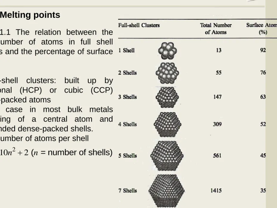
The information on the percentage of surface atoms in close-packed full-shell clusters of different sizes. Table 1.1
(Ex. A spherical particle of 50nm in diameter only about 6% of surface atoms)
CNDL
1.2.1. Melting points
1.2. Size-dependant Properties
Table 1.1 The relation between the total number of atoms in full shell clusters and the percentage of surface atoms
- Full-shell clusters: built up by hexagonal (HCP) or cubic (CCP) closed-packed atoms
- The case in most bulk metals consisting of a central atom and surrounded dense-packed shells.
- The number of atoms per shell
: 2
10n 2 ( = number of shells)n
CNDL
1.2.1. Melting points
1.2. Size-dependant Properties
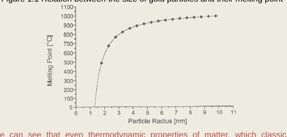
The melting point of solid is reached when the order of the lattice is beginning to be destroyed.
Bulk vs. Nanoparticles
- Bulk : For a distinct solid, the melting point is a physical constant.
- Nanoparticles : When the number of surface atoms becomes equal to or even exceeds the number of inner-core atoms, the melting process starts earlier.
As the coordination number of surface atoms is 9 or smaller, these atoms are more easily rearranged than those in the center of the particles.
In Figure 1.1, the relation between particle size and melting point of gold particles is shown, calculated by the method of Reifenberger. Ref.2-1
: dramatic decrease of melting points for particles smaller than 3-4 nm
CNDL
1.2.1. Melting points
1.2. Size-dependant Properties
Figure 1.1 Relation between the size of gold particles and their melting point
We can see that even thermodynamic properties of matter, which classically described are natural constants, change with the dimension of the material.
CNDL
1.2.2. Magnetism
1.2. Size-dependant Properties
Diamagnetic materials have only spin-paired electrons.
In practice a macroscopic piece of a diamagnetic metal can have one or unpaired electrons. No way to measure because of the effectively infinite number of atoms and electrons.
However, the particle size small enough to make one unpaired electron measurable the predicted so-called “odd-even effect” become visible
※ Odd-even effect : Among small diamagnetic metal particles, there should be a 50:50 distribution of odd and even numbers of electrons
Details in Chapter 2
CNDL
1.2.2. Magnetism
1.2. Size-dependant Properties
►Example◄
Y.VOLOKITIN, J.SINZIG, L.J.DE JONGH, G.SCHMID, M.N.VARGAFTIK and I.I.MOISEEVI,
Nature, 1996, 384, 621
CNDL
Metals can be polarized by electromagnetic irradiation exciting electrons.
Considering the ideal case of an undamped oscillation of free electrons in a defect-free metal lattice, the solution of the wave eq. results in an expression for the complex refractive index n:
Appendix 1-1
The refractive index is related to the reflectivity Rv of a metal by the Beer equation.
1.2.3. Optical properties - Color
1.2. Size-dependant Properties
2 2
2 0
1 E
e
n e N
m v
2 2
2 2
( ' 1) ( ' 1)
v
n k
R
n k
NE : the density of electrons me : electronic mass
v : frequency of the electromagnetic irradiation ε0 : dielectric constant of vacuum
k : absorption coefficient
n’ : real part of the complex refractive index n = n’(real part) + n’’(imaginary part)
CNDL
1.2.3. Optical properties - Color
1.2. Size-dependant Properties
2
0 E P
e
v e N
m
If v is small enough n2 <0 (n consists of only the imaginary part n’’ n’=0
the refractivity R=1 : reflect electromagnetic irradiation totally
Higher frequencies n’>1 with k=0 (nonabsorbing metals)
n≈1 and R≈0 : ideal metals under these conditions become transparent (for instance, alkali metals in the near UV-region)
The limiting or plasma frequency vp for the transition R=0 R=1 for free electron
If metal particle size is reduced the mean free path of the electrons exceeds the particle’s radius electrons can be excited by visible light to perform fluidlike plasmon oscillations : Mie theory
The dipole and higher multiple moments are caused by surface charging (especially effective for spherical shapes)
light
electric field
surface charges
++ + + +
- -
- - -
CNDL
1.2.3. Optical properties - Color
1.2. Size-dependant Properties
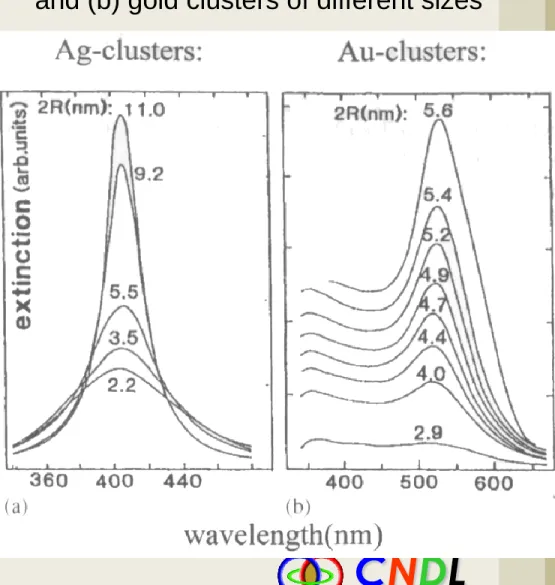
As can be seen from Figure 1.3 , the varying intensity of the plasmon resonances depends on the cluster size.
Decreasing particles size increasing damping the electronic relaxation after electromagnetic excitation is accelerated reduced life time of the plasma excitation broadening of the lines.
Figure 1.3 Absorbance spectra of (a) silver and (b) gold clusters of different sizes
CNDL
1.2.3. Optical properties - Color
1.2. Size-dependant Properties
The above-mentioned optical properties refer to isolated nanoparticles. In practice, the particles often cannot be considered as independent from each other.
Aggregates of clusters effect shifts of the plasmon resonances depending on their topologies.
The orientation of the dipoles of connecting particles results in two individual vibrations of the optical excitation. Fig 1.4
Excitation along the row causes a long-wave shift, whereas perpendicular excitation results in a high-energy shift. detail in chapter 2
The optical properties of such particle arrangements are a complex combination of properties of the particles, of the electronic environment, and of dispersion and arrangement.
Figure 1.4 Eigenmodes of an idealized chain of colloids. (a) longitudinal (b) transverse eigenmode
CNDL
1.2.4. Conductivity
1.2. Size-dependant Properties
4 0 e F
e m V
If the conduction band of metal is only partially occupied by electrons, they can move without resistance in perfect metallic crystal lattice. But they are scattered by the wave character of the electrons.
The mobility of electrons :
Mean time between two collisions τ = λ/ Uf
Ex) Copper at RT : Uf = 1.6 x 10⁶ ms-1, λ = 4.3 x 10⁻⁸m. ∴ τ = 2.7 x 10⁻¹⁴s
Scattering mechanisms : 1) dislocation, stacking disorders, ETC
2) scattering at thermal vibrations of lattice (phonon)
Ohm’s law describes the linear relation between U and I in bulk metal ; U = IR
where, λ = mean free path between collisions me= effective mass of the electron
Uf= speed of the electrons (Fermi speed) ε0= dielectric constant of vacuum
CNDL
1.2.4. Conductivity
1.2. Size-dependant Properties
The band structure begins to change if the dimension of a metal particle becomes small.
→ Ohm’s law is no longer valid.
→ Single nanoparticles have to be investigated.
To avoid contact resistance, two capacitances between electrodes and object are used.
Figure 1.4 Experimental conditions for recording a current (I)-voltage (U) characteristic of a single nanoparticle. The capacitances between tips and cluster are formed by the ligand shell
CNDL
1.2.4. Conductivity
1.2. Size-dependant Properties
, C QH
QH
E h
R C
Coulomb 2 U e
C
Quantum mechanically describe by the quantum Hall resistance RQH and the capacity of the particle
→ Ref. 2-2
The current-voltage characteristic for an ideal quantum dot shows no current up to
Following this an electron tunneling process occurs if the Coulomb energy of the quantum dot is compensated by external voltage of U = ± ne/(2C)
Figure 1.5 I-U characteristic of ideal single electron transport
CNDL
1.2.4. Conductivity
1.2. Size-dependant Properties
FIGURE 1.6 Scanning electron microscopic image of a 17nm ligand-stablized palladium cluster, trapped between two platinum tips. Appl. Phys. Lett., 1997,
71, 1273.
SEM image of an experiment
17nm palladium particle is trapped between two PT tips, separated from them by a thin shell of organic molecules(p-H2N- C6H4-SO3Na).
CNDL
1.2.4. Conductivity
1.2. Size-dependant Properties
FIGURE 1.7 I-U characteristics of the 17nm palladium cluster. At 295K it behaves in a bulklike manner, following Ohm’s law. At 4.2K a pronounced Coulomb blockade is observed.
Appl. Phys. Lett., 1997, 71, 1273.
At 295K, there is a linear relation between I and U, corresponding to Ohm’s law.
At 4.2K, a typical Coulomb gap of
~55mV is observed, indicating that the condition kT<<e2/2C is fulfilled.
To make quantum size behavior of small metal particles available at RT we have to further reduce their size, as the capacitance C of the particles depends directly on their diameter.
I-U characteristic of the 17nm palladium
CNDL
1.2.4. Conductivity
1.2. Size-dependant Properties
I-U characteristic of the 1.4nm gold particle
The gold cluster compound Au55(PPh3)12Cl6 shows typical Coulomb blockade even at RT
FIGURE 1.8 I-U characteristics of a ligand-stabilized Au55 cluster at room temperature. Appl. Phys. A. 1998, 66, 189
CNDL
1.2.4. Conductivity
1.2. Size-dependant Properties
The electronic conductivity of many clusters in a row results from tunneling processes between them through the ligand shells, leading to electronic intercluster bands by resonant tunneling.
The electronic conductivity of many clusters in a row results from tunneling process, leading to electronic intercluster bands by resonant tunneling.
Idealized cluster conduct electrons without resistance.
FIGURE 1.9 Scheme of the energy levels of a Au55(PPh3)12Cl6 cluster. In the ground state the diameter of the 1.4 nm Au55 core corresponds to λ/2 (λ: de Brolie wavelength). The excited state
enables electron tunneling through the ligand shell.
FIGURE 1.10 Ideal cluster wire with tunneling conditions
CNDL
1.2.4. Conductivity
1.2. Size-dependant Properties
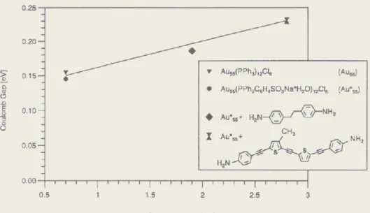
The relationship between distances and activation energies
If the distances are extended by thicker ligand shells or by spacer molecules, the activation energies increase.
FIGURE 1.11 Correlation between cluster spacing and Coulomb gap of variously ligand Au55clusters.
CNDL
1.3.1. Colors
1.3. Applications
A very obvious property of nanoparticles, at least of some metals, is their specific color.
1) Gold colloids color glasses
ex) ruby glass : finely dispersed gold colloids
2) silver, copper attractive colors in glassy materials
The use of alloys in particular has broadened the availability of nanometals for coloring transparent materials.
FIGURE 1.12
Dispersions of discrete gold nanoparticles in transparent media have an interesting and flexible color gamut that has only
recently been exploited for paints and coatings. These colors depend on how the particles are viewed and on their shape.
The gold particles in the test tubes above are being viewed in transmitted light.
CNDL
1.3.2. Catalysis
1.3. Applications
The increasing proportion of surface atoms with decreasing particle size : small metal particles become highly reactive catalysts
: surface atoms are the active centers for catalytic elementary processes
: the percentage of edge and corner atoms also increases with decreasing size
Very small metal particles are preferred as catalysts.
Catalysts based on the activity of metal nanoparticles : the heterogeneous type only
Industrial process
The particles are generated on supports such as alumina, silica, or charcoal.
various sizes larger particles will be less active than smaller ones
Particles are synthesized not on the support but in separate procedures
uniform nanoparticles the goal
CNDL
1.3.2. Catalysis
1.3. Applications
FIGURE 1.13
Sketch of a ligand-stabilized metal cluster indicating channels between ligand molecules admit reactants and allow products to leave.
J. Chem. Soc., Dalton Trans., 1996, 5, 589-595.
Ligand-protected clusters and colloids
: ligand molecules occupy catalytically active sites : tune a catalyst with respect to optimized selectivity : Never cover a particle surface completely
Enough channels to allow reactants and products to reach the metal surface and to desorb after the catalytic process
CNDL
1.3.2. Catalysis
1.3. Applications
Good catalyst
enable semihydrogenation
selectively determine cis- or trans-configuration of the resulting alkene.
Other possible products(trans-2-hexene, hexane, and olefinic isomers) should be avoided.
well-tuned catalyst
N N
1,10-Phenanthroline
CNDL
1.3.2. Catalysis
1.3. Applications
Figure 1.14
(a) Course of the semihydrogenation of hex-2-yne to cis-hex-2-ene with phenanthroline-stabilized palladium clusters as catalysts on TiO2 as a support. (b) The same reaction with 2-butylphenanthroline as ligands on the same palladium clusters. Compared with the reaction in (a) the activity has
decreased dramatically, whereas the selectivity has increased 100%. Formation of other product starts after ~25-30 hours.
J. Chem. Soc., Dalton Trans., 1996, 5, 589-595.
CNDL
1.3.3. Nanoelectronics
1.3. Applications
The most valuable electronic properties of small metal particles have not yet been realized in working system.
The metal clusters as quantum dots
the ability to enable single-electron storage and tunneling
behave ultimately as miniaturized transistors, working at room temperature
Tremendous scientific and technical problems
- No way to address these incredibly small dots
- Electrical connections of the same size range must be developed
- The quantum dots must be specifically arranged on suitable substrates
contemporary silicon transistor ≒ 1000 x cluster quantum dots
Figure 1.15 Quantum dot devices.
W.G. van der Wiel et al., Science, 2000, 289, 2105