4.6 (a) Specific contact resistivity and (b) resistivity of MgxZn1-xO thin films as the function of Mg concentration measured by transmission line model. The inset figure shows the I-V characteristics between Ti/Au contacts on the ZnO and MgxZn1-xO thin films. The electrical properties of Schottky diodes based on MgxZn1-xO thin films deposited by RF magnetron.
Ternary MgxZn1-xO alloy material with a tunable band gap in the range of 3.37-7.8 eV is a promising candidate for optoelectronic devices covering a wide part of the DUV spectrum. Moreover, compared to other wide band gap semiconductors, MgxZn1-xO has various unique properties, such as the high resistance to radiation, the susceptibility to conventional wet chemical etching, the environmentally friendly characters, and the relatively low growth temperatures. However, until now, good quality wurtzite MgxZn1-xO films with high Mg content deposited by RF magnetron co-sputtering are rare.
Structural and electrical properties of MgxZn1-xO thin films (0≤x≤0.18) as a function of Mg content are investigated in Chapter 4. Schottky contact properties of MgxZn1-xO thin films with Ag metal as a function of Mg content are studied in Chapter 4.

Introduction
12] deposited the MgxZn1-xO film on Si (001) substrate by sputtering together with ZnO and MgO targets and the maximum Mg content was only 7 at.%, although the relatively high power of MgO target was used. Because the MgO target has very low sputtering yield, the MgO target is difficult to sputter. 9] reported that the wurtzite MgxZn1-xO films deposited by PLD can be maintained up to 33 at.%, so we expect to co-sputter the Mg0.3Zn0.7O and ZnO targets to obtain the wurtzite MgxZn1-xO- to deposit films with the Mg content varying from 0 at.% to 30 at.%.
Moreover, the Mg0.3Zn0.7O target has a higher sputtering yield than the MgO target, and it is possible to increase the incorporation ratio of Mg into ZnO. This thesis investigates the structural and electrical properties of MgxZn1-xO thin films, which were deposited by RF magnetron co-sputtering with ZnO and Mg0.3Zn0.7O targets on Si substrate. And the effect of Mg content and metal materials on the Schottky contact properties of MgxZn1-xO thin films was investigated.
The Schottky contact properties of MgxZn1-xO thin films as the function of Mg concentration with Ag metal were investigated in Chapter 4. The effect of metal materials on the Schottky contact properties of Mg0.18Zn0.82O thin films is also reported here.
Literature survey
- Physical properties of ZnO
- Physical properties of MgO
- Physical properties of Mg x Zn 1-x O
- Structural properties of Mg x Zn 1-x O
- Optical-electrical properties of Mg x Zn 1-x O
- Application of Mg x Zn 1-x O
- Metal-Semiconductor contacts
- MS interface formation theory
- Schottky diode current-voltage characteristics
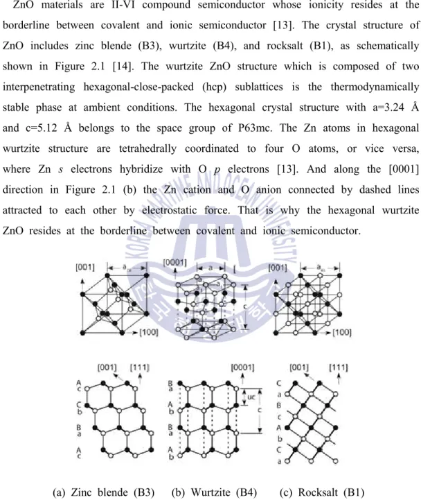
Since the ionic radius of Mg2+ (0.57 Å) is close to that of Zn2+ (0.6 Å), the replacement of Zn by Mg should not cause a significant change of the lattice constant. The compositionally tuned MgxZn1-xO band gap and the corresponding phases are shown in Figure 2.3. The band gap of MgxZn1-xO can be tuned from 3.37 eV to 7.8 eV by controlling the Mg content.
Much of the pn diode analysis can be applied directly to the MS diode with only minor modifications. In 1938, Schottky suggested that the rectification behavior could arise from a potential barrier due to the stable space charges in the semiconductor [33]. 2.2) where ΦB is the height of the Schottky barrier, A is the area of the diode and A* is the effective Richardson constant.
This predicts that for an n-type semiconductor, where ΦB is the Schottky barrier height (SBH) of an "ideal" homogeneous contact, Φm is the work function of the metal and the electron affinity of the semiconductor. Equation (2.1) can be rewritten by taking the logarithms of both sides of the equation.
![Table 2.1 [17] shows the physical properties of ZnO. These properties make it to be an exciting new material in solid state electronics field.](https://thumb-ap.123doks.com/thumbv2/123dokinfo/10555837.0/16.772.103.703.422.967/table-shows-physical-properties-properties-exciting-material-electronics.webp)
Experiment and analysis methods
Experiment methods
- Theory of RF magnetron sputter system
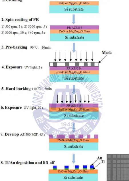
- Fabrication of Ti/Au electrode on ZnO and Mg x Zn 1-x O films
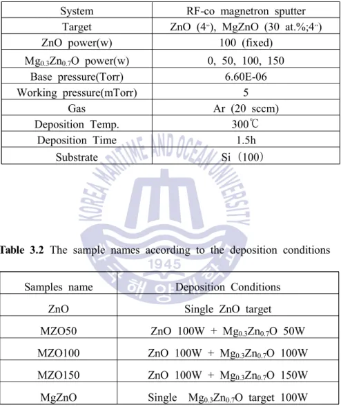
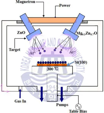
MgxZn1-xO ternary thin films were deposited on n-Si (100) substrates by RF magnetron co-sputtering as shown in Figure 3.1. Before loading into the sputtering chamber, the Si substrates were cleaned with acetone, methanol and deionized water in an ultrasonic apparatus for 15 minutes. Argon gas was introduced at a flow rate of 20 cm3/min, which was controlled using a mass flow controller.
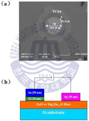
The sample deposited using single ZnO (100W) and Mg0.3Zn0.7O (100W) is referred to as ZnO and MgZnO, respectively. The Ti (10 nm)/Au (50 nm) contact was deposited using the e-beam evaporation system in Figure 3.2, and then the patterning was finally completed by the lift-off method.
Analysis methods
- X-ray diffraction
- Atomic force microscope
- Energy-dispersive X-ray spectroscopy
- Hall effect measurement
AFM has much broader potential and application as it can be used to image any conductive or non-conductive surface. AFM works by bringing a cantilever tip into contact with the surface to be imaged, as shown in Figure 3.5. An ionic repulsive force from the surface applied to the tip deflects the cantilever upward.
The amount of deflection, measured by a laser spot reflected on a split photo detector, can be used to calculate the force. By keeping the force constant while scanning the tip along the surface, the vertical movement of the tip follows the surface profile and is recorded as the surface topography by the AFM. Energy-dispersive X-ray spectroscopy (EDS, EDX, or XEDS), sometimes called energy-dispersive X-ray analysis (EDXA) or energy-dispersive X-ray microanalysis (EDXMA), is an analytical technique used for elemental analysis or chemical. characterization of a sample.
The interaction of an electron beam with a sample target produces a variety of emissions, including X-rays as shown in Figure 3.6. An EDS detector is used to separate the characteristic X-rays of different elements into an energy spectrum, and EDS system software is used to analyze the energy spectrum in order to determine the abundance of specific elements. EDS can be used to find the chemical composition of materials down to a spot size of a few microns and to create elemental composition maps over a much wider raster area.
The HP 4145B Semiconductor Parameter Analyzer is an extremely useful tool for characterizing semiconductor devices when used with LabVIEW. These two parts apply a voltage to the semiconductor device and read the measured current to send back to the LabVIEW. It is based on the van der Pauw technique, a combination of resistance measurement and Hall measurement.
The basic physical principle underlying the Hall effect is the Lorentz force, which is a combination of two separate forces: the electric force and the magnetic force, as shown in Figure 3.8 (a). The objective of the Hall measurement in the van der Pauw technique is to determine the density of the sheet metal carrier ns (ns=nd) by measuring the Hall voltage VH according to Eq. 3.2), where I is the current, B is the magnetic field, d is the thickness of the sample and q is the elementary charge.
Results and discussions
- Results and discussions
- The structural properties of Mg x Zn 1-x O films
- The electrical properties of Mg x Zn 1-x O films
- Conclusions
- The effect of Mg content on electrical properties of Mg x Zn 1-x O films
- Motivation
- Experimental detail
- Results and discussions
- Conclusions
- Schottky diodes prepared with Ag, Au, and Pd contacts on Mg 0.18 Zn 0.82 O films · 55
- Conclusions
Recently, MgxZn1-xO-based Schottky diodes have attracted much attention in UV PD and PV applications [26, 27]. To expand the application of MgxZn1-xO film in deep-UV optoelectronic devices, both high-quality MgxZn1-xO film and good electrical conductivity of the metal/MgxZn1-xO Schottky contact are required. In this work, we present the Schottky contact properties of Ag metal on MgxZn1-xO (0≤x≤0.18) thin films as a function of Mg content without surface treatment.
The MgxZn1-xO films were deposited by RF magnetron co-sputtering with ZnO and Mg0.3Zn0.7O targets. The ternary MgxZn1-xO thin films were deposited on n-Si (100) substrates by RF co-sputtering. 4.8 (a) SEM image showing a top view of the lateral Schottky diode pattern and (b) a schematic cross-section of the Schottky diode.
So the Mg content of the MgxZn1-xO film increases as the RF power of the Mg0.3Zn0.7O target increases. The inset figure shows the I-V characteristics between Ti-Au contacts in MgxZn1-xO thin films, which verifies the good properties of the ohmic contact. So, the barrier height of Ag/MgxZn1-xO Schottky diode increases with increasing Mg concentration.
The increased special contact resistance and resistivity of MgxZn1-xO films is the main point why the series resistance of Schottky devices increases with the increase of Mg concentration. The Ag Schottky diodes based on MgxZn1-xO thin films with the Mg content varying from 0 to 18 at.% are presented in the research. The electrical properties of Schottky diode based on Mg0.18Zn0.82O thin film with Ag, Au and Pd Schottky electrodes are summarized as Table 4.2.
However, in our case, both Pd and Au contacts in the Mg0.18Zn0.82O films show good Schottky properties, which indicate that the MgxZn1-xO films exhibit relatively high quality with fewer native defects. Due to the complicated surface quality of ZnO or MgxZn1-xO films, the Schottky barrier height between the metal and ZnO or MgxZn1-xO is independent of. So the Schottky diode based on Ag metal Mg0.18Zn0.82O film is promising for future application in UV optoelectronic devices.
The Ag, Au and Pd Schottky diodes based on Mg0.18Zn0.82O thin films are presented in this research. The Mg0.18Zn0.82O film-based Schottky diode with Ag metal is promising for future application in UV optoelectronic devices.
Summary & Conclusion
Jang, “Electrical properties of MgxZn1-xO thin films deposited by RF co-sputtering,” 7th International Symposium on Advanced Plasma Science and Its Applications for Nitrides and Nanomaterials, Nagoya, Japan, March 26-31 (2015). Jang, “The Study of Ohmic Contact Properties to MgxZn1-xO alloy films deposited by RF co-sputtering,” 14th International Union of Materials Research Societies-International Conference on Advanced Materials, Jeju Korea October 25-29 (2015). Lee, “A Study on Thin Film Transistors Using MgZnO/ZnO Bilayer as Active Layer,” 15th International Union of Materials Research Societies-International Conference on Advanced Materials, Fukuoka, Japan, August 24-30 (2014).
![Fig. 2.2 The structural models of hexagonal (a) and cubic (b) MgZnO alloys [7]](https://thumb-ap.123doks.com/thumbv2/123dokinfo/10555837.0/18.772.265.530.390.638/fig-2-structural-models-hexagonal-cubic-mgzno-alloys.webp)
![Fig. 2.3 Composition tuned Mg x Zn 1-x O band gap and the corresponding phases [24]](https://thumb-ap.123doks.com/thumbv2/123dokinfo/10555837.0/19.772.205.566.424.748/fig-composition-tuned-mg-zn-band-corresponding-phases.webp)
![Fig. 2.4 Absorption spectra for Mg x Zn 1-x O thin films at room temperature [23]](https://thumb-ap.123doks.com/thumbv2/123dokinfo/10555837.0/20.772.204.622.340.632/fig-absorption-spectra-mg-zn-films-room-temperature.webp)
![Fig. 2.5 Energy band diagrams for Schottky diode based on n-type semiconductor under (a) flat band (equilibrium), (b) forward bias (V a >0), and (c) forward bias (V a <0) conditions [33]](https://thumb-ap.123doks.com/thumbv2/123dokinfo/10555837.0/24.772.83.690.404.669/energy-diagrams-schottky-semiconductor-equilibrium-forward-forward-conditions.webp)