Vol. 23, No. 3 (2013)
177
Effect of Fabricating Nanopatterns on GaN-Based
Light Emitting Diodes by a New Way of Nanosphere Lithography
Fatima Tuz Johra and Woo-Gwang Jung †
School of Advanced Materials Engineering, Kookmin University, Seoul 136-702, Korea (Received November 21, 2012 : Received in revised form January 3, 2013 : Accepted January 10, 2013)
Abstract
Nanosphere lithography is an inexpensive, simple, high-throughput nanofabrication process. NSL can be done in different ways, such as drop coating, spin coating or by means of tilted evaporation. Nitride-based light-emitting diodes (LEDs) are applied in different places, such as liquid crystal displays and traffic signals. The characteristics of gallium nitride (GaN)- based LEDs can be enhanced by fabricating nanopatterns on the top surface of the LEDs. In this work, we created differently sized (420, 320 and 140 nm) nanopatterns on the upper surfaces of GaN-based LEDs using a modified nanosphere lithography technique. This technique is quite different from conventional NSL. The characterization of the patterned GaN-based LEDs revealed a dependence on the size of the holes in the pattern created on the LED surface. The depths of the patterns were 80 nm as confirmed by AFM. Both the photoluminescence and electroluminescence intensities of the patterned LEDs were found to increase with an increase in the size of holes in the pattern. The light output power of the 420-nm hole-patterned LED was 1.16 times higher than that of a conventional LED. Moreover, the current-voltage characteristics were improved with the fabrication of differently sized patterns over the LED surface using the proposed nanosphere lithography method.Key words
nanosphere lithography, light emitting diode, nanopatterning, photoluminescence, current-voltage characteristics.
1. Introduction
Nanopattern fabrication techniques are widely explored in recent years as the demand for smaller and more efficient materials are increasing for use in applications such as solar cells,
1)light emitting diodes,
2,3)enhanced Raman scattering,
4)biosensors,
5)and bioreactors.
6)Currently, there are many methods available for nanopattern fabri- cation, especially various kinds of lithography techniques.
Photolithography is the most commonly used technique for patterning, but it is not useful for nanopatterning. Nano- imprint lithography can be used for nanopatterning, but this technique is expensive. Electron beam and x-ray lithography have also been used; however, even they have some drawbacks.
Nanosphere lithography(NSL) is a widely used technique for the patterning of substrates. It involves placing nano- spheres in a tightly packed pattern on a substrate in order to create a mask for pattern transfer.
7)After deposition of thin film and removal of nanosphere, the nanopattern can be achieved. This technique uses various types of methods
such as drop coating, spin coating, and tilted evaporation.
The wide bandgap of gallium nitride(GaN, 3.4 eV) makes it one of the most promising materials in opto- electronics, especially in the fabrication of light emitting diodes(LEDs). Improving the light extraction efficiency of LEDs has become a topic of considerable interest. The incorporation of micro- and nanoscale features of various geometries such as disc, ring, and hexagon into GaN LEDs have previously been reported to promote the light extraction efficiency of the LEDs.
8,9)The light output efficiency of GaN-based UV/visible LEDs, however, con- tinue to be low compared to that of conventional light sources used in high-flux lighting systems.
10)In this work, a new process of monolayer formation has been designed using nanosphere lithography. We applied this technique successfully to fabricate surface patterns with three different sized holes on GaN-based LED samples using polystyrene nanospheres. Our aim was to enhance the characteristics of GaN-based LEDs through surface patterning. Both the monolayer and nanopatterns were investigated using scanning electron microscope. The
†
Corresponding author
E-Mail : [email protected] (W.-G. Jung, Kookmin Univ.)
© Materials Research Society of Korea, All rights reserved.
This is an Open-Access article distributed under the terms of the Creative Commons Attribution Non-Commercial License (http://creative-
commons.org/licenses/by-nc/3.0) which permits unrestricted non-commercial use, distribution, and reproduction in any medium, provided the
original work is properly cited.
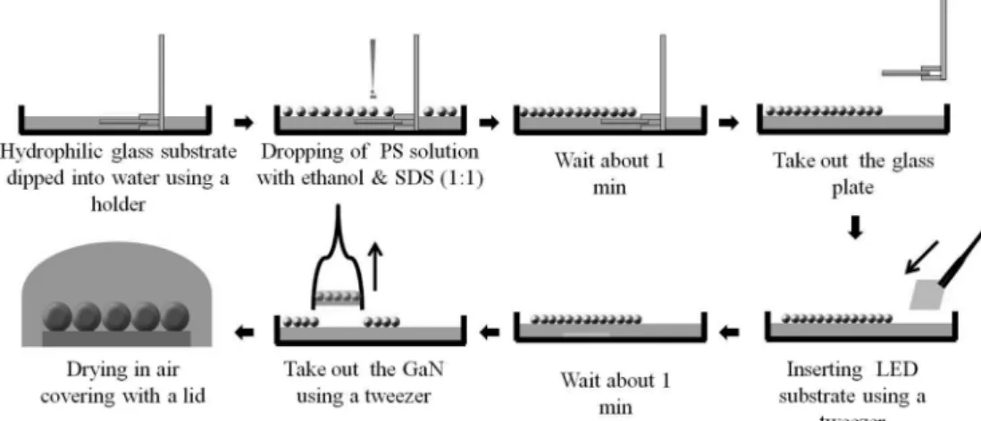
A 1:1 mixture of PS(720 nm) suspension and ethanol/
SDS(400:1) was used to prepare a close-packed PS monolayer. After pouring DI water into a petri dish, a glass substrate(Piranha cleaned to make the surface hy- drophilic) was placed into the dish with the help of a holder. Approximately 30 µL of the PS solution was dropped onto the glass substrate and kept for few minutes to form self-assembled PS monolayers, floating on the water surface. Following this, the main substrate(any kind of substrate with a hydrophilic surface), on which the monolayer is to be transferred, was dipped into the water and the substrate with monolayer was taken out using tweezers. The substrate was then dried in air after covering it with a lid. The schematic diagram of this process is shown in Fig. 1.
Monolayers were formed and transferred onto the sur- face of LED substrates(1 × 1 cm, RCA cleaned to make the surface hydrophilic) using the technique mentioned above.
After the PS monolayer transfer, the LED substrates were heated to 80
oC, and then subjected to Reactive Ion Etching(RIE) to produce patterns of different sizes. RIE ashing was carried out under a 10 sccm O
2flow rate, 150 mTorr working pressure, and 100 W plasma power for 3, 5, and 7 min to obtain different sized nanospheres as well as a hard mask. A sphere mask of appropriate size can be easily produced by controlling the ashing time.
10)chamber pressure of 5 mTorr with an etching depth of 85 nm.
After etching, the Ni mask was then removed using an appropriate etchant and its PL characteristics were mea- sured. In order to expose the n-GaN surface of LED, etching was performed under inductively coupled Cl
2/ CH
4/H
2/Ar plasma with flow rates of 30/8/8/16 sccm. Ni/
Au as a p-ohmic metal and Ti/Al as an n-ohmic metal was fabricated on top of LEDs after thermal annealing at 650
oC for 5 min to activate the p-type dopants. Metal electrodes were deposited on selected areas by e-beam evaporation.
Field-emission scanning electron microscopy(FE-SEM) images and energy dispersive x-ray spectrometry(EDS) analyses were performed on a JEOL JSM5410 scanning electron microscope. After patterning the surfaces of GaN- based LEDs, the current-voltage(I-V) characteristics were measured with a semiconductor parameter analyzer(Agilent 4155C). The light output power vs. current(L-I) charac- teristics were measured by a LEOS-150 probe system (Withlight Co. Ltd. Korea), and the local electrolumines- cence was characterized by charging the current injection with 20 mA. The PL was mapped using an Accent RPM 2000 system coupled with an Nd-YAG laser as the excit- ation light source at room temperature.
Fig. 1. A Schematic diagram of the formation of a monolayer on GaN substrate.
3. Results and Discussion
A new nanosphere lithography process was implemented in this study as a new way of forming surface mono- layers. Here, the PS suspension was hydrophilic in nature.
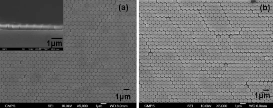
If the substrate was hydrophobic, it would be difficult to get uniform and crack-free monolayer on the substrate. In this new process, we employed glass substrates as it is easy to make the glass surface hydrophilic by treating with piranha solution. When the PS suspension was dropped onto the glass substrate which immersed in water, both the surface tension of water and glass help to form monolayers on the surface of the water. Fig . 2 shows the
PS monolayer transferred onto a hydrophilic glass substrate and onto a GaN-based LED surface.
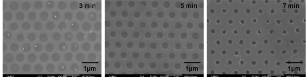
To enhance the characteristics of GaN-based LEDs, the surface of these substrates was patterned. Fig . 3 shows the FE-SEM images of shrunken PS monolayer coated on top of GaN-based LED. The sphere diameter, which was initially 720 nm, changed to 540, 400, or 200 nm depending on the ashing time. Before ashing, all of the samples were heated at 80
oC. This is because, during ashing time, the PS beads may not remain at a fixed place.
To ensure a fixed position for the PS beads,
12)it was heated for a short time so that the PS beads melted a little and attached to the substrate. As a result, the arrangement Fig. 2. A polystyrene monolayer transferred onto a substrate; (a) glass, (b) LED surface.
Fig. 3. A PS surface monolayer after ICP ashing and the relationship between the PS diameters and the ashing time.
of the PS beads remained unchanged, which helped to create the regular PS patterns without any displacement.
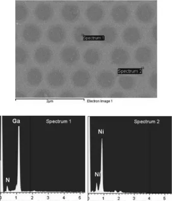
Ni metal patterned onto LED substrates after PS removal is shown in Fig. 4. The size became smaller than the PS beads; 540, 400 and 200 nm tends to 420, 320 and 140 nm respectively. It is dependent on the thickness of the metal mask. The hole pattern depth was approximately 85 nm, which was confirmed by both FE-SEM and AFM (Fig. 5). Fig . 6 also confirms the removal of PS beads from the surface of the substrates.
In order to evaluate the light extraction characteristics of the patterned GaN-based LED, PL of the as-prepared patterned LEDs were compared with that of conventional LEDs. From Fig. 7, it is easily observed that the LED with the largest hole size exhibited the highest PL intensity.
The value was found to be almost two times higher than
that of the conventional LED. The PL intensity was also found to increase with an increase in the size of the hole as well as with a decrease in the distance between two holes. This may be due to the fact that, in certain regions, the number of holes remains the same, but because of changes in the size, the light reflections then increased with the increasing size of the holes. It also can be explain in terms of photonic crystal.
The electroluminescence characteristics of the 420-nm patterned LED were also compared with those of the conventional LED. Fig . 8 shows that the electrolumines- cence intensity of the 420-nm patterned GaN-based LED is higher compared to that of the conventional LED. This is because the refractive indices change periodically, and thus, the total internal reflection was suppressed at the GaN surface.
Fig. 5. A patterned LED substrate; (a) SEM image and (b) AFM image.
Fig . 9 compares the I-V characteristics of the patterned LED with those of the conventional LED. The forward voltages for 470-, 370-, 140-nm patterned LEDs and the conventional LED were measured at injection currents of 20 mA and were found to be 4.96, 5.12, 6.02, and 5.77 V, respectively. The forward voltages of the patterned LEDs, except the one with smallest holes(140 nm), were smaller than that of the conventional LED, which refers to an improvement in the ohmic contact resistance caused by an increase in the contact area. In the case of the 140-nm patterned LED, some amount of defects were found,
which may be responsible for the poor I-V characteristic compared to the others.
Fig . 10 shows a comparison between the light output Fig. 8. Comparison of electroluminescence intensities of patterned LEDs and conventional LED.
Fig. 9. I-V characteristics of the patterned LEDs and conventional LED.
Fig. 10. L-I characteristics of the patterned LEDs and conventional LED.
Fig. 6. EDS images of the Ni metal mask after PS monolayer removal.
Fig. 7. Comparison of photoluminescence intensities of patterned
LEDs and conventional LED.
useful to make large scale of monolayer. Here a variety of sizes and patterns can be achieved using this easier and more economical method. With this technique, different sized patterns were fabricated on GaN-based LED surfaces, which enhanced the performances of the LEDs compared to those of conventional LEDs. This may probably due to the increase in light escape probability in the patterned LEDs.
Acknowledgments
This study was supported by the ERC(Center for Ma- terials and Processes of Self Assembly) program of MOST/KOSEF(R11-2005-048-00000-0) and the Basic Sci- ence Research Program through the National Research Foundation of Korea(NRF) funded by the Ministry of Education, Science and Technology(KRF-2011-0024104).
2, 2103 (2008).
7. C. L. Haynes and R. P. Van Duyne, J. Phys. Chem. B, 105, 5599 (2001).
8. H. W. Choi, C. W. Jeon, M. D. Dawson, P. R. Edwards and R. W. Martin, IEEE Photon. Tech. Lett., 15, 510 (2003).
9. H. W. Choi, C. W. Jeon, C. Liu, I. M. Watson, M. D.
Dawson, P. R. Edwards, R. W. Martin, S. Tripathy and S.
J. Chua, Appl. Phys. Lett., 86, 021101 (2005).
10. C. Huh, J. M. Lee, D. J. Kim, and S. J. Park, J. Appl.
Phys., 92, 2248 (2002).
11. Y. Lee, M. Alam, J. Y. Kim, W. G. Jung and S. D. Kim, Kor. J. Mater. Res., 20, 550 (2010) (in Korean).
12. C. Cong, W. C. Junus, Z. Shen and T. Yu, Nanoscale Res.
Lett., 4, 1324 (2009).