New Physics: Sae Mulli,
Vol. 69, No. 2, February 2019, pp. 124∼127 http://dx.doi.org/10.3938/NPSM.69.124
Crystal Properties of TiO
2Thin Films Grown at Low Temperatures by Reactive DC Magnetron Sputtering
Hyeok Jee · Jin-Soo Kim
Department of Physics, Jeju National University, Jeju 63243, Korea
Hye-Won Seo
∗Department of Physics, Jeju National University, Jeju 63243, Korea and Jeju National University Research Institute for Basic Science, Jeju 63243, Korea (Received 11 September 2018 : revised 29 October 2018 : accepted 29 October 2018)
We grow anatase-TiO2 thin films in the low-temperature range from room temperature (RT) to 300 ◦C by using a reactive DC magnetron sputtering method. In particular, we focused on the dependences of the crystalline properties of TiO2 thin films on the growth temperature. The crystallite size and population were found to increase with increasing temperature, which was revealed by using X-ray diffraction and Raman spectroscopic methods. Using a comparative study based on atomic force microscopy, we also identified that the crystallites in the TiO2thin films were of high quality.
PACS numbers: 61.43.-j, 68.55.-a, 81.15.Cd
Keywords: TiO2, Crystallites, Growth temperature, Thin films
I. INTRODUCTION
Since Fujishima found the photo-electrochemical water-splitting properties of titanium dioxides (TiO2) under the UV illuminations, its adaption to photo- voltaics, photocatalyst, and sensor devices have been ac- tively pursued [1–3]. This intensive study leads to the commercial applications in the related fields [4]. The feasibility of fabrication process and the low cost fabri- cation becomes more important for enabling the practi- cal utilizations. Recently, flexible electronics including electro-optical devices and bio-sensors have gotten spe- cial attentions as a next generation platform [5,6]. To realize TiO2as an element of flexible devices, the growth needs to be controlled below a certain temperature. The polyethylene terephthalate or polyethylene naphthalate plastic insulating films, which are typically used for the conductive template or substrate for the flexible electron- ics, becomes resistive and thermally-deformative beyond 200 ◦C [7].
∗E-mail: [email protected]
A few groups have reported the physical vapour depo- sitions of TiO2films, such as sputtering and atomic-layer deposition, at the low temperature regions [8–10]. How- ever, their focus was limited mainly to the anatase-rutile phase transitions dependent on the growth temperature or its effects on the photo-catalytic performances. Note that the grain size and the related defects of films are also a crucial factor need to be considered. Especially, it is known that there is an optimal crystal or gain size to have the enhanced catalytic properties [11,12].
With this in mind, we paid attention to the low tem- perature growth of TiO2films by reactive DC sputtering methods. We then studied the structural properties of the as grown TiO2films, in terms of crystallite qualities and sizes.
II. EXPERIMENTAL METHODS
We have grown TiO2 thin films with 1 × 1 inch on glass substrate using a reactive DC magnetron sputter- ing. Target material used was pure titanium disk with 2
This is an Open Access article distributed under the terms of the Creative Commons Attribution Non-Commercial License (http://creativecommons.org/licenses/by-nc/3.0) which permits unrestricted non-commercial use, distribution, and reproduction in any medium, provided the original work is properly cited.
Crystal Properties of TiO2 Thin Films Grown at Low Temperatures by Reactive DC Magnetron· · · – Hyeok Jee et al. 125
inches in diameter. Distance of target and substrate was maintained at 50 mm. Argon of 10 sccm and oxygen of 2 sccm were used as sputtering and reactive gas, respec- tively. The process pressure was kept at ∼4.6 × 10⁻³ Torr. Plasma power of 150 W was used. The substrate temperature was changed from the room temperature (RT), 100, 200, to 300 ◦C.
After injection of argon gas, the plasma between the target and substrate was shielded by a shutter, and the pre-sputtering was performed. After the temperature was raised to the growth temperature and the target discharge impedance was stabilized, oxygen gas was in- jected. The shutter was then removed and the deposition was carried out for 10 minutes. The films were quenched to the RT after the deposition.
We monitored the crystal properties of the thin films using X-ray diffraction (XRD) (Empyrean, PANalytical) with CuKα radiation (λ = 1.5406 Å), and using the Ra- man spectroscopy (LabRAM HR Evolution, HORIBA) with Ar+ laser (λ = 514 nm). The Atomic force mi- croscopy (Bruker, Multimode 8 AFM V) was used to scan the 0.5 × 0.5 µm range to verify morphology and roughness of the films. The thickness of thin film was measured with a Thin Film Thickness Measurement Sys- tem (ST4000, K-MAC).
III. RESULTS
Fig. 1(a) shows the Raman spectra obtained from the films grown with a different temperature from RT to 300
◦C. The Raman peaks were observed at 143.5, 396.5, 517.9 and 639.0 cm−1, which correspond to the five modes (1A1g+ 2B1g+ 2Eg) of anatase TiO2 [13]. The peaks at 143.5 and 639.0 cm−1 are attributed to 2Eg (υ1, υ5) mode while the peak at 396.5 cm−1is originated from B1g(υ2) mode. The peak at 517.9 cm−1are known to be combined A1g(υ3) + B1g(υ4) modes [14], which is difficult to distinguish at room temperature but can be separated at a low temperature, ∼73 K [15]. Note that A1g(υ3), B1g(υ4) and Eg(υ5) are classified as stretching mode and, Eg(υ1) and B1g(υ2) are bending mode.
As the substrate temperature increases from RT to 300
◦C, it was observed that the intensity of 143.5 cm−1, Eg(υ1), increases by 5.5 times, which reveals the im- proved crystal qualities and populations. Its full-width
Fig. 1. (Color online) (a) Raman spectra of TiO2 films grown at RT to 300◦C and (b) Raman intensity (black points) and FWHM (blue points) of the peak at 143.5 cm−1 (Eg).
at half maximum (FWHM) decreases from 12.63 to 11.62 cm−1, when the temperature is elevated to 200 ◦C, and increases again up to 12.1 cm−1 at 300◦C, as shown in Fig. 1(b). The FWHM and shift of Eg(υ1) peak are usu- ally used to estimate the crystallite size, typically smaller than 20 nm, based on the phonon confinement effect [16].
But, any clear change both in FWHM and peak position were not observed, which is possibly due to no difference in crystallite size or overall bigger size of crystallites (>
20 nm).
To understand the crystallographic properties of the films dependent on the growth temperature, the XRD was investigated, as shown Fig. 2(a). In comparison, Fig. 2(b) shows the XRD results of the 200 and 300◦C films in log scale, which were measured in a longer time scale,×2.
As the temperature increases from RT to 300 ◦C, the XRD peak at 2θ = 25.34◦, anatase (101), becomes stronger, which agrees with the Raman results showing
126 New Physics: Sae Mulli, Vol. 69, No. 2, February 2019
Fig. 2. (Color online) (a) XRD of TiO2 films grown at RT to 300 ◦C, (b) XRD of TiO2 films of 200 and 300◦C in a log scale, and (c) XRD intensity (black points) and FWHM (blue points) of the peak at anatase (101) vs. growth temperature.
Fig. 3. (Color online) AFM images of TiO2 films (0.5× 0.5 µm); (a) RT, (b) 100◦C, (c) 200◦C, and (d) 300◦C.
the gradual improvement of crystal qualities. The poly- crystalline properties were also revealed. As growth tem- perature increases, the other 2θ peaks at 48.1◦, 54.0◦, and 55.1◦ were also observed, which are anatase phase of (200), (105), and (211).
Fig. 2(c) presents the intensity and FWHM of the peak (101) of 2θ = 25.34◦ vs. growth temperature. The aver- age crystallite size was calculated from FWHM based on the Scherrer formula, D = β cos θkλ , where k is a dimen- sionless shape factor which is equal to 0.9, λ is the wave- length of CuKα radiation, 0.15418 nm, β is FWHM, and θ is the diffraction angle. The crystallites size was found to be 25.1 nm (100 ◦C), 25.7 nm (200◦C) and 31.6 nm (300 ◦C). The higher growth temperature leads to the bigger crystallite size, which is also inverse of the (101) peak intensity. The substrate heating enhances the sur- face migration of atoms and causes the better crystal qualities and the bigger size.
However, the XRD broadening can be caused not only by crystallite size effect but also by stain or strain-
Table 1. AFM results of TiO2 films grown at RT to 300
◦C.
RMS roughness Crystallite size (nm)
(nm) Grain I Gain II
RT 1.8 21.8 10.6
100◦C 2.11 22.7 12.5
200◦C 2.23 25.0 13.0
300◦C 2.58 28.2 13.9
induced defects. To get an insight of this issue, we used the AFM methods and identified the physical crystallite size. The Fig. 3 shows the AFM scanning images of 0.5
× 0.5 µm. As the substrate temperature increased, the root-mean-square (RMS) roughness value increased from 1.8, 2.11, 2.23 to 2.58 nm (Table 1). Here, we categorize the crystallites into two groups; grain I (bright in images and bigger) and grain II (dark in images and smaller).
We believe that the grain I is formed by the coagulation or Oswald-ripening of the grain II. The size of grain I increases from 21.8 to 28.2 nm when the growth tem-
Crystal Properties of TiO2 Thin Films Grown at Low Temperatures by Reactive DC Magnetron· · · – Hyeok Jee et al. 127
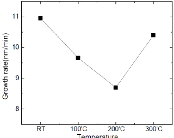
Fig. 4. Growth rate of TiO2 films vs. growth tempera- ture.
perature is escalated from RT to 300 ◦C, which are very similar to the results obtained from Scherrer’s formula.
In other words, the grain I are of good crystal qualities but the grain II may have poor crystal properties which may not attribute to the XRD peaks. In turns, this re- sult confirmed that crystallites of grain I have negligible strain or defects.
We also studied the growth rate of the films (Fig. 4).
As the growth temperature increases to 200 ◦C, the growth rate decreases from 11.0 to 8.7 nm/min while the growth rate jumps to 10.4 nm/min at 300◦C. Here, we adapt the model of solid-state glass to crystallization [17], which is reasonable because 1) the melting temper- ature of Ti is quite high and 2) TiO2films grown at a low temperature are mainly amorphous. Temperature of the nucleation is typically lower than that of crystal growth [17], which can explain the growth rate having the mini- mum at the medium temperature, neither the highest or the lowest. In other words, the 200◦C is located beyond the nucleation temperature but below the crystallization temperature.
IV. CONCLUSION
We have grown rutile-TiO2 films at the low tempera- ture regions from RT to 300◦C using reactive DC mag- netron sputtering methods. Based on the comparative study of XRD and AFM results, we found that 1) the size of crystallites grows become bigger from 25.1 to 31.6 nm as the growth temperature increases from 100 to 300◦C and 2) they have negligible strain or defects. The growth temperature of 200 ◦C is expected to be between the
nucleation and the crystallization temperature of rutile- TiO2films.
ACKNOWLEDGEMENTS
This work was supported by the 2018 scientific pro- motion program funded by Jeju National University.
REFERENCES
[1] A. Fujishima and K. Honda, Nature 238, 37 (1972).
[2] A. Hagfeldt and M. Graetzel, Chem. Rev. 95, 49 (1995).
[3] A. L. Linsebigler, G. Lu and J.T. Yates, Jr., Chem.
Rev. 95, 735 (1955).
[4] T. Ochiai and A. Fujishima, J. Photoch. Phoyobio.
C 13, 247 (2012).
[5] S. R. Forrest, Nature 428, 911 (2004).
[6] F. J. Pavinatto, C. W. A. Paschoal and A. C. Arias, Biosens. Bioelectron. 67, 553 (2015).
[7] V. Zardetto, T. M. Brown and A. Di Carlo, J.
Polym. Sci. B Polym. Phys. 49, 638 (2011).
[8] V. Senthilkumr, M. Jayachandran and C. Sanjeevi- raja, Thin Solid Films 519, 991 (2010).
[9] K Safeen, V. micheli, R. Bartali, G. Gottardi and N. Laidani, J. Phys. D: Appl. Phys. 48, 295201 (2015).
[10] H. E. Cheng, C.-M. Hsu and Y.-C. Chen, J. Elec- trochem. Soc. 156, D275 (2009).
[11] N. Xu, Z. Shi, Y. Fan, J. Dong and J. Shi et al., Ind. Eng. Chem. Res. 38, 373 (1999).
[12] A. J. Maira, K. L. Yeung, C. Y. Lee, P. L. Yue and C. K. Chan, J. Catal. 192, 185 (2000).
[13] G. D. Venkatasubbu, V. Ramakrishnan, V.
Sasirekha, S. Ramasmy and J. Kumar, J. Exp.
Nanosci. 9, 661 (2014).
[14] T. Ohsaka, F. Izumi and Y. Fujiki, J. Raman Spec- trosc. 7, 321 (1978).
[15] U. Balachandran and N. G. Eror, J. Solid State Chem. 42, 276 (1982).
[16] S. Balaji, Y. Djaoued and J. Robichaud, J. Raman spectrosc. 37, 1416 (2006).
[17] D. Savytskii, B. Knorr, V. Dierolf and H. Jain, Sci.
Rep. 6, 23324 (2016).