A Methodology of Dual Gate MOSFET Dosimeter with Compensated Temperature
Sensitivity
Young Hwan Lho
*★Abstract
MOS (Metal-Oxide Semconductor) devices among the most sensistive of all semiconductors to radiation, in particular ionizing radiation, showing much change even after a relatively low dose.
The necessity of a radiation dosimeter robust enough for the working environment has increased in the fields of aerospace, radio-therapy, atomic power plant facilities, and other places where radiation exists. The power MOSFET (Metal-Oxide Semiconductor Field-Effect Transistor) has been tested for use as a gamma radiation dosimeter by measuring the variation of threshold voltage based on the quantity of dose, and a maximum total dose of 30 krad exposed to a 60Co
-radiation source, which is sensitive to environment parameters such as temperature. The gate oxide structures give the main influence on the changes in the electrical characteristics affected by irradiation. The variation of threshold voltage on the operating temperature has caused errors, and needs calibration. These effects can be overcome by adjusting gate oxide thickness and implanting impurity at the surface of well region in MOSFET.Key words: Dosimeter, MOSFET,
irradiation, threshold voltage, dose* Dept. of Railroad Electricity and Information Communication, Woosong University
★Corresponding author
※ Acknowledgment The project was conducted under the Space R&D program by Ministry of Education, Science and Technology (MEST) of Korea
Manuscript received June. 2, 2011; reviced June. 29, 2011
I. Introduction
Recently, diode detectors and MOSFET radiation dosimeters have found a wide range of applications in the fields of aerospace, medicine, atomic power, and personal dosimetry. The study to perform and detect energy dispersive spectroscopy of high energy radiation such as -rays, -rays, and other uncharged and charged particles have done intensively in recent years. While irradiation usually
leads to the creation of structural defects, Ionising radiation has been found to be widely applicable in modifying the structure and properties at the surface of diode and MOSFET.
A diode detector is a p-n junction diode. The diodes are produced by taking n type or p type silicon and counter-doping the surface to produce the opposite type material. Radiation makes electron-hole pairs in the body of the dosimeter, including the depletion layer. Diodes show a variation in dose response with temperature, and dependence of signal on the dose rate. Diodes are used in the short circuit mode, since the mode shows a linear relationship between the measured charge and dose. A diode detector has the advantage of measuring in real time within a
limited distance between the radiation source and the irradiated surface.
A MOSFET, a miniature silicon tranisitor, has the electrical characterisitcs of excellent spatial resolution and very little attenuation of the beam due to its small zize.
While radiation-sensing MOSFETs generally require very thick gate oxides and should be manufactured using expensive custom processes, appropriately designed floating gate dosimeters [1, 2]
can be fabricated with almost any commercial CMOS technology providing two poly-silicon layers.
In the devices, full sensitivity is obtained although no bias is applied during irradiation. This is resulted from the built-in electric field in the oxide layers of the device made by the charge stored on the floating gate. Ionizing radiation often causes detrimental effects on the characteristics of MOS devices and circuits. The threshold voltages, and leakage currents of transistors change as a function of a number of factors: the temperature during irradiation, the total dose of radiation affected and its energy, the bias applied during the irradiation, and the dose rate at which the radiation is emitted.
MOSFET radiation dosimeters are less affected by dose rate than diode detectors, and they have constant sensitivity even after accumulated doses. In this method, threshold voltage() decreases linearly as the variation of temperature in the range of 25 ℃ to 45 ℃ [3]. A simple method for estimating the threshold voltage shift due to ionizing irradiation at low dose rate was recently proposed for power MOSFETs [4]. This method consists of estimating the threshold voltage shift by the oxide charge trapping at the gate oxide immediately after irradiation.
In order to measure the radiation response, the MOSFET characteristics were measured [3]. In particular, the drain current, , as a function of the gate voltage, , was obtained for each transistor under pre-irradiation and post-irradiation conditions.
The drain current in the saturation region is written as
(1.1)
where is the trans-conductance [5], and
is gate voltage.The equation in the linear region is given by
(1.2)
where is the drain voltage.
II. Design of Module
MOSFET dosimeters are based on the measurement of the threshold voltage, which is a linear function of the absorbed dose. Ionizing radiation penetrating the oxide produces a charge that is permanently trapped, thus causing a change in threshold voltage. The cumulated dose may be measured during or after irradiation. Similarly to diodes, single MOSFETS exhibit a temperature dependence, but this effect can be overcome by specially designed dual MOSFET detector. In general, they show non-linearity of response for more than critical doses which do not keep adequate linearity.
The conventional MOSFET dosimeter consists of two gates with the same oxide gate thickness. This has the inherent problem of measurement error due to variation in temperature. In this paper, a radiation dosimeter with two gates of different oxide thickness is implemented, and a methodology robust to the temperature variation is suggested to measure radiation dose by the difference between the threshold voltages of the two gates.
The gate voltage required to make an inversion layer [6] below the SiO2 is called the threshold voltage and can be represented as
(1.3)
where is the metal-semiconductor work function difference, is the Fermi level, is the depletion charge by inversion, is the charge in the SiO2, and is the capacitance of the SiO2. MOS devices have enough sensitivity to radiation, in particular ionizing radiation, to show a large change even after a relatively low dose. The gate oxide structures give the main influence on the changes in the electrical characteristics affected by irradiation. A change of the I-V characteristics towards more negative values of the gate voltage is brought by a charge trapping at the gate oxide.
This is very serious for n-channel devices when the I-V curve is shifted past zero volts as the current increases sharply. This effect is often considered as a change in gate threshold voltage.
Differentiating Eq. (1.3), we can obtain a relation between the descent rate of threshold voltage ∆
and the change of charge ∆ in SiO2 given by
∆ ∆ (1.4)
where is gate oxide capacitance of MOSFET, and the change of charge, ∆, depends on the dose. The change of threshold voltage is proportional to the change of charge. When radiation
is applied, the slope descent rate of the threshold voltage reduces linearly as the total dose increases.
Here, the descent rate is an increasing function of the threshold voltage.
The charge is influenced by the fixed oxide charge
and the interfacial trap charge as shown in Eq. (1.5).∆ ∆ ∆ (1.5) When the oxide is irradiated, a greater number of dangling bonds are created. The dangling bonds in SiO2 near the interface between Si and SiO2 will trap charge , and this charge is negative for an n-channel MOS because the sign of the voltage of
applied at the gate opposite for a MOSFET.
The fixed charge makes the threshold voltage a more negative value for a MOSFET. The fixed oxide charge is more dominantly affected by radiation than the interfacial trap charge, which is almost the same in different MOSFETs.
In the absence of a work function difference and oxide charge, it is shown that the threshold voltage [7] is given by
(1.6)
where is the silicon dielectric constant, is electron charge, and is peak doping concentration at the channel region of MOSFET.
Differentiating Eq. (1.6) with respect to temperature leads to
(1.7)
The Fermi level [7] changes with temperature because the energy gap varies with temperature.
(1.8)
where is the band gap energy of silicon at the absolute temperature. Note that the threshold voltage will change at a higher rate for thicker gate oxides and higher substrate doping levels.
Fig. 2.1(a) and (b) show the circuits of conventional MOSFET dosimeters [8, 9]. Both MOSFETs have a common source and both drain D1 and D2. The biased voltage is applied to one gate, and the two drains are connected to another gate in Fig. 2.1(a). The structure has more stored charge in the gate attached to the biased voltage than that of the other gate, and the variation of
threshold voltage can be affected by the temperature. Fig. 2.1(b) depicts the two sources as common, and each gate and DC sources of I1 and I2 are connected to drain D1 and D2, respectively.
These kinds of modules can be easily affected by temperature, and cause measurement error.
Fig. 2.1(a) Circuit of a conventional MOSFET dosimeter
Fig. 2.1(b) Schematic of a conventional MOSFET dosimeter
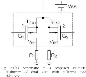
The proposed MOSFET dosimeter structure consisting of dual gates with different oxide thicknesses [10] is shown in Fig. 2.1(c). The threshold voltage shift due to radiation is proportional to the thickness of gate oxide [11]. In fabricating devices, the initial threshold voltages of MOSFET 1 and MOSFET 2 are adjusted to the same value by applying the implantation of peak concentration in the channel region. In controlling the threshold voltage, the Fermi level is determined by the surface impurity density in the area of gate channel [5] as shown in Eq. (2.1).
ln
(2.1)
where is the carrier density of pure silicon semiconductor, is Boltzmann's constant, is the absolute temperature, is the peak density at the surface, and is the electron charge.
Fig. 2.1(c) Schematic of a proposed MOSFET dosimeter of dual gate with different oxide thickness
The ion implantation process in part has been carried out to get the desired threshold voltage. In n-MOSFET, 70 keV ∼ 120 keV energy of BF2
source are applied with a density of 1012 ∼ 1013 particles/cm2 impurity.
III. Methodology of Measurement
The relationship between pre-irradiation and post-irradiation of the two MOSFETs with different gate oxide thickness is shown as × Dose (3.1)
× Dose
(3.2)
where and are threshold voltages at pre-irradiation, and and are proportional constant to dose. Taking the difference of Eq. (3.1) and (3.2), we obtain Eq. (3.3) when the initial threshold voltage of and are equal.
× Dose (3.3)
In order to quantify the radiation response, two kinds of commercial grade IR MOSFETs (100V and 200V of are chosen for testing. The threshold voltage is tested with the specifications irradiated
by source using 60Co up to a maximum total dose of 30 Krad. The test procedure and method is carried out using Mil-Std-883 Method 1029. A sample size of six pieces is used for each test.
Figures 3.1 and 3.2 show the threshold voltage of irradiated MOSFETs based on the quantity of dose.
The total doses are 0, 2.5, 5, 7.5, 10, 20, and 30 krad, respectively, and the dose rate is 4 rad/sec.
As shown in Fig. 3.1 and 3.2, the threshold voltages of the 100 V and 200 V MOSFETs decrease linearly as the quantity of the total dose is increased up to 30 Krad at the same dose rate. The slope of the threshold voltage shown in Fig. 3.1 for the 100 V MOSFET is less steep than that of the 200 V MOSFET shown in Fig. 3.2, which is due to the thickness of the gate oxide.
0 5 10 15 20 25 30
1.6 1.8 2.0 2.2 2.4 2.6 2.8
Vth (v)
Total Dose (k rad)
FET1 FET2 FET3 FET4 FET5 FET6
Fig. 3.1 Threshold voltages of 100 V MOSFETs under a dose rate of 4 rad/sec from 0 to 30 Krad
0 5 10 15 20 25 30
2.4 2.5 2.6 2.7 2.8 2.9 3.0
Vth(V)
Total Dose ( k rad)
FET 1 FET 2 FET 3 FET 4 FET 5 FET 6
Fig. 3.2 Threshold voltages of 200 V MOSFETs under a dose rate of 4 rad/sec form 0 to 30 Krad
When we apply radiation, the slope descent rate of the threshold voltage reduces linearly as the total dose increases. In other words, we observe that the descent rate is an increasing function of the threshold voltage. Here, the difference in threshold
voltage between pre-irradiation and post-irradiation is proportional to the dose as shown in Eq. (3.3).
The initial threshold voltages should be adjusted to equal to determine the dose only by the difference of threshold voltage on the implemented dosimeter.
The threshold voltage of the 100 V MOSFETs with thin oxide thickness decreases from 2.99 V at
to 2.3 V after 30 Krad, and that of the 200 V MOSFETs with a greater oxide thickness varies from 2.86 V to 1.62 V. (3.4)
(3.5) where is the dose.
The linear fitting slope for 100 V MOSFET is 0.016 and that for 200 V MOSFET is 0.035 as shown in Fig. 3.3. Depending on the accuracy required, individual calibration could be chosen. The tolerance of error falls below 1 % when the dose is measured.
Fig. 3.3 The threshold voltage as a function of total dose
Fig. 3.4 Implementation of dual MOSFETs for a dosimeter
Fig. 3.5 Block diagram of dual MOSFETs dosimeters with the sensor part and the amplifier part
A MOSFET dosimeter is operable in measuring dose by making it have the same initial threshold voltage, which cancel each other, by doing ion implantation of impurities at a pair of gates with different oxide thickness. Fig. 3.4 shows implementation [10] of a chip with two MOSFETs.
In order to compensate for the variation in
with temperature, one MOSFET is combined with another MOSFET having identical threshold voltage and different oxide thickness in the circuit fo Fig.
3.5. The bias currents of and are different, but the currents are adjusted until 's for both MOSFETs are equal. The two MOSFETs are connected to the bias currents for the same drain voltage. Since both MOSFETs with precision matched threshold voltages are connected to the same power supply, the output voltage shows the linear dependence on a measure of dose quantity.
IV. Conclusions
When exposed to radiation, the slope of the threshold voltage of MOSFET reduces linearly as the total dose increases. It is shown that the slope descent rates of two MOSFETs are increasing functions of the threshold voltage. A radiation dosimeter having a pair of MOSFETs can be implemented for measuring the radiation dose up to 30 krad.
It is expected that the results from the experiments agree with theory, and allow engineers to design a related radiation dosimeter for measuring dose by using only the difference of threshold voltages in a dosimeter insensitive to operating temperature.
References
[1] N. Garry Tarr, Ken Shortt, Yanbin Wang, and Ian Thomson, “A Sensitive, Temperature Compensated, Zero-Bias Floating Gate MOSFET Dosimeter,”
IEEE Transations on Nuclear Science, vol. 51, no.
3, June 2004
[2] Ian Thomson, Gary F. Makay, and Martin P.
Brown, “Direct Reading Dosimeter,” U.S. Patent 5,117,113, May 26, 1992
[3] L. J. Asensio et al, “Evaluation of a low-cost commercial mosfet as radiation dosimeter,”
Sensors and Acturators A 125 (2006) pp. 288 -291 [4] Y.H. Lho and K.Y. Kim, “Radiation Effects on the Power MOSFET for Space Applications,” ETRI J., vol. 27, no. 4, Aug. 2005, pp. 449-452
[5] T. P. Ma, and Paul V. Dressendorfer, “Ionizing Radiation Effects in MOS Devices and Circuits,”
John Wiley & Sons, 1989, pp. 29
[6] Y. K. Cho, T. M. Roh, and J. Kim, “A New Strained-Si Channel High Voltage MOSFET for High Performance Power Applications,” ETRI J.
vol. 28, no. 2, Apr. 2006, pp. 253-256
[7] B. Jayant Baliga, “Power Semiconductor Devices,” PWS Publishing Company, 1996, pp.
409-410
[8] M. N. Martin, D. R. Roth, A. Garrison-Darrin, P. J. McNulty, and A. G. Andreou, “FGMOS dosimetry: Design and Implementation,” IEEE Trans. Nucl. Sci., vol. 48, pp. 2050-2055, Dec. 2001
[9] N. G. Tarr, G. F. Mackay, K. Shortt, and I.
Thomson, “A Floating gate MOS dosimeter requiring no external bias supply,” IEEE Trans.
Nucl. Sci., vol. 45, pp. 1470-1474, June 1998 [10] Y.H. Lho, et al, “MOSFET radiation dosimeter with dual gates,” patent number 10-1013178, registration date: Jan. 28, 2011 (in Korean)
[11] Jim Schwank, “Total Dose Effects in MOS Devices,” IEEE Nuclear Space Radiation Effects Conf., Short Course III-66, July 2002
BIOGRAPHY
Young Hwan Lho (Nember) 1982 : BS degree in Electronics KyungPook National University
1988 : MS degree in Electrical Engineering University of New Mexico, U.S.A.
1993 : PhD degree in Electrical Engineering, Texas A&M University.
1982~1985 : Engineer, LG Information Communication Co., Ltd.
1994~1995 : Senior Researcher, Korea Aerospace Research Institute