1. NAND Flash 기술 및 동작소개
NAND FLASH memory DRAM(Dynamic Random Access Memory)
, DRAM (power)
(Non-volatile)
. NAND FLASH memory
NOR cell ,
, eMMC(mobile ) SSD (Solid State Drive)
.
NAND FLASH cell
process integration, process algorithm , NAND device controller
. , NAND FLASH
memory device scaling cell
.
‘1’ ‘0’ mechanism
floating gate well high bias(
~10V ) charge
(program ), (erase ) FN-tunneling , cell gate oxide (tunnel oxide)
, ,
.
NAND flash program cell(0)
erase cell(1) cell gate
well bias floating gate charge potential cell threshold voltage
(Vth: ) level
.
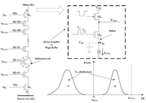
, level cell
bias read bias data
(read ) ,
cell Vth level
목 차 1. NAND Flash기술 및 동작소개 특성 소개 2. NAND Flash Erase
결 론 3.
동작 및 특성
NAND Flash Erase
서주완 (SK하이닉스반도체 최 민 충북대학교), ( )
,
data . ,
(program) (erase)
, target
Vth Vth
. cell Vth
Vth ,
.
, program under
program, cell x, y cell
(interference), ISPP step abnormal program cell, back pattern
Vth , Vth
level data
data . (-) Vth
erase cell program
disturbance cell Vth +
Vth . 0V
, read , read level 0V
fail .
cell interference disturbance
program erase (EW cycle)
.
high bias FN tunneling
tunnel oxide (trap site
) .
,
EW cycle cell
disturbance interference ,
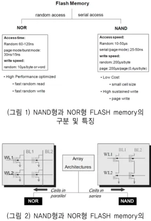
그림 형과 형 의
( 1) NAND NOR FLASH memory 구분 및 특징
그림 형과 형 의
( 2) NAND NOR FLASH memory 단위cell 구조
SLC : Erase cell (1) : Vth →-2V, Program Cell(0) : Vth → 2Vc
MLC : Erase cell(11) : Vth → -2V, program cell(’10’) : Vth→1V, Program cell(’00’) : Vth→ 2V, program cell(’01’) : Vth →3V
표 각 별
< 1> data state Cell Vth
Data(MLC) 11 10 00 01
Cell Vth -2V 1V 2V 3V
표 각 별
< 2> data state Cell Vth
EW cycle stress
NAND flash
. NAND
FLASH
, NAND cell
erase ,
.
NAND flash ,
.
그림 의 의 구분 방법
( 3) NAND FLASH logic '1', '0' (Cell Vth)
cell ‘0’
program
vth , ‘1’
erase vth
. , read , cell ‘1’
‘0’ .
program bulk floating
gate , erase
floating gate bulk , FN-tunneling
charge .
Program verify Erase verify , program , erase
cell vth , read ‘1’,
‘0’ , voltage
level target level
, level program verify level erase verify level ,
program erase bias ,
verify level cell inhibit (ex.
PGM cell bitline Vcc , FN
tunneling ) , Vth
.
Process ,
NAND flash cell , cell vth level
, Vth
‘1’, ‘0’
. data ,
그림 단위 에서의 및 시 조건 및 전하의 움직임
( 4) cell transistor program erase , bias .
(Program, Erase -
EW cycle) cell Vth
bias Vth
, program
cell vth level
(speed ), Vth
, erase cell Vth
level (speed ),
Vth . ,
EW cycle program program bias , erase
erase bias ,
Vth verify level
.
, program , erase
bias , ISPP ISPE
cell Vth level ,
( , ) Gate oxide
tunneling , erase
, bias ,
Vth shift Vth distribution
, bias ,
.
, ,
program erase ,
Cell Vth distribution bias
.
특성소개 2. NAND Flash Erase
NAND Flash erase erase
pulse , erase Vth level
,
erase verify . verify
(program verify ) ‘read’
. Program erase
, ‘read’ cell
‘1’ ‘0’ erase
program verify
Vth
. erase , erase pulse
, verify erase bias
.
erase verify , verify (-) level cell
, WL bias
cell erase . (
‘read’ read WL
bias(0V~5V ) bias ,
그림 알로리즘
( 5) ISPE flow chart
WL pass bias (~6V )
erase verify bias ,
(-) level cell Vth
) erase verify , cell string
WL bias , cell Vth variation
, cell string (current) , erase
verify .
(wordline) 0V~1V
bias , erase
, string
cell variation erase
speed , cell erase
verify , ISPE
bias erase
. 3 ISPE
.
erase verify ,
6 verify bias
verify bias
bias , 2
verify .
결 론 3.
NAND Flash
, SLC MLC,
TLC ,
SSD
. NAND Flash
,
. ,
NAND Flash 3D Stacking
. , NAND Flash
NAND
Flash / /
. ,
/ ,
.
그림 동작 개념
( 6) Erase Verify
참 고 문 헌
[ 1 ] Inside nand flash memories, Rino Micheloni, Springer
저 자 약 력
서 주 완
․․․․․․․․․․․․․․․․․․․․․․․․․․․․․․․․․․․․․․․․․․․․․․․
이메일 : [email protected]
∙2004년 광운대학교 전자재료공학과 학사( )
∙2016년 충북대학교 정보통신공학부 석사( )
∙2004 ~년 현재SK하이닉스반도체 책임연구원
∙ 관심분야:NAND Flash메모리 공정 임베디드 시스템,
최 민
․․․․․․․․․․․․․․․․․․․․․․․․․․․․․․․․․․․․․․․․․․․․․․․
이메일: [email protected]
∙2009년 한국과학기술원 전산학과 박사( )
∙2008 ~2010년 년 주 삼성전자 책임연구원( )
∙2011 ~년 현재 충북대학교 정보통신공학부 교수
∙ 관심분야 컴퓨터 시스템 임베디드 시스템,