Effective Transmission Method for low power RF systems
Jung-won Kim* , Ung-Se Choi*★
Abstract
In wireless communication system using 2.4GHz radio link, data rate varies with time due to interferences, which causes the performance degradation. Therefore, effective transmission methods are required to obtain better performance according to varying data rate. This paper proposes a novel method that increases the data rate, as well as the influence of different loop-filter bandwidths on the performance of the PLL. Experimental results show that the proposed method is effective because it can achieve higher throughput in various data rate.
Keywards: smartRF, WPAN, Tranceiver, PLL
* D ept. of Electr onics En gin eerin g, Korea Polytechnic Graduate School
★Corresponding author
Manuscript received Feb. 2, 2008 ; reviced May. 10, 2008
I. Introduction
Recently, a new universal radio interface, smartRF, has been developed enabling electronic devices to communicate wirelessly via short-range ad-hoc radio connections. The smartRF technology eliminates the needs of wires, cables and the corresponding connectors between cordless or mobile phones, head-sets, personal digital assistants (PDAs), computers, notebooks, printers, projectors, etc. WPAN provides wireless interconnections among the smartRF devices and peripherals used by individual. This network concept is called as wireless personal area network, WPAN [1, 2, 3, 4].
For applications of WPAN, the communication range of commercial smartRF is set to 10 m sufficient for the cable replacement [5,6]. Many advantages such
as wirelessness, mobility, and inter-operability expand the application areas of smartRF. In many applications, 10 m is not always a sufficient range.
To meet the requirement of longer communication range, the maximum range should be extended to 100m.
However, to extend communication ra nge, transmitter power should be increased. Increasing transmitter power causes more power consumption.
Because smartRF devices are almost portable, battery-driven equipment, low power consumption must be considered because of limited battery capacity. In general, for the devices that use battery power for other purposes such as cellular phones and PDAs, low power consumption is of critical interest. The transmit power level control is one of the solutions for low power implementation [7, 8].
By flexible power control in the smartRF transceiver, power consumption can be reduced when the transmitter range of smartRF is extended.
In spite of the importance of power control, it has not been studied yet.
In the current smartRF specification, the power control is optional but not defined yet [9,10].
In this paper, novel power control algorithms in smartRF transceiver are proposed. The control is focused on the uplink which means transmission link from a mobile station to a base station. The proposed power control algorithms are simulated under the indoor radio propagation model. By the simulation, the proposed algorithms can make the effective reduction of power consumption in smartRF devices.
This paper is organized as follows. In Section 2, the smartRF fundamentals of PLLs is introduced.
Section 3 shows some characteristics related to power control in smartRF. In Section 4, a Loop Filter Design is proposed with its mathematical description. Finally, conclusions are presented in Section 6.
II. Fundamentals of PLLs
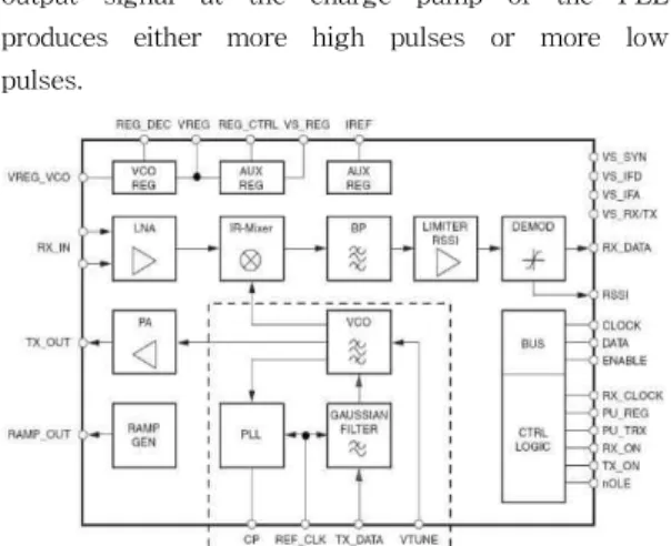
The phase-locked loop (PLL) compares the VCO frequency with the reference frequency which is derived out of the REF_CLK. Via the charge pump (CP) and the external loop (lowpass) filter, the output signal of the PLL is fed back into the VCO tuning input (VTUNE); the loop is closed.
In the case of a large difference between the VCO frequency and the reference frequency, the output signal at the charge pump of the PLL produces either more high pulses or more low pulses.
Fig. 1. Block Diagram of transceiver: VCO and PLL are in the Dashed Box.
These pulses are low-pass filtered by the loop filter. The corresponding DC voltage (VTUNE) will move the VCO frequency into the direction. The PLL will detect a match between VCO and reference frequency which corresponds to a charge pump out-signal that won't change VTUNE anymore.
To change the VCO or the output frequency, the reference frequency dividing factor of the PLL is programmed via the 3-wire bus interface.
The speed with which the tuning voltage settles to the right value is determined by two factors:
- The loop filter time constant, which defines the loop filter bandwidth
- The charge pump current
Also, the steepness of the VCO (Kvco) and the comparison frequency itself play a role in how fast the VCO is settled to the desired frequency.
The accuracy and stability of the RF output frequency is determined by the accuracy of the reference frequency.
Any frequency shift or noise of the reference frequency is directly viewable on the RF signal as well as the emitted RF spectrum.
The loop filter bandwidth plays a role in concerning the noise of the phase-locked VCO signal. This means that the higher the bandwidth, the more noise will be present on the phase-locked VCO, because the charge pump pulses are increasingly portrayed on VTUNE. There are several possibilities in frequency shift key (FSK) of a PLL synthesizer. They will be described in the next section.
III. Effective Transmission Method In this Section, some characteristics related to the power control are investigated. The power control s y s t e m o f s m a r t R F i s a l s o s t u d i e d .
III-I. Open-loop Modulation
To modulate the VCO, the loop is opened and TX_data is connected to the tuning voltage input of the VCO. Once the transmit burst is finished, the loop is closed again.
This way of modulating can often be found in applications. There are some issues to be kept in mind, however, because while modulating, the VCO is running free.
Any interference (feedback by power amplifier, etc.) coming into the opened loop (interfering with the oscillator and/or tuning voltage, for example, by a rectified RF signal) may cause an impact on the transmitted frequency and spectrum. This can result in frequency offsets or frequency drifts, The higher the capacitance of the loop filter, the lower the frequency drift; however, high capacitance lengthens the settling time of the PLL for locking on to the newly programmed frequency.
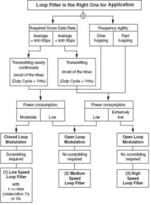
Fig. 3-1. Loop Filter Selection Chart
III-II. Closed-loop Modulation During closed loop modulation the PLL compensates for everything which de-tunes the VCO from its center frequency, because the PLL does not know which is interference and which is desired modulation. This big advantage for being immune to interference and feedback (as mentioned above in open-loop modulation) needs some consideration when modulating in a closed loop.
The ratio of bit-rate-to-loop-bandwidth has to be carefully chosen, or the applied modulation will be compensated by the PLL. Reducing the loop bandwidth to decrease the compensation speed of the PLL is one solution, however the settling time for the PLL will increase.
Another possibility is additionally modulating the phase detector comparison frequency oscillator, but this is not practical because the phase-detector comparison-frequency (which is derived from the reference clock) is also often used as a system clock within the base band controller, and so this would modulate the whole system clock.
A coding scheme which is DC-free is better-suited to keeping the average frequency value in the center of the RF channel.
Depending on the requirements and the phase detector reference frequency, a third-order loop filter might be needed to suppress the spurs caused by the reference frequency.
Ⅳ. Loop Filter Design
The following design procedure explains how to define a suitable loop filter for open-loop and closed-loop mode. If open-loop modulation is going to be used, the phase noise introduced by the loop-filter bandwidth plays a minor role since the phase noise will not be visible on the RF signal while transmitting.
Generally, for a fast settling time of the PLL, the loop-filter bandwidth has to be wide. However, in closed-loop mode, the PLL comparison frequency
has to be taken into calculation. This means that it may be necessary to add additional attenuation so that this frequency is supressed. A third pole at the loop filter can do this job. The advantage of a narrow loop filter in closed-loop mode is improved phase noise. Therefore, if closed-loop mode is going to be used on the target application, a compromise between settling time and phase noise has to be made.
The correct design of the loop filter is of considerable importance for the optimum performance of the synthesizer. The filter must be designed to achieve a good compromise between noise performance and settling time. The actual values of the parts used in the circuit will therefore depend on the particular application. A procedure has been established to ensure quick and simple loop-filter design. The method, based on first-order approximations, provides a working solution without the need for computer calculation.
Fig. 4-1. Third-order Loop Filter
Loop bandwidth fn using f n= 3 t s (1) Main divider ratio N using N = f r
f c (2) Angular velocity ω n (rad/s) using
ω n= 2 πfn (3)
The loop filter circuit has three time constants; they are
T 1= R 2C 1C 2
(C 1+C 2) (4)
T 2=R 2C 2 (5), T 3=R 3C 3 (6) The second order-loop is designed by omitting R3 and C3 (T3=0; R3=0; C3=0) and using the equations below:
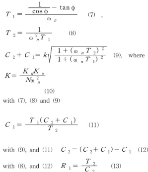
For a first step, use a phase margin of ϕ = 0.79 rad (ϕ = 45°).
T 1=
cos φ - tan1 φ
ω n (7) ,
T 2= 1
ω2nT 1 (8)
C 2+C 1=k 1 + ( ω nT 2) 2
1 + ( ω nT 1) 2 (9), where K = K dKo
Nω2n
(10) with (7), (8) and (9)
C 1= T 1(C 2+C 1)
T 2 (11)
with (9), and (11) C 2= (C 2+C 1) -C 1 (12) with (8), and (12) R 1= T 2
C 2 (13) Measuring the reference spurs and comparing them to a particular specification will determine if a third-order filter is necessary. During open loop (OL), the suppression of the reference frequency is not mandatory because the PLL-charge pump is disconnected from the VCO in this state.
V. Measurement Results
In this Section, the measurement results of power control in smartRF are presented. measurement scenario is as follows.
To do this, it is preferable to sleep most of the time, just wake up for a short moment, transmit the few bytes you need to transfer, and return to
sleep mode.
To transmit just a few bytes, it is not necessary to be able to transmit continuously, so short TX bursts are acceptable. Using open-loop modulation is a good choice for this application, and due to this, no scrambling is needed.
Therefore, the loop filter bandwidth [labelled (2) and (3) in Figure 3-1 on page 3] can be increased, enabling a faster settling time which results in a shorter wake-up time and makes fast changes of the frequency possible (that is, in less than 120 μs).
The Measurement parameters are as follows:
CH1: TX_ON CH2: nOLE CH3: 3W_ENB
CH4: BBA_OUT of reference RX (100 kHz/100 mV), center frequency is indicated by the horizontal cross line
PU_REG and PU_RXTX continuously on
Fig. 5. Measurement Results: 1n, 1k5, 10n, after TX_ON, PLL Settling 92μs
Ⅵ. Conclusion
In this paper, new power control methods for the smartRF transceiver are proposed : the fixed step power control and the dynamic step power control.
Experiments are performed with the indoor radio
propagation model results and shows the effectiveness of the proposed algorithms. Using the suggested power control, power consumption for the communication, which means transmission is reduced to about 40 percent of the commercial 100mW transceiver. In other words the mean time between two consecutive battery recharges will be extended to about 2.5 times.
However, the proposed power control is optional in the current smartRF specication so that additional hardware and software modules are required for the implementation.
References
[1] J. Haartsen and Mattisson S, "Bluetooth-a new low-power radio interface providing short-range conncectivity," Proceedings of the IEEE, vol. 88, pp. 1651{1661, 2000.
[2] M. Kalia S. Garg and R. Shorey, "Mac schedul- ing policies for power optimization in bluetooth: a master driven tdd wireless system," IEEE Vehic- ular Technology Conference, vol. 1, pp. 196{200, 2000.
[3] S. Mattisson, "Low-power considerations in the design of bluetooth," International Symposium on Low Power Electronics and Design, vol. 1, pp. 151{
154, 2000.
[4] T.S. Rapparport, "Wireless communication : Principle and practice," Prentice Hall, 1996.
[5] B. Sklar, "Rayleigh fading channels in mobile dig-ital communication systems," IEEE Communica- t i o n M a g a z i n e , v o l . 1 , p p . 1 3 6 { 1 4 6 , 1 9 9 7 . [6] J. Ziren, "Reliability of ieee 802.11 hi rate dsss wlans in a high density bluetooth environment,"
Bluetooth'99, pp. 1{12, 1999.
[7] http://grouper.ieee.org/groups/802/15/
[8] http://www.zigbee.org/
[9] TTA저널 제95호 [무선 사설망(WPAN) 기술] by 이형수|ETRI 위치인식 UWB team.
[10] Home networking with ZigBee” by Mikhail Galeev, www.nwfusion.com
http://junpasa.com/wireless/cdma/spreadspectrum.html
BIOGRAPHY Jung-won Kim (Member)
2002 : BS degree in Electrical Engineering, Korea Polytechnic University.
2004 : MS degree in Electrical Engineering, Korea Polytechnic University.
2008 : PhD courses at Electrical Engineering, Korea Polytechnic University.
2001~2004 : Research Engineer, Namsong Ind.
2004~ : Research Engineer, Changnam I.N.T
Ung-se Choi (Member)
1981 : BS degree in Electronics Engineering, Myong-Ji University.
1983 : MS degree in Electronics Engineering, Myong-Ji University.
1995 : PhD degree in Electronics Engineering, Myong-Ji University.
1981~1997 : Advanced Research Engineer, KITECH.
1997~ : Professor, Department of Electronics Enginnering, Korea Polytechnic University