DC 마그네트론 스퍼터링법으로 증착된 초박형 Al 박막의 투명전극 적용성 연구
김대균·최두호† 동의대학교 신소재공학부
Ultra-thin aluminum thin films deposited by DC magnetron sputtering for the applications in flexible transparent electrodes
Daekyun Kim and Dooho Choi†
School of Advanced Materials Engineering, Dong-Eui University, 176 Eomgwangro, Busan 47340, Korea (Received May 3, 2018: Corrected June 15, 2018: Accepted June 27, 2018)
초 록: 광전소자용 투명전극으로 적용하기 위한 초박형 Al 박막에 대한 기초연구를 수행하였다. 유리 기판 상에 3- 12 nm의 두께를 가지는 Al 박막을 형성하였으며, 박막의 두께가 7 nm 이상일 때부터 면저항이 측정되었으며 두께가 증 가할 때 면저항이 점진적으로 감소하였다. 박막 내 그레인 크기(Grain size)는 두께가 증가할수록 비례하여 증가하였다.
광 투과도의 경우 가시광선영역(380~770 nm) 파장 기준으로, 3 nm 박막 두께에서 평균 85%의 투과도가 측정된 데 반하 여, 4, 5 nm 두께에서 평균 50, 60%로 급격하게 감소되기 시작하며 그 이후 두께 증가에 따라 투과도가 점진적으로 감소 하였다. 본 연구결과는 향후 Oxide/Metal/Oxide(OMO) 구조의 고투과, 저저항 투명전극 적용을 위한 기초 결과로 활용될 것으로 기대된다.
Abstract: In this study, the feasibility of Al-based transparent electrodes for optoelectronic devices was investigated.
Al thin films having thickness in the range of 3-12 nm were deposited on glass substrates, and sheet resistance was measured for films thicker than 7 nm and the values continue to decrease with increasing film thickness. The grain size in the films was found to increase with increasing grain size. 85% visible light transmittance was measured at the thickness of 3 nm, and decreased to 50% and 60% when the film thickness reaches 4 nm and 5 nm, respectively. The results of this study can be used in the applications of oxide/metal/oxide type transparent electrodes.
Keywords: Sputtering, Aluminum, Thin film growth, Transparent electrode, Electrical resistance
1. 서 론
현재 디스플레이, 태양전지, 전기변색 소자 등 다양한 광전소자의 투명전극으로 높은 전기 전도도와 광학적 투 명성을 동시에 가지는 인듐 주석 산화물(Indium Tin Oxide, ITO)이 사용되고 있으나, 제한된 매장량으로 인한 고가의 인듐(Indium)이 사용되며 기계적인 자극에 의한 결함발생이 쉽고 휨성(Flexibility)이 부족하여 플랙서블 광전소자에 적용이 어렵다. 따라서 고투과, 저저항 특성 을 가짐과 동시에 유연성까지 보유한 유연투명전극의 개 발이 반드시 필요한 상황이며 현재 다양한 투명전도성 산 화물, Ag network1), graphene2), CNT3) 기반의 유연투명전 극 연구가 활발히 진행중이다. 뿐만 아니라 금속의 높은
전도성과 극박 두께에서의 높은 가시광선 투과도에 주목 하여 빛반사방지막인 산화물 샌드위치 층과 금속 박막을 결합한 Oxide/Metal/Oxide(OMO) 구조의 유연투명전극 연구가 진행중이다.4)
OMO 구조 형태의 투명전극에서의 투과도와 면저항은 트레이드 오프 (Trade-off) 관계를 가지는 데5), 이를 극복 하기 위해서는 극박 형태에서도 금속박막의 면저항의 증 가를 최소하는 것이 필요하다. 금속박막의 치수(두께, 선 폭, 그레인 사이즈 등)가 감소할 때 면저항이 증가하는 이 유는 전자의 표면 산란(Surface scattering)6,7) 및 결정립계 산란(Grain boundary scattering)8)으로 나타나는 현상인 비 저항 크기 효과(Resistivity size effect)가 더욱 심해지기 때 문이다. 이론적인 산란 모델6-8)에 따르면 이러한 비저항
†
Corresponding author E-mail: [email protected]
© 2018, The Korean Microelectronics and Packaging Society
This is an Open-Access article distributed under the terms of the Creative Commons Attribution Non-Commercial License(http://creativecommons.org/
licenses/by-nc/3.0) which permits unrestricted non-commercial use, distribution, and reproduction in any medium, provided the original work is
properly cited.
가 발생하는 초박형(<10 nm)구조에서 스퍼터링법으로 증 착된 Al박막의 비저항 크기 효과를 분석하였고 도출된 결과를 바탕으로 Al의 OMO 투명전극으로서의 활용가능 성에 대해 검토하였다.
2. 실험 방법
20 mm× 20 mm의 유리(Non-alkari glass, Corning E2000) 기판을 아세톤 용액과 IPA(Isopropyl Alcohol) 용액 내에서 각각 5분간 초음파 세척기를 이용하여 세척하였다. 증착 전 챔버의 기저압력(base pressure)은 3.0 × 10⁻⁷ Torr 이하였 으며, 99.999%의 Ar 가스 주입을 통해 압력을 1.0 × 10⁻² Torr로 상승시킨 후, 3 인치 크기의 Al (99.999 wt%) 스퍼 터 타겟을 이용하여 증착하였다. 증착 시, 타겟에 200W 의 DC 파워를 인가하였으며 기판의 회전속도는 15 RPM (Rotation Per Minute)로 유지하였다. 모든 증착과정에서 기판에 대한 인위적인 가열이나 냉각은 실시되지 않았다.
증착된 박막의 두께는 Alpha-step surface profiler(D-100, KLA Tencor)를 이용하여 측정하였으며, 도출된 증착률 3.1 Å/s을 바탕으로 박막의 두께를 결정하였다. 면저항 측정기(Four point probe)를 이용하여 박막의 면저항(Sheet Resistance)을 측정하였고, X-ray 회절(X-ray diffraction, XRD)을 이용하여 상분석을 실시하였으며, 주사전자현미 경(Scanning electron microscope, SEM)을 이용하여 표면
형상을 분석하였다. 박막 내 그레인 크기는 선교차법(line intercept method)10)을 이용하여 측정하였으며 시편당 평 균 120개의 그레인에 대한 평균값을 측정하였다. 적외-자 외-가시광선 분광계(UV-Visible spectrophotometer)를 이 용하여 200-1000 nm 파장대 영역에서의 광 투과도를 측 정하였으며, 광 투과도 측정 결과를 제시할 때 유리기판 자체의 투과도(약 8%)는 제외하였다.
3. 결과 및 고찰
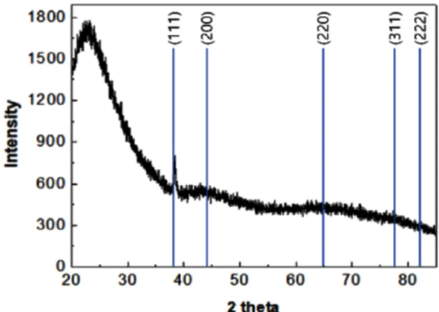
Fig. 1은 Al 박막의 θ −2θ X-선 회절 스캔 결과이며, 스 캔 범위는 20-100o이다. 약 25o부근에서의 넓은 피크는 유 리기판에서 기인하는 것이며11), Al 박막의 경우 (111) 회 절 피크만 관찰이 되었으며 이는 (111) 방향의 집합조직 을 가지는 것으로 결론을 내릴 수 있다.
Fig. 2는 3-12 nm 두께를 가지는 박막의 SEM 이미지이 다. Al 박막의 증착 거동은 아일랜드 구조의 핵이 초기에 생성되고 성장 단계를 거쳐 연속박막이 형성되는 Volmer- weber 유형12)을 따르는 것으로 확인되는 데, 두께가 증가 할수록 핵들의 합체(Coalescence)가 점진적으로 진행되지 Fig. 1. Theta-2theta XRD scan for the Al thin film deposited on
glass substrate.
Fig. 2. FE-SEM images showing the morphological changes as the films thicken from 3 to 12 nm.
만, 12 nm 두께까지도 완전한 연속박막을 형성하지 못한 것을 확인할 수 있다.
Fig. 3은 박막의 두께에 따른 면저항 측정 결과이며, 12 nm 두께에서 면저항이 6.5 Ω/Sq.로 가장 낮았으며 두 께가 줄어들수록 증가하였다. 5 nm 이하의 두께에서는 면 저항이 측정 장치의 최대값(2 MΩ/Sq.)을 초과하여 측정 이 되지 않았다. 면저항의 경우, 시간의 경과에 따라서 증 착 직후의 면저항 값과 비교하였을 때 각각 10-60% 상승 했으며 추가적인 증가는 관찰되지 않았다. 두께가 얇을 수록 변화폭이 상승하였는데, 이는 유리기판 상 증착된 Al 박막의 표면에 산화가 진행되어 알루미나(Alumina, Al2O3)가 형성이 되었고 두께가 얇을수록 잔류 Al 두께 또한 얇아지므로 면저항의 증가가 더욱 더 심해진 결과 라고 할 수 있다.
위와 같은 박막 두께의 감소에 따른 면저항의 증가는 서론에서 논의한 표면 및 결정립계 산란에 의한 전자 운 동량의 손실로 인한 결과이다. 이러한 비저항 크기 효과 는 흔히 볼츠만 운송 방정식(Boltzmann transport equation) 에 기초하여 유도된Fuchs-Sondheimer(FS) 표면 산란 모 델과 Mayadas-Shatzkes(MS) 결정립계 산란 모델을 이용 하여 전자운동량 손실에 대한 정량적 분석이 가능하다.
FS 모델은 표면 반사 파라미터(Surface specularity parameter)인 p를 포함하며, 이는 비저항 증가를 일으키지 않는 표면 거울반사 (specular scattering) 형태로 산란된 전자의 분율로 정의한다. 반면, 표면에서 난반사 (diffuse scattering)된 전자의 분율(1-p)은 초기 운동량을 상실하며 비저항의 증가에 기여한다. FS 모델에 의한 박막의 비저 항 식은 다음과 같다.
(1)
k = L/λ(L은 박막 두께, λ는 벌크 전자평균자유행로), ρ 는 벌크 비저항을 나타낸다. MS 모델은 주상(columnar) 결정립계에서 반사된 전자들의 분율로 정의되는 결정립 계 반사 계수(Grain boundary reflection coefficient) R을 포 함한다. (1-R)은 반사 없이 결정립계를 통과한 전자의 분
율을 나타낸다. 결정립계 산란과 표면 산란 사이에 상호 작용이 없고 박막의 두께가 무한한 경우, 결정립계 산란 에 의한 비저항 식은 다음과 같다.
α = (λ/g)(R/1-R), g는 면내(in-plane) 그레인 사이즈를 나 타낸다.13) 이러한 표면 산란 및 결정립계 산란 모델에서 비저항 크기 효과를 결정짓는 중요한 파라미터중의 하나 는 EMFP라고 할 수 있는데, 바꾸어 말하면 이 모델들은 비저항 크기 효과가 EMFP가 증가함에 따라 더욱 심각해 질 것으로 예상한다. 실제로 박막의 두께와 그레인 크기 가 EMFP와 유사하거나 그 이하로 감소될 경우, 벌크 영 역과는 달리 10 nm 이하 두께에서는 EMFP가 Cu보다 약 2.5배 더 짧은 Al 박막의 면저항이 Cu 박막의 면저항보 다 더 낮은 결과가 보고되었다.14)
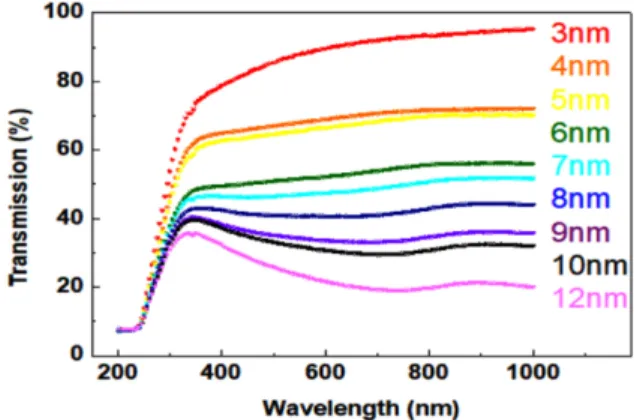
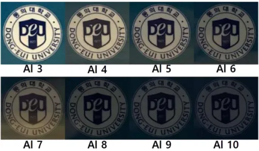
Fig. 4는 200-1000 nm의 파장 영역대에서의 3-12 nm의 두께를 가지는 Al 박막의 두께별 광 투과도를 나타내었 다. 가시광선 파장영역(380-770 nm) 내 평균투과도는 3 nm 두께에서 80% 이상의 투과도가 측정된 데 반하여, 4-5 nm 두께에서는 60% 대투과도로 급격하게 감소하였 고 6 nm 이상의 두께에서부터는 점진적으로 감소되는 결 과를 확인할 수 있었다. 이러한 광 투과도의 감소는 입사 광의 손실에 의해 일어나는데, 표면 반사효과와 더불어 증가에 따라 투과되는 입사광의 침투 깊이의 증가로 인 해 흡광도가 상승될 뿐만 아니라, 불연속 박막형태에서 의 아일랜드 구조에 의한 플라즈마 공명 효과 (plasmon resonance effect)에 기인한 결과이다.4) Fig 5는 광학적 투 과도를 실제로 보여주는 사진으로 박막의 두께가 증가할 수록 광 투과도가 감소하여 투명전극 하단에 위치한 피 사체가 흐릿하게 보이는 결과를 확인할 수 있었다. 본 논 문에서 연구한 Al 박막의 물성에 대해 Table 1에 정리하 였다.
위의 결과를 바탕으로 박막의 물성증진을 위해 Al전극 의 산화를 방지하고 빛반사를 저감하기 위하여 산화방지 ρFS pi 1 3
2k---
⎝ ⎠⎛ ⎞ 1 p( – ) 1 t3 --- 1
t5 –---
⎝ ⎠
⎛ ⎞ 1–exp(–kt) 1–exp(–kt) --- td
1
∫
∞– –1
=
ρMS pi 1 3–2---a 3a2 3a3 1 1 a---
⎝ + ⎠
⎛ ⎞ ln –
+ –1
= Fig. 3. Measured sheet resistance as a function of film thickness.
Fig. 4. Optical transmission of the Al films (3-12 nm) as a function of wavelength.
막 및 빛반사 방지막의 형성이 필요한 데, 기존 Cu와 Ag 을 기반으로 한 투명전극에 활용되었던 OMO (Oxide/
Metal/Oxide)구조4,5)의 도입을 통해서 이러한 목적을 효과 적으로 달성할 수 있을 것으로 기대된다. 하부 산화막의 경우에는 Al 박막의 젖음성 향상을 통해 Volmer-Webber 3D 성장모드를 억제시켜 연속박막 성장에 기여할 수 있 는 물질을 선정하여야 한다. 향후, 이러한 OMO 구조 및 물질의 최적화를 통해 면저항과 광 투과도 사이의 Trade off 현상을 최소화하여 투명전극으로써의 특성 극대화 연 구를 수행할 계획이다.
4. 결 론
Al 박막의 투명전극 적용연구를 수행하였다. DC 마그 네트론 스퍼터링법으로 유리 기판 상에 3-12 nm의 두께 를 가지는 Al 투명전극을 형성하였으며 투명전극의 주요
특성인 면저항과 광 투과도를 측정하였다. 면저항은 박 막두께가 6 nm 이상일 때부터 측정이 가능하였으며, 두 께가 증가할수록 지속적으로 감소하여 12 nm에서 가장 낮은 6.47 Ω/Sq.가 측정되었다. 광 투과도는 두께가 3- 5 nm에서 평균 60-80%의 가시광선 투과율이 측정되었으 나 그 이후 점진적으로 감소되는 경향을 확인할 수 있었 다. 주사전자현미경으로 촬영한 이미지를 확인한 결과 12 nm 두께의 박막에서도 완전히 연속된 박막의 형성이 이루어지지 않은 점이 상대적으로 높은 면저항과 낮은 광 투과도로 이어진 것으로 판단된다. 향후 Al 박막의 젖음 성 개선 연구와 산화방지 및 빛반사방지막 적용을 통해 향상된 투명전극 성능이 기대된다.
감사의 글
이 연구는 교육부 한국연구재단(이공) 과제(NRF- 2016R1D1A1B03931866) 지원으로 수행되었습니다.
References
1. J. H. Lee, P. Lee, H. M. Lee, D. J. Lee, S. S. Lee, and S. H.
Ko, “Very long Ag nanowire synthesis and its application in a highly transparent, conductive and flexible metal electrode touch panel”, Nanoscale, 4, 6408 (2012).
2. J. Wu, H. A. Becerril, Z. Bao, Z. Liu, Y. Chen, and P. Peu- mans, “Organic solar cells with solution-processed graphene transparent electrodes”, Appl. Phys. Lett., 92(26), 263302 (2008).
3. D. S. Hecht, D. Thomas, L. Hu, C. Ladous, T. Lam, Y. B.
Park, G. Irvin, and P. Drzaic, “Carbon-nanotube film on plas- tic as transparent electrode for resistive touch screens”, J. of the SID.,17(11), 941 (2009).
4. J. H. Yun, “Transparent Ultrathin Oxygen-Doped Silver Elec- trodes for Flexible Organic Solar Cells”, Adv. Funct. Mater., Fig. 5. Optical photographs of the Al electrodes having thickness of 3-10 nm.
Table 1. Film identification, thickness, sheet resistance, optical transmission and grain size for the films in this study. The listed optical transmission is average values over the visible light wavelengths (i.e., λ=380-770 nm).
Film id Thickness (nm)
Sheet resistance
(Ω/Sq.)
Ave-optical transmission (%)
Grain size (nm)
Al 3 3.1 - 88.0 22
Al 4 4 - 69.1 26
Al 5 5 - 61.9 33
Al 6 6.2 946.3 55.8 38
Al 7 6.8 135 49.2 41
Al 8 8.1 44.6 42.3 50
Al 9 9 20.1 37.5 45
Al 10 10.3 13.1 34.1 47
Al 12 12.1 6.5 23.7 46
24, 1551 (2014).
5. G. Zhao, W. Wang, T.-S. Bae, S.-G. Lee, C. W. Mun, S. H.
Lee, H. Yu, G.-H. Lee, M. K. Song, and J. H. Yun, “Stable ultrathin partially oxidized copper film electrode for highly efficient flexible solar cells”, Nat. com., 6, 8830 (2015).
6. K. Fuchs, “The conductivity of thin metallic films according to the electron theory of metals”, Proc. Cambridge Philos.
Soc., 34, 100 (1938).
7. E. H. Sondheimer, “The mean free path of electrons in met- als”, Advances in Physics,1(1), 1 (1952).
8. A. F. Mayadas, and M. Shatzkes, “Electrical-resistivity model for polycrystalline films: the case of arbitrary reflection at external surfaces”, Phys. Rev. B., 1, 1382 (1970).
9. D. Gall, “Electron mean free path in elemental metals”, J. of Appl. Phys., 119, 085101 (2016).
10. H. Abram, “Grain size measurement by the intercept method”, Metallography 4, 59 (1971).
11. Y. Shigesato, R. Koshi-ishi, T. Kawashima, and J. Ohsako,
“Early stages of ITO deposition on glass or polymer sub- strates”, Vacuum, 59, 614 (2000).
12. J. A. Floro, S. J. Hearne, J. A. Hunter, P. Kotula, E. Chason, S. C. Seel, and C. V. Thompson, “The dynamic competition
between stress generation and relaxation mechanisms during coalescence of Volmer–Weber thin films”, J. Appl. Phys., 89, 4886 (2001).
13. D. Choi, and K. Barmak, “On the potential of tungsten as next-generation semiconductor interconnects”, Electron.
Mater. Lett., 13, 449 (2017).
14. W. Zhang, S. H. Brongersma, O. Richard, B. Brijs, R. Pal- mans, L. Froyen, and K. Maex, “Influence of the electron mean free path on the resistivity of thin metal films”, Micro- electron. Engineer., 76, 146 (2004).
15. Y. Lantasov, R. Palmans, and K. Maex, “New plating bath for electroless copper deposition on sputtered barrier layers”, Microelectron. Engineer., 50, 441 (2000).
16. W. Zhang, S. H. Brongersma, T. Clarysse, V. Terzieva, E.
Rosseel, W. Vandervorst,and K. Maex, “Surface and grain boundary scattering studied in beveled polycrystalline thin copper films”, J. of Vac. Sci. & Technol. B., 22,1830 (2004).
17. C. Zhang, D. Zhao, D. Gu, H. S. Kim, T. Ling, Y. K. R. Wu, and L. J. Guo, “An ultrathin, smooth, and low loss Al doped Ag film and its application as a transparent electrode in organic photovoltaics”, Adv. Mater., 26, 5696?(2014).