• 검색 결과가 없습니다.

Electrical Loss Reduction in Crystalline Silicon Photovoltaic Module Assembly: A Review

N/A
N/A
Protected

Academic year: 2021

Share "Electrical Loss Reduction in Crystalline Silicon Photovoltaic Module Assembly: A Review"

Copied!
10
0
0

로드 중.... (전체 텍스트 보기)

전체 글

(1)

Nomenclature

V

OC

: open circuit voltage I

SC

: short circuit current FF: Fill Factor

P

max

: Maximum Power

Subscript

c-Si : crystalline silicon PV : photovoltaic CTM : cell-to-module

CTMV : cell-to-module variance CTE : coefficient of thermal expansion T&S : Tabbing and Stringing

R

ts

: Tabbing and Stringing Resistance

1. Introduction

PV modules are in huge demand among worldwide green energy resources as they are now used to supply electrical power and considered as good replacement of fossil fuel. The modules are fabricated by interconnecting number of solar cells in series through few steps. This processing leads to different loss and gain mechanisms.

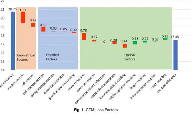
Due to this, the total output power of a module of series connected solar cells is less than the sum of the power of all solar cells. It is known as cell to module loss. Fig. 1 shows the factors that contributing in the final module efficiency reduction.

Several past research works have grouped those factors into three parts: Geometrical Factors, Optical Factors and Electrical Factors

1-4)

. The focus of this paper is to study the sources of electrical losses and how they can be optimized. From Fig. 1 we can observe that electrical loss accounts for 0.75% of overall reduction in cell to module efficiency. One of the key challenges to reduce electrical loss is to optimize untimely failure of solar cell interconnection. Interconnection is building the series connection between cells. It governs the electrical property of

Module Assembly: A Review

Sanchari Chowdhury

1)

․ Mallem Kumar

1)

․ Minkyu Ju

1)

․ Youngkuk Kim

1)

․ Chang-Soon Han

2)

․ Jinshu Park

1)

․ Jaimin Kim

1)

․ Young Hyun Cho

1)

* ․ Eun-Chel Cho

1)

* ․ Junsin Yi

1)

*

1)

College of Information and Communication Engineering, Sungkyunkwan University, Suwon, 16419, South Korea

2)

Technology Commercialization Team, Laser Advanced System Industrialization Center, Jangseong, 57258, South Korea Received July 18, 2019; Revised September 4, 2019; Accepted September 4, 2019

ABSTRACT: The output power of a crystalline silicon (c-Si) photovoltaic (PV) module is not directly the sum of the powers of its unit cells. There are several losses and gain mechanisms that reduce the total output power when solar cells are encapsulated into solar modules. Theses factors are getting high attention as the high cell efficiency achievement become more complex and expensive. More research works are involved to minimize the “cell-to-module” (CTM) loss. Our paper is aimed to focus on electrical losses due to interconnection and mismatch loss at PV modules. Research study shows that among all reasons of PV module failure 40.7% fails at interconnection. The mismatch loss in modern PV modules is very low (nearly 0.1%) but still lacks in the approach that determines all the contributing factors in mismatch loss. This review paper is related to study of interconnection loss technologies and key factors contributing to mismatch loss during module fabrication. Also, the improved interconnection technologies, understanding the approaches to mitigate the mismatch loss factors are precisely described here. This research study will give the approach of mitigating the loss and enable improvement in reliability of PV modules.

Key words: Photovoltaics, Solar cells, Solar modules, Interconnections, Mismatch, CTM

*Corresponding author: [email protected]; [email protected];

[email protected]

ⓒ 2019 by Korea Photovoltaic Society

This is an Open Access article distributed under the terms of the Creative Commons Attribution Non-Commercial License (http://creativecommons.org/licenses/by-nc/3.0)

which permits unrestricted non-commercial use, distribution, and reproduction in any medium, provided the original work is properly cited.

111

(2)

the module. Report says among all reasons of module failure

~40.7% PV modules fail due to interconnection

5)

. The inter- connections allow the electrical, thermal and mechanical contact between solar cell and electrodes. Temperature cycling during module’s field operation causes the degradation of soldering joints resulting in interconnection failure. Current challenge in PV module manufacturing is identifying the reli- ability of PV interconnections and approaching new soldering technologies. Another important factor to optimize electrical loss is reducing mismatch loss. Due to manufacturing variance and variation in operation condition, the individual cells opera- tion faces a deviation from their individual maximum power capacity. It causes a small loss in output power and is known as

“mismatch-loss”. Many research attempts are made to investi- gate the sources of mismatch loss which reduced its contribution in CTM loss to 0.05%. According to the reports of International Technology Roadmap for Photovoltaics, 0.0% mismatch loss is achievable in upcoming years

6)

. Also, junction box and cabling are key reasons of electrical loss which contributes 0.1% in overall CTM loss

7)

. This article reviews different sources of electrical loss factors and new approaches to improve them.

Also, new interconnection and soldering technologies, identifi- cation of reliable PV modules, examining the sources of mis- match loss discussed precisely. Aim of this review paper is to find appropriate technologies to enhance CTM ratio.

2. Types of Electrical Losses in PV module

2.1 Interconnection Loss and Calculation approach A single solar cell consists an array of gridlines of width <

0.4mm. Current in the solar cell is collected by busbars which is also metallization directly on the solar cell. Finer gridlines and low resistant busbars enable high I

SC

and FF

8)

. A set of c-Si solar cells are connected in series to from a string by cell interconnect ribbon during module fabrication

9)

. Multiple strings are associated with ‘string interconnect’. This is located nearly to the module edge and sometimes may be covered with module frame or cover layers

10)

. Fig. 2 shows a schematic diagram of cell interconnect and string interconnect. The challenges of interconnection process of c-Si cells in PV modules includes thermo-mechanical stress, series resistance and shadowing loss

11,12)

. Interconnection by soldering process is difficult and a high temperature process which occurs at about 250°C

13)

. The Infra-red reflow soldering involves high thermo-mechanical Fig. 1. CTM Loss Factors

Fig. 2. Cell Interconnection and String Interconnection

(3)

strain to the solder joints which may cause fatigue related damages. It is one of the key challenges of interconnection technology. Series resistance loss is another major challenge in interconnection technology. Metallization for contact formation and tabbing accounts for these losses. Calculating the con- version losses due to T&S is not simple and straight-forward.

Here we have discussed some approaches based on previous research. This suggests one diode model of a solar cell, as shown in Fig. 3, is a method which can be used to measure the conversion loss due to T&S

14)

. The relation between cell current (I) and voltage (V) satisfies the following equation

15)

:

I = I

ph

– I

0

[exp{(V+IR

S

)/nV

T

} – 1] = – (V+IR

S

)/R

Sh

(1)

Where, I

ph

: photo-generated current R

S

: series resistance R

Sh

: shunt resistance

I

0

: saturation current of the diode n: Ideality Factor

the effect of R

S

on maximum power (P

max

) of the cell can be quantified by using Eq. (1) and the CTM conversion loss due to T&S can be determined from the expression derived from above equation. Also, in Eq. (1) the total series resistance of a cell array consists of the bare cell resistance (R

so

) and resistance due to T&S (R

st

). Another approach is consid ered where a typical metallic ribbon makes contact all along the busbar lengths and behaves like a distributed resistance. In this configuration current is collected along the length of the busbars uniformly and flows through the fingers to the nearest busbars. After busbar collecting the current, full cell current is stored at the ribbon end. An accumulative equivalent of distributed resistance observed by the cell can be given by Eq. (2)

16)

.

R

ts

   

rib

W L

ribrib

t

rib

(2)

Where, ρ

rib

: resistivity of the metallic ribbon

L

rib

, W

rib

, t

rib

: length, width and thickness of the ribbon respectively

If there is a gap between the cells in an array, we can directly use the combined resistance. The cell-to-cell gap series re- sistance for a cell with two busbars can be given by following expression,

   

rib

W L

ribCTC

t

rib

and for a 3 busbars cell:

   

rib

W L

ribCTC

t

rib

Where, L

CTC

: length of cell-to-cell gap

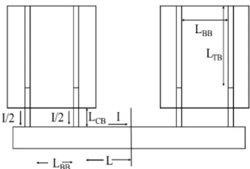
In the above expression the resistance due to busbars and the contact resistance is neglected. When the tabbed strings are connected in series by busing, an additional series resistance is introduced by busbars. Fig. 4 shows the schematic diagram of two strings connected in series and the current flow between them. For that configuration, the total resistance due to tabbing- stringing-bussing is given by Eq. (3)

17)

.

R

tsb

   

rib

 

W

rib

t

rib

L

TB

  

rib

 

W

rib

t

rib

L

CB

   

rib

 

W

rib

t

rib

L

BB

 

(3)

In the above equation, ρ

rib

, W

rib

, t

rib

is the resistivity, width and thickness of the ribbon respectively. W

Brib

, t

Brib

are the width and thickness of bussing ribbon respectively. L

TB

is the length of the soldered ribbon. L

CB

is the distance between cell edge and bussing ribbon and L

BB

is the length between two extreme busbars of a single cell. When the bare cell parameters – V

OC

, Fig. 3. One Diode Model of Solar Cell

Fig. 4. Cell Interconnection and Current Flow between them

(4)

mation of series resistance due to tabbing-stringing-bussing is possible by using Eqs. (2) and (3). In addition, the bare cell resistance is a dominating factor in lower efficiency cells which makes the conversion loss at T&S lower. On the other hand, the loss is higher for high efficiency cells.

Another substantial challenge of interconnection technology is shadowing losses. A wider cell requires a thicker inter- connection ribbon for conducting larger currents. Reports

18)

suggests that shadowing losses increases proportionally with the increase in the width of the interconnection ribbon. the ribbon strip thickness is restricted by the stress accumulated at the solder joint. The differences in the coefficient of thermal expansion between silicon wafer and interconnection ribbon material is the reason of this stress

19)

. Additionally, the bending of the interconnection ribbons at the edge of the wafer causes further stress. This affects the reliability of the whole module assembly

20-24)

. In the later section we will discuss about the approaches to reduce the interconnection losses.

2.2 Electrical Mismatch Losses and the calculation approach

Mismatch loss is the difference between the maximum power of a PV module and the total sum of maximum powers of individual cells connected in module. When the cells are encapsulated into module a broader group of changes occur which results in mismatch loss. Optimization in module manufacturing strategies requires proper understanding of mismatch loss. This section reviews the mismatch loss related to electrical interconnection. The loss mechanism which impact the mismatch loss will give an idea to module manufacturers.

2.2.1 Theoretical mismatch loss for interconnection When the cells are interconnected in series to develop a module, the mismatch loss is proportional to the variance of maximum power current (I

mp

)

25,26)

, given by following equation:

Series Loss∞

Imp

(4)

σ

Imp

is the standard deviation of the maximum power current.

The typical value of this standard deviation is in the range of 0.5% - 0.6% which accounts for 0.02% - 0.04% loss. But the Eq (4) will be valid only when the interconnected devices will

applicable . Similarly, when the cells are connected parallelly, the mismatch loss becomes proportional to the variance of the maximum power point voltage (V

mp

). The equation is a s follows

Parallel Loss∞

Vmp

(5)

σ

Vmp

is the standard deviation of the maximum power point voltage

33)

. Eq. (5) is free from reverse bias fault risk and appli- cable for a wider range of standard deviation values of V

mp

.

2.2.2 Mismatch Loss due to cell-to-cell variance The variance in the cell’s performance leads to mismatch loss and is known as “module level” mismatch loss. Previously this loss had a huge impact on module development

33,34)

but in modern photovoltaic technologies the effect is so small and is virtually unmeasurable

35,36)

because modern cell performances show less variance when fabricated in mass production. After the fabrication of the photovoltaic cells they are uniformly sorted based on their current or power. The main purpose of the cell sorting is to reduce the cell-to-cell variance. When enough cells are sorted to make a module

37)

they are combined to form a “cell packet”. Average electrical performance of the cell consisted the cell packet determines the electrical performance of the module developed from those cells. Though it can not be determined perfectly because some variances are introduced during module fabrication process. This is known as Cell to Module Variance (CTMV).

2.2.3 Mismatch loss due to module-to-module variance Variance in module performance attributes to mismatch loss when they are interconnected in an array. This is known as

“array level” mismatch loss. If they are interconnected in a typical series strings Eq. (4) will be applied and for parallel interconnection Eq. (5) can express the loss. To optimize this loss the modules are also sorted according to their I

mp

and V

mp

. Research study says that the module sorting to reduce mismatch loss is not a zero-cost process and it may affect the overall cost in large scale production

38-41)

.

2.2.4 Loss due to cell-to-module variance

Previously we have discussed the interconnection and

(5)

difference between the final module variance and the variance of cell packet average. The relation is shown in Eq. (6)

43)

CTM

 

Mod

 

cpAv

(6)

for a perfect module i.e. 0 CTM loss it should be σ

2Mod

= σ

2cpAv

. The σ

CTM

is important to calculate the variances of I

mp

and V

mp

. If Vmp is changed the additional series resistance is changed as well as σ

CTM

. Changes in Imp is related to the optical effects during encapsulation process.

2.3 Mismatch Loss Calculation Approach

From past research works three attempts have been identified to compute the mismatch loss at the final stage of module development

44-46)

. One of them is significantly important as the only approach that measures the mismatch loss at the ultimate module level via direct experimentation. Though this technique is not enough to accurately calculate the loss for modern manufacturing techniques, and it is not a general method for all module manufacturing strategies. The second method is a mathematical model built for CTM effects which includes mismatch. The third approach is using the expected difference values between module I-V curve and suns-V

OC

curve to obtain the mismatch loss. Though these two approaches are designed in such a manner that they cannot deal with non-standard condition.

So, they cannot detect relatively small mismatch accurately.

Later in recent years another approach has been made to overcome the drawbacks of the above methods. Here a hypo- thetical module of 72 component cells has been considered

47)

. The I-V curves of production cells are summarized to form the I-V curve of the hypothetical model and calculate the maximum power and maximum current from the curve. The hypothetical curve is assumed to have no additional series resistance due to interconnections or changes in cell current due top encap- sulation

48)

. The mismatch loss is obtained by calculating the difference between the sum of maximum powers of 72 different cells and the maximum power of the hypothetical model. The calculation of mismatch loss is as following equation:

L   ∑

i  

p

i

i  

p

i

 P

max

(7)

Where, p

i

= maximum power of i

th

cell

P

max

= maximum power of the hypothetical module This approach is the most direct approach of mismatch loss estimation which is validate for modern technologies based on power-current relationship.

2.4 Junction Box Failure

Junction Box protects the cell strings connection to the external terminal. Generally, the box contains the bypass diodes that protects the cell from hot spot or shadowing

49)

. But the improper design or incorrectly disclosed junction boxes causes corrosion to the junction box connections due to the moisture entered. This causes wiring failure that results in internal arcing and arcing can initiate fire

50)

. Also, back-sheet delamination near junction box causes an unconstrained stress which further introduces a mechanical stress on the components and break them

51)

.

3. Challenges in optimizing Electrical Loss in PV module

3.1 Interconnection Technology reliability challenge Previous reports claim that degradation in interconnection occurs as the PV modules are subjected to regular thermal cycles during their in-field operation

52)

and introduces additional series resistance

53)

. Interconnections in solar cells are primarily done by two techniques. One is soldering technology, and another is using electrically conductive adhesive

54)

. In the following sections we will discuss about the reliability of these two technologies on the system performance and degradation during operation. Fig. 5 shows the current market share and future progress of different cell interconnection technologies.

Fig. 5. Recent and expected market share of different cell inter-

connection technologies

(6)

between ribbon and electrode. The current flows from silicon wafer to ribbon through this connection. The materials like solder, bus-bar, ribbon and silicon wafer are bonded together at the joint. The differences in the coefficient of thermal expansion of those materials are the reasons of thermo-mechanical reliability problems. Soldering technology is a high temperature process. During the process the shearing force on silicon wafer is introduced due to the differences in coefficient of thermal expansions of the bonding materials. This results in fatigue damage in the module as well as grid finger interruption at the edges of bus-bar

55)

. Furthermore, the local weather is a key factor that affects the PV module temperature. This influences the degradation of solder interconnection. Lifetime prediction analysis reports claim that same type of c-Si PV modules installed in various locations show different lifetimes

56)

. The daily temperature cycle and moisture is involved in metal degradation, cracked grain boundary, additional series resistance and heating

57)

. To avoid the conventional soldering problems, researchers developed laser soldering technology for various PV module designs. This technology is highly reliable as it introduces reduced mechanical and thermal stress in solder joints. An experimental investigation report

58,59)

suggests that a conventional soldering method induces a peel force ranged between 1-3 N while for laser soldering technology the force is nearly equal to zero. Hence this technology causes less damage in solar cell interconnection. It can be concluded that in near future laser soldering technology can produce reliable and cost-effective interconnection technology.

3.1.2 Electrically Conductive Adhesive Technology The high temperature soldering technology actuate stress and the on-field operation brings deformation in solar cell. These results in cell distortion, rupturing, cracking and overall module failure. To avoid the above problems the use of electrically conductive adhesive for cell interconnection technology has been adapted. The adhesive, made of silver loaded epoxy resins, are used as alternative bonding to interconnect solar cells

60-62)

. since the process is the low temperature it implants low residual stress on joint resulting in less module failure. Also, mechanical properties of the bonded materials at joint subjects to optimal changes due to the use of conductive adhesive and the electrical conductivity at the joint increases. Still this process is associated

results in crack, corrosion and system failure.

3.2 Challenges in Mismatch Loss Estimation in field The mismatch loss for a given set of module categories in the field is influenced by manufacturing and design related factors.

For a particular field installation, the modules are sorted according to their power rating with tolerance and current. In addition to that solar irradiation and temperature uniformity also affects the mismatch factors. Previously research works were done on the mismatch loss due to separate type of modules in a large fielded array, the mismatch loss related to the difference between theoretical and actual measured power of module, considering mismatch loss as a function of installation condition and their tolerance power. But there are still some factors which is yet to be considered. One of them is the variation in the condition experienced by individual module operating in the field an array. Also, the precision of the power measuring instrument in a field condition is ignored. The attempt of on-spot calculation of actual mismatch loss of an operating system was not considered yet

63,64)

. Power optimizers used to eliminate mismatch loss arguably have no other design features in the array system to reduce mismatch loss. So, when the result is generalized in standard field the loss may be over extended. If the solar panels are chosen according to their power rating and no other sorting, this also do not have an accurate measurement of mismatch loss – it can either be improved or declined

65)

. The daily sky conditions also have key influence on the mismatch loss. If the average calculation of mismatch loss is done on clear sky day and cloudy day the value will not be same for the two.

Due to no shading loss issues on clear sky day. Another

important factor is inverter that converts solar energy into

electrical energy

66)

. A single central inverter is used to invert

energy at every string and simultaneously eliminate parallel

mismatch loss, but if the modules are not sorted accordingly the

inverters used at group of string make an optimal deference. The

three most important factors that needs to be focused to reduce

mismatch loss are invariable illumination, uniform temperature

and relation between performance under simulated light

condition and performance on field condition

67)

. Also, the

manufacturing and field designs are similarly important in low

mismatch loss.

(7)

minimize electrical losses and several challenges are discussed earlier but no single technique was succeeded to overcome all the challenges. Therefore, more research works needed for cell design and manufacturing. Research work to optimize CTM electrical loss is focused on optimizing series resistance, shadowing and recombination loss, mismatch loss module degradation and induced thermo-mechanical stress. Series resistance mainly arises due to through emitter and base solar cell, contact between metal and silicon and the resistance due to top and rear metal contact. Further research is needed to reduce metal contact resistivity which can also improve the energy conversion efficiency. Interconnection ribbon on the c-Si wafer surface induces shadowing loss. This increases with the increase in interconnection width. To avoid this problem the technology of interconnection at the back of cell is introduced however the technology is complex and expensive. Thus, further development in reducing shadowing loss is required.

Thermo-mechanical stress due to the difference between CTE of bonding materials at interconnection causes module de- gradation and system failure. The parameters of module manufacturing design such as busbar, ribbon, back-sheet dimensions needed to be set accordingly to improve the PV module reliability. Additionally, more improvement is required for conductive electric adhesive required for interconnection to make the PV module more durable and reliable. Mismatch loss reduction approach loss in PV module has developed many theoretical equations and cell sorting methods but that do not involve all the key factors responsible for them mainly the single field conditions. Also, cell sorting increases module variance and further cost is associated with this. The cell sorting for high volume manufacturing does not have a fixed cost and some- times may be too expensive which further increases the module price. Further cost increases with the system developed for designing and installing modules of different power ratings.

Still the manufacturing technology requires cell sorting based on cell color for maintaining product standard and thermal breakdown characteristics for ensuring safety. This concludes further research opportunity for developing more improved cell sorting algorithms that will reduce mismatch loss as well as develop cost effective module systems.

nisms due to interconnection, mismatch and junction box failure during cell-to-module fabrication. The new technological and theoretical approaches to optimize the loss was also discussed.

The proper electrical interconnection technology and novel module design can reduce CTM loss up to 0.0%. It was shown that basic pre-dominant interconnection technology induces thermo-mechanical stress in the cell and joints, increases series resistance and shadowing losses. This paper identified that laser soldering technology and conductive adhesive soldering can overcome those problems and can produce a highly reliable module. Though the adhesive-metal bonding initiates some substantial crack resulting into corrosion induced system failure. It seems major research work in tooling and manu- facturing facilities still requires optimizing CTM loss further.

Also, we assessed that installation-related issues have significant role in mismatch loss. Better understanding and accurate in-situ loss estimation can minimize the mismatch loss further and cost optimization needs the attention. This paper reviewed all the potential factors occurring mismatch loss and identified some calculation approaches. Further research scopes in cost re- duction and loss mitigation strategy was also described.

Acknowledgments

This work was supported by the Korea Institute of Energy Technology Evaluation and Planning(KETEP) grant funded by the Korea government(MOTIE) (Project No. 20193010014850) and This work was conducted under the framework of the New and Renewable Energy Technology Development Program of the Korea Institute of Energy Technology Evaluation and Planning (KETEP) through a grant funded by the Ministry of Knowledge Economy, Korea (Project No. 20163020010890).

References

1. Hanifi, H., Pfau, C., Dassler, D., Schneider, J., Schindler, S., Turek, M. and Bagdahn, J., “Investigation of cell-to-module (CTM) ratios of PV modules by analysis of loss and gain mecha- nisms,” Photovoltaics Int, Vol. 32, pp. 89-99, 2016.

2. Witteck, R., Hinken, D., Müller, J., Blankemeyer, S., Bothe,

K., Schulte-Huxel, H., Köntges, M. and Brendel, R., “Simulation

of optimized cell interconnection for perc modules exceeding

(8)

diction of module power,” Sol. Energy Mater. Sol. Cells, Vol.

131, pp. 14-23, 2014.

4. Hanifi, H., Dassler, D., Schneider, J., Turek, M., Schindler, S.

and Bagdahn, J., “Optimized tab width in half-cell modules,”

Energy Procedia, Vol. 92, pp. 52-59, 2016.

5. Zarmai, M.T., Ekere, N.N., Oduoza, C.F. and Amalu, E.H.,

“A review of interconnection technologies for improved crys- talline silicon solar cell photovoltaic module assembly,” Appl.

Energy, Vol. 154, pp. 173-182, 2015.

6. SEMI, P., 2016. Group 2012, International Technology Road- map for Photovoltaic (ITRPV. net), Results 2011.

7. Mittag, M., Kutter, C., Hoffmann, S., Romer, P., Beinert, A.J.

and Zech, T., “Electrical and thermal modeling of junction box- es,” 33rd EUPVSEC, Amsterdam, pp. 1501-1506, 2017.

8. Geipel, T., Moeller, M., Walter, J., Kraft, A. and Eitner, U.,

“Intermetallic compounds in solar cell interconnections:

Microstructure and growth kinetics,” Sol. Energy Mater. Sol.

Cells, Vol. 159, pp. 370-388, 2017.

9. Zarmai, M.T., Ekere, N.N., Oduoza, C.F. and Amalu, E.H.,

“A review of interconnection technologies for improved crys- talline silicon solar cell photovoltaic module assembl,” Appl.

Energy, Vol. 154, pp. 173-182, 2015.

10. Tsunomura, Y., Yoshimine, Y., Taguchi, M., Baba, T., Kinoshita, T., Kanno, H., Sakata, H., Maruyama, E. and Tanaka, M., “Twenty-two percent efficiency HIT solar cell,”

Sol. Energy Mater. Sol. Cells, Vol. 93(6-7), pp. 670-673, 2009.

11. Zarmai, M.T., Ekere, N.N., Oduoza, C.F. and Amalu, E.H.,

“A review of interconnection technologies for improved crys- talline silicon solar cell photovoltaic module assembly,” Appl.

Energy, Vol. 154, pp. 173-182, 2015.

12. Kerschaver, E.V. and Beaucarne, G., “Back ‐contact solar cells:

A review,” Progress in Photovoltaics: Research and Applications, Vol. 14, No. 2, pp. 107-123, 2006.

13. Anguiano, C., Félix, M., Medel, A., Bravo, M., Salazar, D. and Márquez, H., “Study of heating capacity of focused IR light sol- dering systems,” Opt. Express, Vol. 21, No. 20, pp. 23851- 23865, 2013.

14. Schneider, A., Harney, R., Aulehla, S., Lemp, E. and Koch, S.,

“Progress in interconnection of busbar-less solar cells by means of conductive gluing,” Energy Procedia, Vol. 38, pp. 387-394, 2013.

15. Park, S., Cho, E., Song, D., Conibeer, G. and Green, M.A.,

“n-Type silicon quantum dots and p-type crystalline silicon het- eroface solar cells,” Sol. Energy Mater. Sol. Cells, Vol. 93, No.

6-7, pp. 684-690, 2009.

16. Jung, T.H., Song, H.E., Ahn, H.K. and Kang, G.H., “A mathe- matical model for cell-to-module conversion considering mis- matching solar cells and the resistance of the interconnection ribbon,” Solar Energy, Vol. 103, pp. 253-262, 2014.

module (CTM) conversion loss during c-Si Solar Photovoltaic (SPV) module manufacturing,” Solar Energy, Vol. 130, pp.

184-192, 2016.

19. Kerschaver, E.V. and Beaucarne, G., “Back ‐contact solar cells:

A review,” Progress in Photovoltaics: Research and Applications, Vol. 14, No. 2, pp. 107-123, 2006.

20. Bultman, J.H., Weeber, A.W., Brieko, M.W., Hoornstra, J., Burgers, A.R., Dijkstra, J.A., Tip, A.C. and Schuurmans, F.M., “Pin up module: a design for higher efficiency, easy mod- ule manufacturing and attractive appearance,” In Proceedings of the 16th EPVSC, Glasgow, pp. 1210-1213, 2000.

21. Wendt, J., Träger, M., Mette, M., Pfennig, A. and Jäckel, B.,

“The link between mechanical stress induced by soldering and micro damages in silicon solar cells,” Proc. of 24th EUPVSEC, Hamburg, Germany, 2009.

22. Gabor, A.M., Ralli, M., Montminy, S., Alegria, L., Bordonaro, C., Woods, J., Felton, L., Davis, M., Atchley, B. and Williams, T., “Soldering induced damage to thin Si solar cells and de- tection of cracked cells in modules. In 21st European Photovol- taic Solar Energy Conference, pp. 4-8, 2006.

23. Söderström, T., Papet, P. and Ufheil, J., “September. Smart wire connection technology,” In the 28th European Photovol- taic Solar Energy Conference, pp. 495-499, 2013.

24. Munoz, M.A., Alonso-García, M.C., Vela, N. and Chenlo, F.,

“Early degradation of silicon PV modules and guaranty con- ditions,” Solar energy, Vol. 85, No. 9, pp. 2264-2274, 2011.

25. Suzuki, S., Doi, T., Masuda, A. and Tanahashi, T., “Bending cyclic load test for crystalline silicon photovoltaic modules,”

Jpn. J. Appl. Phys., Vol. 57, No. 2S2, pp. 02CE05, 2018.

26. Bucciarelli Jr, L.L., “Power loss in photovoltaic arrays due to mismatch in cell characteristics,” Solar Energy, Vol. 23, No. 4, pp. 277-288, 1979.

27. Evans, R. and Boreland, M., “Multivariate analysis of wafer process data,” In Proc. 30th Eur. Photovolt. Sol. Energy Conf, 2008.

28. Kaushika, N.D. Rai, A.K., “An investigation of mismatch loss- es in solar photovoltaic cell networks,” Energy, Vol. 32, No. 5, pp. 755-759, 2007.

29. Alonso-Garcia, M.C., Ruiz, J.M. Chenlo, F., “Experimental study of mismatch and shading effects in the I-V characteristic of a photovoltaic module,” Sol. Energy Mater. Sol. Cells, Vol.

90, No. 3, pp. 329-340, 2006.

30. Roche, D., Outhred, H., Kaye, R.J., “Analysis and control of mismatch power loss in photovoltaic arrays,” Progress in Photovoltaic, Vol. 3, No. 2, pp. 115-127, 1995.

31. Park, C., Yoon, N., Min, Y.K., Ko, J.W., Lim, J.R., Jang, D.S., Ahn, J.H., Ahn, H., “Numerical Analysis of Si-based Photovoltaic Modules with Different Interconnection Methods,”

Transactions on Electrical and Electronic Materials, Vol. 15,

(9)

217-233, 2003.

33. Jung, T.H., Ko, J.W., Kang, G.H., Ahn, H.K., “Output char- acteristics of PV module considering partially reverse biased conditions,” Solar Energy, Vol. 92, pp. 214-220, 2013.

34. Mäki, A., Valkealahti, S., “Power losses in long string and par- allel-connected short strings of series-connected silicon-based photovoltaic modules due to partial shading conditions,” IEEE Transactions on Energy Conversion, Vol. 27, No. 1, pp.

173-183, 2012.

35. Kaushika, N.D. Rai, A.K., “An investigation of mismatch loss- es in solar photovoltaic cell networks,” Energy, Vol. 32, No. 5, pp. 755-759, 2007.

36. Bucciarelli Jr, L.L., “Power loss in photovoltaic arrays due to mismatch in cell characteristics,” Solar Energy, Vol. 23, No. 4, pp. 277-288, 2012.

37. Bishop, J.W., “Computer simulation of the effects of electrical mismatches in photovoltaic cell interconnection circuits,”

Solar cells, Vol. 25, No. 1, pp. 73-89, 1988.

38. Webber, J., Riley, E., “Mismatch loss reduction in photovoltaic arrays as a result of sorting photovoltaic modules by max-pow- er parameters,” ISRN Renewable Energy, 2013.

39. Wilson, K., De Ceuster, D., Sinton, R.A., “Measuring the ef- fect of cell mismatch on module output,” IEEE 4th World Conference on Photovoltaic Energy Conference, Vol. 1, pp.

916-919, 2006.

40. Chamberlin, C.E., Lehman, P., Zoellick, J., Pauletto, G.,

“Effects of mismatch losses in photovoltaic arrays,” Solar en- ergy, Vol. 54, No. 3, pp. 165-171, 1995.

41. Kaushika, N.D. and Rai, A.K., “An investigation of mismatch losses in solar photovoltaic cell networks,” Energy, Vol. 32, No. 5, pp. 755-759, 2007.

42. MacAlpine, S., Deline, C., Erickson, R. and Brandemuehl, M.,

“Module mismatch loss and recoverable power in unshaded PV installations,” IEEE Photovoltaic Specialists Conference, pp.

001388-001392, 2012.

43. Iannone, F., Noviello, G., Sarno, A., “Monte Carlo techniques to analyse the electrical mismatch losses in large-scale photo- voltaic generators,” Solar energy, Vol. 62, No. 2, pp. 85-92, 1998.

44. Lappalainen, K., Valkealahti, S., “Output power variation of different PV array configurations during irradiance transitions caused by moving clouds,” Appl. Energy, Vol. 190, pp. 902-910, 2017.

45. Evans, R., Kim, K.H., Wang, X., Sugianto, A., Chen, X., Chen, R., Green, M.A., “Simplified technique for calculating mismatch loss in mass production,” Sol. Energy Mater. Sol.

Cells, Vol. 134, pp. 236-243, 2015.

46. Gasparin, F.P., Bühler, A.J., Rampinelli, G.A., Krenzinger, A., Statistical analysis of I-V curve parameters from photovoltaic

2010.

48. Evans, R., Kim, K.H., Wang, X., Sugianto, A., Chen, X., Chen, R., Green, M.A., “Simplified technique for calculating mismatch loss in mass production,” ol. Energy Mater. Sol.

Cells, Vol. 134, pp. 236-243, 2015.

49. Saha, H., Bhattacharya, G., Mukherjee, D., “Mismatch losses in series combinations of silicon solar cell modules,” Solar cells, Vol. 25, No. 2, pp. 143-153, 1998.

50. Chung, I., young Son, H., Oh, H., Baek, U.I., Yoon, N., Lee, W.J., Cho, E.C., Moon, I.S., “Light Capturing Film on inter- connect ribbon for current gain of crystalline silicon PV mod- ules,” IEEE 39th Photovoltaic Specialists Conference, pp.

1478-1480, 2013.

51. Jung, T.H., Song, H.E., Ahn, H.K., Kang, G.H., “A mathe- matical model for cell-to-module conversion considering mis- matching solar cells and the resistance of the interconnection ribbon,” Solar Energy, Vol. 103, pp. 253-262, 2014.

52. Gupta, M., Dubey, A.K., Kumar, V., Mehta, D.S., “Solar con- centrator based multipurpose sunlight harvesting system with- out tracking,” OSA Continuum, Vol. 2, No. 3, pp. 667-676, 2019.

53. Wohlgemuth, J., Cunningham, D.W., Nguyen, A., Kelly, G., Amin, D., “Failure modes of crystalline Si modules,” In PV Module Reliability Workshop, 2010.

54. Dhere, N.G., “Reliability of PV modules and balance-of-sys- tem components,” In Conference Record of the Thirty-first IEEE Photovoltaic Specialists Conference, pp. 1570-1576, 2005.

55. Cristaldi, L., Faifer, M., Lazzaroni, M., Khalil, A.F.M.M., Catelani, M., Ciani, L., “Failure modes analysis and diagnostic architecture for photovoltaic plants,” In Proccedings of the 13 th IMEKO TC10 Workshop on Technical Diagnostics Advanced measurement tools in technical diagnostics for systems’ reli- ability and safety, pp. 206-211, 2014.

56. Wohlgemuth, J.H., “Reliability of PV systems. In Reliability of Photovoltaic Cells, Modules, Components, and Systems,”

International Society for Optics and Photonics, Vol. 7048, pp.

704802, 2008.

57. Zemen, Y., Prewitz, T., Geipel, T., Pingel, S., Berghold, J.,

“The impact of yield strength of the interconnector on the in- ternal stress of the solar cell within a module,” In 25th European Photovoltaic Solar Energy Conference and Exhibi- tion, pp. 4073-4078, 2008.

58. Kurtz, S., Granata, J., Quintana, M., “In Reliability of Photovoltaic Cells, Modules, Components, and Systems II,”

International Society for Optics and Photonics, Vol. 7412, p.

74120Z, 2009.

59. Grunow, P., “Soldering of crystalline silicon modules: Losses,

reliability and improvements,” In 2nd Workshop on Metalliza-

tion of Crystalline Silicon Solar Cells, 2010 .

(10)

61. Wendt, J., Träger, M., Mette, M., Pfennig, A., Jäckel, B., “The link between mechanical stress induced by soldering and micro damages in silicon solar cells,” Proc. of 24th EUPVSEC, Hamburg, Germany, 2009.

62. Dhere, N.G., “Reliability of PV modules and balance-of-sys- tem components”. In Conference Record of the Thirty-first IEEE Photovoltaic Specialists Conference, 2005. pp. 1570-1576.

IEEE. 2005.

63. Schmidhuber, H., Klappert, S., Stollhof, J., Erfurt, G., Eberspächer, M., Preu, R., “Laser soldering-a technology for better contacts,” In 20th European Photovoltaic Solar Energy Conference, pp. 1-4, 2005.

64. Tsanakas, J.A., Ha, L., Buerhop, C., “Faults and infrared ther- mographic diagnosis in operating c-Si photovoltaic modules: A review of research and future challenges,” Renewable and sus- tainable energy reviews, Vol. 62, pp. 695-709, 2016.

65. Barnett, A., Kirkpatrick, D., Honsberg, C., Moore, D.,

66. El-Dein, M.S., Kazerani, M., Salama, M.M.A., “An optimal total cross tied interconnection for reducing mismatch losses in photovoltaic arrays,” IEEE transactions on sustainable energy, Vol. 4, No. 1, pp. 99-107, 2013.

67. Maghami, M.R., Hizam, H., Gomes, C., Radzi, M.A., Rezadad, M.I., Hajighorbani, S., “Power loss due to soiling on solar panel: A review,” Renewable and Sustainable Energy Reviews, Vol. 59, pp. 1307-1316, 2016.

68. Daliento, S., Chouder, A., Guerriero, P., Pavan, A.M., Mellit, A., Moeini, R., Tricoli, P., “Monitoring, diagnosis, and power forecasting for photovoltaic fields: a review,” International Journal of Photoenergy, 2017.

69. Barnett, A., Kirkpatrick, D., Honsberg, C., Moore, D., Wanlass,

M., Emergy, K., Schwartz, R., Carlson, D., Bowden, S., Aiken,

D., Gray, A., “Milestones toward 50% efficient solar cell mod-

ules,” DELAWARE UNIV NEWARK, 2007.

수치

Fig. 2. Cell Interconnection and String Interconnection
Fig. 4. Cell Interconnection and Current Flow between them
Fig. 5. Recent and expected market share of different cell inter- inter-connection technologies

참조

관련 문서

The data are corrected for temperature error due to solar radiation and the effect of low temperature on the anerod capsule and curvature of the surface of

– In order to investigate the interaction between neurons in the network, patterning the small number of neurons is necessary.. – The electrical connectivity

36 SEM Microphotographs of the Electrical Electrodes of the Burn Resistor PCB ((a): Before Vibration and Thermal Vacuum Test, (b): After Vibration and Thermal

Tao, Mechanical and Electrical Systems in Buildings, Prentice Hall,

Various studies have been performed to improve properties of material, electrical and mechanical properties of railway train according to the increase of the speed in the

Lee, “Effective Ag Doping by He-Ne Laser Exposure to Improve the Electrical and the Optical Properties of CdTe Thin Films for Heterostructured Thin Film

* (2) reduction in height and formation of shrinkage cavity caused by solidification shrinkage; (3) further reduction in height and diameter due to thermal contraction

* (2) reduction in height and formation of shrinkage cavity caused by solidification shrinkage; (3) further reduction in height and diameter due to thermal contraction