• 검색 결과가 없습니다.

Fabrication of Core-Shell Structure of Ni/Au Layer on PMMA Micro-Ball for Flexible Electronics

N/A
N/A
Protected

Academic year: 2021

Share "Fabrication of Core-Shell Structure of Ni/Au Layer on PMMA Micro-Ball for Flexible Electronics"

Copied!
5
0
0

로드 중.... (전체 텍스트 보기)

전체 글

(1)

DOI:https://doi.org/10.21218/CPR.2016.4.4.140 eISSN 2508-125X

Fabrication of Core-Shell Structure of Ni/Au Layer on PMMA Micro-Ball for Flexible Electronics

Sung-Jei Hong

1)

* ․ Gyu-Wan Jeong

2)

․ Jeong-In Han

3)

*

1)

Display Materials and Components Research Center, Korea Electronics Technology Institute, Gyeonggi, 13509, Korea,

2)

JEONGEUI Industry Co. Ltd., Gyeonggi, 18630, Korea,

3)

Department of Chemical and Biochemical Engineering, Dongguk University-SEOUL, Seoul, 100-715, Korea

ABSTRACT: In this paper, core-shell structure of nickel/gold (Ni/Au) conductive layer on poly-methyl-methacrylate (PMMA) micro-ball was fabricated and its conduction property was investigated. Firstly, PMMA micro-ball was synthesized by using dispersion polymerization method. Size of the ball was 2.8 μm within ±7% deviation, and appropriate elastic deformation of the PMMA micro-ball ranging from 31 to 39% was achieved under 3 kg pressure. Also, 200 nm thick Ni/Au conductive layer was fabricated on the PMMA micro-ball by uniformly depositing with electroless-plating. Adhesion of the conductive layer was optimized with help of surface pre-treatment, and the layer adhered without peeling-off despite of thermal expansion by collision with accelerated electrons. Composite paste containing core-shell structured particles well cured at low temperature of 130°C while pressing the test chip onto the substrate to make electrical contact, and electrical resistance of the conductive layer showed stable behavior of about 6.0 Ω. Thus, it was known that core-shell structured particle of the Ni/Au conductive layer on PMMA micro-ball was feasible to flexible electronics.

Key words: Core-shell, PMMA Micro-ball, Conductive layer, Electroless-plating, Low temperature curing, Flexible electronics

*Corresponding author: [email protected], [email protected] Received September 2, 2016; Revised September 5, 2016;

Accepted September 6, 2016

ⓒ 2016 by Korea Photovoltaic Society

This is an Open Access article distributed under the terms of the Creative Commons Attribution Non-Commercial License (http://creativecommons.org/licenses/by-nc/3.0)

which permits unrestricted non-commercial use, distribution, and reproduction in any medium, provided the original work is properly cited.

1. Introduction

Recently, flexible electronics are expected to apply for various devices such as smart phone, smart pad, tablet PC, and other displays, etc. Moreover, the demand of flexible electronics is continuously increasing in home, industry, and mobile applications

1)

. One of promising application is photovoltaics (PVs)

2,3)

. The flexible devices must be adaptable to fine pith interconnection for high density circuits as well as flexibility

4)

. For the fine pitch interconnection, anisotropic conductive type materials are being paid attention

5)

. The material contains micron-sized conductive particles which are uniformly dispersed in adhesive resin, and the conductive particles interconnect chip bump to substrate electrodes by flip chip bonding. For flexible electronics, electrical conduction must be formed by the bonding at low temperature under 150°C. As well, to prevent the horizontal conduction that results in failure, electrical insulation to the horizontal direction should be ensured. Accordingly, the micro-ball of which size is less than 3 μm is increasingly demanded to prevent the lateral contact. In addition, most of the conductive particles are consistent

of electrically conductive layers coated on polymeric core balls because elastic deformation of the particle is demanded for stable contact between them. The physical and electrical properties of the layers determine the quality of the particles, and the coating of the conductive layers is very important as well as polymeric core particles.

In this paper, as a first step, we fabricated core-shell structure of electrically conductive layer of nickel/gold (Ni/Au) on poly- methyl-methacrylate (PMMA) micro-ball having properties of elastic deformation for bonding at low temperature acceptable to flexible substrates that is thermally weak. Then, physical and electrical properties of the core-shell structured particle were investigated to determine feasibility as conductive particles for flexible electronics.

2. Experimentals

PMMA micro-balls were synthesized by using dispersion polymerization method which is commonly used for synthesis of polymers

6)

. Monomer, initiator, stabilizer, and emulsifier were put into an alcoholic solvent. As a monomer, methyl- methacrylate (MMA) was used. The monomer was dissolved into alcohol, and micro-sized balls were precipitated after its molecule was grown over solubility limit at 60°C. As a stabilizer,

140

(2)

Fig. 1. ITO Test pattern

Fig. 2. Size of PMMA ball dependent upon reaction time

Fig. 3. Size distribution of PMMA micro-balls after synthesis for 20 hours

small amount of poly-vinyl-pyrrolidone (PVP) was added to prevent the agglomeration of the balls. Then, Ni/Au conductive layers were deposited onto the surface of micro-balls by electroless- plating. For electroless-plating, surfaces of the PMMA were degreased with alkaline chemical. Then, the surfaces were etched by diluted acidic solution followed by electrical activation of the surfaces by doping Pd catalyst onto the surfaces. After activation, Ni/Au layers were deposited onto the surfaces. The plating rates of the Ni and Au were optimized as 0.25 and 0.4 nm/sec, respectively. The morphology, size, and composition of the PMMA micro-balls were analyzed with environmental scanning electron microscope (ESEM), particle size analyzer, and FT-IR. The deformation behavior of the particle was investigated with ESEM after fixing the ball pressed by flip chip bonder on a glass substrate. Thickness of the conductive layer was measured by observing cross-sections of the conductive particles with transmission electron microscope (TEM). Adhesion of the conductive layer on the surface of PMMA micro-ball was evaluated by generating heat energy by collision the layers with accelerated electrons.

Also, electrical properties of the layer were investigated using test chip and pattern. Au bump was formed on the electrode of the test chip, and ITO electrode of which pitch size is 20 μm is formed on the glass substrate in Fig. 1.

To fix the conductive particles on the substrate, the conductive particles were dispersed into thermosetting adhesive resin for low temperature curing of 130°C. The composite paste containing conductive particles was dispensed on the test pattern followed by curing at 130°C while pressing the test chip onto the substrate to make electrical contact. The electrical contact was fixed by hardening the resin while pressing the chip. After contact, resistance was calculated from the slope of I-V characteristic curve that was measured using KEITHLEY 2400.

3. Results and Discussion

In Fig. 2, size of the synthesized PMMA micro-ball was linearly proportional to the reaction time. In addition, size distribution of the synthesized particles is very uniform. It is known that the polymerization rate has a significant effect on the particle size

7)

. Dispersion polymerization is a relatively complex process that involves several factors including composition of the polymerization medium, the type and molecular weight (MW) of steric stabilizer, and concentrations of monomer, initiator, and stabilizer

7)

. Also, ball size of PMMA is known to increase with increasing polymerization temperature, increasing initiator concentration, decreasing MW of stabilizer, and decreasing stabilizer concentration

8)

. In contrary, the size decreases with decreasing polymerization temperature, decreasing concentration of initiator, and increasing MW and concentration of the stabilizer.

These changes reduce the extent of coalescence, and thus, reduce ball size

9,10)

.

In this study, conditions of polymerization were optimized by

lowering the concentration of initiator, temperature, and increasing

concentration of PVP as stabilizer. As a result, PMMA micro-balls

were uniformly synthesized. In Fig. 3, average size of the balls

(3)

Fig. 4. FT-IR analysis of PMMA micro-ball

Fig. 5. Deformation behavior of PMMA micro-ball

(a)

(b)

Fig. 6. Adhesive properties of Ni/Au conductive layers on PMMA micro-ball (a) poor adhesion (b) good adhesion is about 2.8 μm, and the deviation is small within ±7%. It is

guessed that the dispersing agent prevented the agglomeration.

That is, stable surface state of the synthesized micro-balls is owing to depression of interface migration by adding the dispersing agent onto the surface of balls

11)

.

In Fig. 4, FT-IR analysis reveals that the synthesized polymeric ball is composed of PMMA. From the FT-IR spectra, C=O (1735 cm

-1

stretching), C-O (1192 cm

-1

anti-symmetric stretching), C-O (1149 cm

-1

symmetric stretching), and C-O (753 cm

-1

bending) absorption bands are observed. As those spectra are coincident with those of the reference PMMA, it is certified that the synthesized polymeric balls are formed as PMMA structure

12)

.

In the case of deformation of ball, in Fig. 5, the degree of deformation is linearly proportional to the loading pressure. The control of the deformation is very important because it ensures the stable contact, and the appropriate deformation is reported as ranging from 30 to 40%

13)

. In this paper, the elastic deformation behavior of the PMMA micro-ball is observed ranging from 31 to 39% when 3 kg pressure is applied. Comparing with the literature, the deformation is optimal value for the electrical contact, and stable connection is guaranteed with the PMMA balls. Thus, the control of the deformation was established.

Then, Ni/Au conductive layer was deposited on the surface of PMMA micro-ball by using electroless-plating. To observe adhesion properties between conductive layer and surface of

PMMA micro-ball, two samples were prepared by differing time of degrease with alkaline chemical; one is degreased for 0.5 min. and the other is for 10 min. at 65°C, respectively. As a result, the difference in adhesion of the conductive layer to the surface of the PMMA micro-ball was found as shown in Fig. 6.

In the case of a sample degreased for 0.5 min., the conductive

layer was swelled to be pelt off from the PMMA micro-ball in

Fig. 6(a). However, in the case of another sample degreased for

10 min., in Fig. 6(b), the conductive layer kept good adhesion despite

of expansion generated by thermal energy. Those phenomena

are attributed to the difference in bonding state between

conductive layer and surface of PMMA micro-ball. In the case

of sample which had been degreased for 0.5 min., the deposited

layer was pelt off easily owing to poor adhesion arisen from

weaker bonding strength that could not endure against the thermal

expansion. In contrary, the deposited layer of sample which had

been degreased for 10 min. endures against the severe expansion

owing to good adhesion arisen from strong attachment between

deposited layer and surface of the PMMA micro-ball. It is

reported that the pre-treatments modify the surfaces of PMMA

micro-ball physically and chemically

14)

. In general, pre-treatment

of the polymeric surface affect adhesion between the substrate

and the deposited layer as well as inserting an adhesion layer

between the substrate and the seed layer

15,16)

. Especially, metallic

layer on the polymer substrate by using electroless-plating

cannot certify sufficient adhesion between them and, therefore,

sufficient pre-treatment of the surface must be applied to

improve the adhesion between the electroless-plated metal and

the PMMA substrate. Thus, it is assumed that adhesion of the

(4)

(a) (b)

Fig. 7. Core-shell structured particles (Ni/Au conductive layer on PMMA core-particle) (a) overview (b) cross-sectional view

Fig. 8. Analysis of composition of the conductive particle with EDX

(a) (b)

Fig. 9. (a) Dispensed core-shell particles on test pattern and (b) its I-V characteristic curve

conductive layer on the surface of PMMA micro-ball was enhanced with help of improved pre-treatment condition of the surface.

Using the improved pre-treatment conditions, the core-shell structured particles were fabricated by depositing Ni/Au conductive layer. In Fig. 7(a), the core-shell structured particles were well fabricated with uniform size. Also, in Fig. 7(b), thickness of Ni/Au plated layer was measured to about 200 nm. The thickness of Au and Ni were easily controlled with plating time under the constant plating rate that was mentioned in experimental section.

In Fig. 9, EDX analysis certifies that the conductive layer is composed of Ni/Au based on detected peaks indicating Ni and Au. In general, eletroless-plating is a method for the deposition of metals such as Ni and Au onto an insulating substrate, for example, PMMA, via catalyzed chemical reduction of solution- phase metal ions at the surface of the substrate

17)

. In contrast to electroplating where an applied current is needed to reduce a high-oxidation-state metal precursor, the basis of electroless- plating is an autocatalytic redox reaction

17)

. In the case of electroplating, thickness of deposited layer is not uniform because distribution of current density is not uniform dependent upon voltage reaction

18)

. However, in the case of electroless-plating, metallic ions are anchored in the solution so that local electro- chemical reactions occur near the catalytic sites on the PMMA

surface when the metal crystallites were reduced from the ionic state in the aqueous bath with the presence of reducing agent

19)

. Accordingly, the uniform thickness of the conductive layers is owing to uniform distribution of catalytic sites on the surface of PMMA.

The core-shell structured particles were mixed with adhesive resin to investigate the electrical properties, and the mixed resin was dispensed on the test pattern substrate. In Fig. 9(a), the particles were uniformly dispersed on the pattern of which pitch is 20 μm. From the dispersion, it was certified that the core-shell structured particles were compatible to 20 μm pitch pattern.

Test chip was bonded on the test pattern dispensed with the composite to form electrical contact, and the epoxy was hardened at 130°C to fix the electrical contact stably. In Fig. 9(b), I-V characteristic curve showed that current was linearly proportional applied voltage. The resistance is about 6.0 Ω compatible to the fine pitch interconnection

20)

. It is assumed that the linearity is owing to the stability of the conductive layer. That is, the stable state of the layer gives rise to the enhanced electrical properties.

In general, electrical resistance is lowered as the thickness of the conductive layer is raised

21)

. In this study, thickness of the Ni/Au conductive layer with stable state was optimized to be suitable for applying to electrical interconnection of flexible electronics. Accordingly, electrical properties could be enhanced owing to the stable state of Ni/Au conductive layers, and the core-shell structured particles with good properties could be fabricated.

4. Conclusions

In this study, core-shell structure of Ni/Au conductive layer

on PMMA micro-ball was well fabricated. 200 nm thick Ni/Au

conductive layer was stably fabricated on 2.8 μm sized PMMA

micro-ball by uniformly depositing the layer with electroless-

plating. Adhesion of the conductive layer was optimized with

(5)

help of surface pre-treatment, and the layer endured without peeling-off despite of thermal expansion. Also, electrical resistance of the core-shell structure showed stable behavior of about 6.0 Ω after bonding and curing at low temperature of 130°C applicable to flexible substrate. Thus, it was known that the core-shell structure of Ni/Au conductive layer with PMMA micro-ball was feasible to flexible electronics such as flexible PVs.

References

1. Jiang, X., Zhang, R., Yang, T., Lin, S., Chena, Q., Zhen, Z., Xie, D. and Zhu. H., “Foldable and electrically stable graphene film resistors prepared by vacuum filtration for flexible elec- tronics”, Surf. Coat. Technol. Vol. 299, pp. 22-28, 2016.

2. Lin, Q., Huang, H., Jing, Y., Fu, H., Chang, P., Li, D., Yao, Y.

and Fan, Z., “Flexible photovoltaic technologies”, J. Mater.

Chem. C Vol. 2, pp. 1233-1247, 2014.

3. Lee, K.-M., Lin, L.-C., Chen, C.-Y., Suryanarayananc, V. and Wub, C.-G., “Preparation of High Transmittance Platinum Counter Electrode at an Ambient Temperature for Flexible Dye-Sensitized Solar Cells”, Electrochim. Acta Vol. 135, pp.

578-584, 2014.

4. Vries, J. d., Delft, J. v. and Slob, C., “100 lm Pitch flip chip on foil assemblies with adhesive interconnections”, Microelec.

Reli. Vol. 45, pp. 527 –534, 2005.

5. Islam, R. A. and Chan, Y. C., “Effect of microwave preheating on the bonding performance of flip chip on flex joint”, Microelec.

Reli. Vol. 44, Iss. 5, pp. 815-821, 2004.

6. Wu, H.-T., Ding, C.-C. and Chen, K.-J., “Preparation of mono- dispersed PMMA particles and composite particles containing pigment green 36 by dispersion polymerization”, J. Taiwan Inst. Chem. Eng. Vol. 44, Iss. 4, pp. 691-699, 2013.

7. Horák, D., Švec, F. and Fréchet, J. M. J., “Preparation of col- ored poly(styrene-co-butyl methacrylate) micrometer size beads with narrow size distribution by dispersion polymerization in presence of dyes”, J. Polym. Sci. Polym. Chem. A Vol. 33, Iss.

17, pp. 2961-2968, 1995.

8. Shen, S., Sudol, E. D. and El-Aasser, M. S., “Control of particle size in dispersion polymerization of methyl methacrylate”, J.

Polym. Sci. Polym. Chem. A Vol. 31, Iss. 6, pp. 1393-1402, 1993.

9. Shen, S., Sudol, E. D. and El-Aasser, M. S., “Dispersion poly- merization of methyl methacrylate: Mechanism of particle for- mation”, J. Polym. Sci. Polym. Chem. A, Vol. 32, Iss. 6, pp.

1087-1100, 1994.

10. Paine, A. J., Luymes, W. and McNulty, J., “Dispersion poly- merization of styrene in polar solvents. 6. Influence of reaction parameters on particle size and molecular weight in poly(N-vi- nylpyrrolidone)-stabilized reactions”, Macromolecules Vol.

23, Iss. 12, pp. 3104-3109, 1990.

11. Mendelev, M. I. and Srolovitz, D. J., “Impurity effects on grain boundary migration”, Mod. Sim. Mat. Sci. Eng., Vol. 10, Iss. 6, R79-R110, 2002.

12. Çaykara, T. and Güven, O, “UV degradation of poly(methyl methacrylate) and its vinyltriethoxysilane containing copoly- mers”, Polym. Deg. Stab. Vol. 65, Iss. 2, pp. 225-229, 1999.

13. Yin, C. Y., Alam, M. O., Chan, Y. C., Bailey, C. and Lu, H.,

“The effect of reflow process on the contact resistance and reli- ability of anisotropic conductive film interconnection for flip chip on flex applications”, Microelec. Reli. Vol. 43, Iss. 4, pp.

625-633, 2003.

14. Kim, J. H., Seol, Y. G. and Lee, N.-E., “Adhesion Properties of Electroless-Plated Cu Layers on Polyimide Treated by Inductively Coupled Plasmas”, J. Kor. Phys. Soc. Vol. 51, pp. S187-S192, 2007.

15. Bhusari, D., Hayden, H., Tanikella, R., Allen, S. A. B. and Kohl, P. A., “Plasma Treatment and Surface Analysis of Polyimide Films”, J. Electrochem. Soc. Vol. 152, Iss. 10, pp. F162-F170, 2005.

16. Park, J. H. , Lee, N.-E., Lee, J. C., Park, J. S. and Park, H. D.,

“Continuous and Cyclic Deep Reactive Ion etching of Borosilicate Glass by Using SF

6

and SF

6

/Ar Inductively Coupled Plasmas”, J. Korean Phys. Soc. Vol. 47, pp. S422-S428, 2005.

17. Fujii, S., Hamasaki, H., Takeoka, H., Tsuruoka, T., Akamatsu, K. and Nakamura, Y., “Electroless nickel plating on polymer particles”, J. Coll. Interf. Sci. Vol. 430, pp. 47-55, 2014.

18. Masuku, E. S., Mileham, A. R., Hardisv, H. Bramley, A. N., Joha, C. and Detassis, P., “A Finite Element Simulation of the Electroplating Process”, CIRP Annals – Manufact. Technol.

Vol. 51, Iss. 1, pp. 169-172, 2002.

19. Lin, K.-J., Wu, H.-M., Yu, Y.-H., Ho, C.-Y., Wei, M.-H., Lu, F.-H. and Tseng, W. J., “Preparation of PMMA-Ni core-shell composite particles by electroless plating on polyelectrolyte- modified PMMA beads”, Appl. Surf. Sci. Vol. 282, pp. 741-745, 2013.

20. Uddin, R. M. A., Alam, M. O., Chan, Y. C. and Chan, H. P.,

“Adhesion strength and contact resistance of flip chip on flex packages –effect of curing degree of anisotropic conductive film” Microelec. Reli. Vol. 44, pp. 505-514, 2004.

21. Gao, M.-Z., Job, R., Xue, D.-S. and Fahrner, W. R., “Thickness

Dependence of Resistivity and Optical Reflectance of ITO

Films”, Chin. Phys. Lett. Vol. 25, Iss. 4, pp. 1380-1383, 2008.

수치

Fig. 3. Size distribution of PMMA micro-balls after synthesis for  20 hours
Fig. 5. Deformation behavior of PMMA micro-ball
Fig. 8. Analysis of composition of the conductive particle with  EDX

참조

관련 문서

1 John Owen, Justification by Faith Alone, in The Works of John Owen, ed. John Bolt, trans. Scott Clark, "Do This and Live: Christ's Active Obedience as the

본 연구에서는 연소과정 중 탄화가 생성되는 가연물인 Douglas-fir 목재와 폴리머 계열의 비탄화 가연물인 PMMA(Poly methyl methacrylate)를 비교하여 열분해

CMP process is effectively used to flat dielectric layer such as IMD, ILD, PMD and metal layer such as W, Al, Cu in order to perform multi layer

The purpose of this study was to investigate how the BOSU Ball exercise, which can develop core muscles in middle-aged women, affects body composition and

◦ 원자로용기 내부에 설치되는 원자로내부구조물은 노심원통(core barrel), 노심지지 구조물(core support structure), 레단 구조물(Redan structure),

A study on Premenstrual Syndroms type and Physical and Mental Satisfaction of ball games

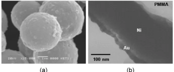
Paladent 20 used in this study is heat-polymerized PMMA resin of which physical or clinical properties are excellent. Another favorable property of PMMA resin has been

 The simplest method of storing a raster layer in the memory of the computer is using a data structure called an array..  We consider alternative methods for searching through