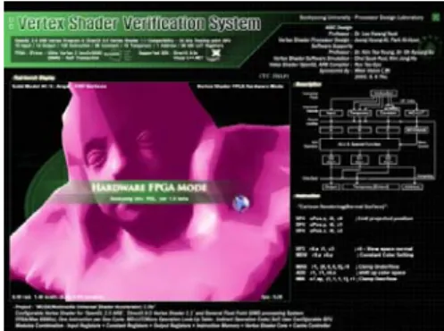
A design of a floating point unit with 3 stages for a 3D graphics shader engine
6
0
0
전체 글
(2)
(3)
(4)
(5)
(6)
수치

+2
관련 문서
This work builds inversely a base performance model of a turboprop engine to be used for a high altitude operation UAV using measured performance data,
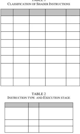
7.1 Comparison Operation Instruction 7.2 Arithmetic operation instruction 7.3 Data conversion instructions 7.4 Data transfer instructions 7.5 Data Table Operation Instruction
Unit number, baud rate and parity are entered in the Program Setting set up mode and remain in memory even if power is off.. Note that the input impedance of RS232 is 3K or
5. To enter the descaling mode, while the machine is turned on, press both the espresso and Lungo buttons for 3 seconds. Refill the water tank with the used
This book contains hundreds of complete, working examples illustrating many common Java programming tasks using the core, enterprise, and foun- dation classes APIs.. Java Examples
Frame: a single word written around the circumference of a square, in the fashion of a 'Perfect' Double Acrostic.. I have also discovered that some of the Abramelin
Process data in registers using a number of data processing instructions which are not slowed down by memory access. Store results from registers
- distributes indexes across multiple computers and/or multiple sites - essential for fast query processing with large numbers of documents - many variations:
