논문 2012-49-11-16
저전력 기법을 사용한 고해상도 오디오용 Sigma Delta Decimation Filter 설계
( Sigma Delta Decimation Filter Design for High Resolution Audio Based on Low Power Techniques )
휸 하이 아우*, 김 소 영***
( Huynh Hai Au and SoYoung Kim )
요 약
Oversampling 기법을 사용한 analog-to-digital (A/D) 컨버터에서 샘플링 된 신호의 signal bandwidth를 낮추어 주기 위해 데시메이션 필터가 사용된다. 본 논문은 sigma-delta ADC에 사용될 수 있는 저전력 4 단 32 bit 데시메이터 필터 디자인을 제 안한다. 디지털 데시메이션 필터는 CIC(cascaded integrator-comb) filter와 세 개의 half-band FIR filter로 이루어져 있다. 전 력소모를 최소화하기 위하여 CIC filter에는 pipeline구조가 사용되었고, FIR 필터의 multiplier 구조를 최적화하기 위하여 Canonic Signed Digit (CSD) 코드가 사용되었다. 130nm CMOS 공정으로 설계 자동화 CAD 도구를 사용하여 타이밍, 면적, 전력소모를 최적화하여 98.304 MHz 주파수에서 697 uW의 전력을 소모면서 32 bit, 192 kHz 아웃풋을 낼 수 있다.
Abstract
A design of a 32-bit fourth-stage decimation filter decimation filter used in sigma-delta analog-to-digital (A/D) converter is proposed in this work. A four-stage decimation filter with down-sampling factor of 512 and 32-bit output is developed. A multi-stage cascaded integrator-comb (CIC) filter, which reduces the sampling rate by 64, is used in the first stage. Three half-band FIR filters are used after the CIC filter, each of which reduces the sampling rate by two. The pipeline structure is applied in the CIC filter to reduce the power consumption of the CIC. The Canonic Signed Digit (CSD) arithmetic is used to optimize the multiplier structure of the FIR filter. This filter is implemented based on a semi-custom design flow and a 130nm CMOS standard cell library. This decimation filter operates at 98.304 MHz and provides 32-bit output data at an audio frequency of 192 kHz with power consumption of 697 μW. In comparison to the previous work, this design shows a higher performance in resolution, operation frequency and decimation factor with lower power consumption and small logic utilization.
Keywords: decimation filter, hardware implementation, audio application, semi-custom design, sigma delta decimation
* 학생회원, ** 정회원, 성균관대학교 정보통신대학 (College of Information and Communication Engineering, Sungkyunkwan University)
※ 본 논문은 2012년도 정부(교육과학기술부)의 재원으 로 한국연구재단의 기초연구사업 지원을 받아 수행 된 것임(2012-0006847).
※ 본 논문은 IDEC CAD Tool 지원을 받아 수행된 것 임.
접수일자: 2012년8월16일, 수정완료일: 2012년10월24일
Ⅰ. Introduction
Analog-to-Digital (A/D) converters that use the over-sampling technique are popular in wireless communication and audio applications because they achieve high performance in terms of accuracy, flexibility, and power consumption.
The over-sampling technique uses a sampling rate that is M times greater than the Nyquist frequency, where M is the over-sampling ratio. Decimation filters are then used to perform further filtering down to the signal bandwidth or band of interest.
In next-generation consumer audio equipment, sampling frequencies of 96, 176.4, or 192 kHz are used[1]. Single bit Sigma-Delta A/D converters use very high sampling frequencies in the range of hundreds of MHz. Therefore, decimation filters need to be used after the Sigma-Delta A/D converters in order to provide the data at a lower frequency. The task of a decimation filter is to remove the quantization noise away from the band of interest and to avoid aliasing of the high frequency components down to the low frequency region or within the signal bandwidth. The recursive algorithm structure, which is also known as the cascaded integrator-comb (CIC) filter, is widely used in comb decimator designs because it is efficient, requires no multipliers or storage elements, has a regular structure, and offers a wide range of rate changes[2].
In previous works[3~4], the decimation filter designs have 23-bit and 10-bit resolutions and decimation factors of 64 and 16. The multi-stage structure[5]
with Canonic Signed Digit (CSD) and advanced sub-expression sharing (ASS) algorithms are used to reduce the power and optimize the performance of their design. The decimation blocks in modern audio systems should have a higher decimation factor due to the higher operating frequencies.
In this research, a design of a 32-bit four-stages decimation filter operating at 98.304 MHz and output the data at an audio frequency of 192 KHz is described. The CSD and ASS algorithms are used to implement the multipliers. This approach reduces power consumption and utilizes less hardware than the conventional design by reducing the number of adders used in the design. The structure of the adder is selected to simplify the logic structure and reduce power consumption of the design. The pipeline
technique is applied to reduce the power of the design.
The paper is organized as follows. The design of the decimation filter is described in Section Ⅱ.
Section Ⅲ and Section Ⅳ present the logical and physical layout implementations and the experimental results, respectively. The conclusion is presented in Section V.
Ⅱ. Proposed Decimation Filter Design
1. Overall Filter architecture
A decimation filter performs two main operations:
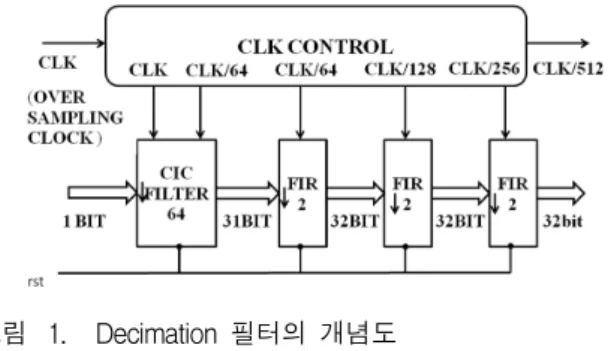
increasing the resolution as well as providing down-sampling rate. The decimation filter exchanges resolution in time for resolution in amplitude. The proposed multi-stage architecture is shown in Fig. 1.
In the first stage, a CIC filter is used to reduce the sampling rate by 64, and the others stages are 3 FIR filters, which have a total down-sampling coefficient of 8. The decimation filter operates at 98.304 MHz and provides output data at 192 kHz. The down-sampling rate of the decimation filter is 512.
To conserve space and to increase the operating frequency of this filter, all components in this design are implemented without generic multipliers.
그림 1. Decimation 필터의 개념도 Fig. 1. Decimation Filter - Block Diagram.
2. CIC filter
The transfer function of the CIC filter is given by
(1)
그림 2. CIC 모델의 구조 Fig. 2. CIC Model Structure.
where M is the decimation ratio and K is the number of stages of the integrator and comb.
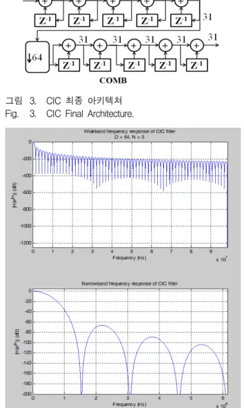
A CIC filter consists of two main sections: the cascade integrator and combs, separated by a down-sampler (Fig. 2.).
The integrator block is a cascade of K integrators with the following transfer function:
(2)
A comb block is a cascade of K combs with the following transfer function:
(3)
If the number of bits in the input data stream is
, then Eq. (4) [6] can be used to calculate , which is the most significant bit at the filter output.
(4)
As in the specification of this design, the CIC filter must use a 1-bit stream input and a down-sampling rate of 64. Therefore, the number of integrator and comb stages is 5, and the number of output bits is 31. The final structure of the CIC filter is shown in Fig. 3.
The CIC structure model is implement with MATLAB. The frequency respond of the CIC show in Fig. 4 in both wideband and narrowband.
The cascade of five integrators working at
98.304MHz and the cascade of five differentiators at 1.536MHz. This structure reduces hardware and power consumption and reduces the unwanted switching power of the CIC design. The pipelining registers at the output of fifth integrators limits the frequency of signal propagating to the comb stage.
This pipelining structure helps to save the power in CIC.
The adder which is used in the integrator of the CIC will operate at very high frequency (98.304 MHz). Therefore the 32-bit carry skip adder structure[7], with 306 total logic gates and a timing
그림 3. CIC 최종 아키텍쳐 Fig. 3. CIC Final Architecture.
그림 4. CIC 필터의 주파수 특성
Fig. 4. Frequency Response of CIC Filter.
delay of 3ns, is selected to implement the adder in CIC filter.
3. FIR filter
The second, third and fourth stage of the decimation filter is the FIR filter. The input-output signal difference equation of FIR filters can be written in the following form:
⋯
(5)
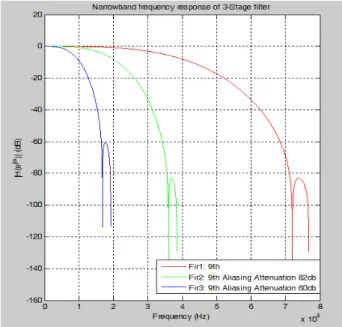
where M is the filter order, and the filter length (total number of coefficients) is M-1.The FIR filter requires a larger number of adders, multipliers, and delay elements. To reduce the power consumption in the FIR filter implementation, the 9th-order FIR filter structure is used.
The first stage of FIR filter receives the data from the output of CIC filter at 1.536MHz and provide the output data at 768kHz. The passband edge is designed at 50kHz and the maximum passband ripple is specified 0.005dB.
The second and the third stage of FIR filter are
Filter S t o p b a n d Edge
P a s s b a n d
Ripple Attenuation
FIR2 25kHz 0.05dB 80dB
FIR3 25kHz 0.05dB 60dB
표 1. FIR 필터의 특성 Table 1. FIR Filter Specification.
FIR1-2
h1 h2 h3 h4 h5
0.0026 -0.0143 -0.0338 0.1206 0.4229
h6 h7 h8 h9 h10
0.4229 0.1206 -0.0338 -0.0143 0.0026
FIR3
h1 h2 h3 h4 h5
0.0011 -0.0151 -0.0259 0.1335 0.4091
h6 h7 h8 h9 h10
0.4091 0.1335 -0.0259 -0.0151 0.0011 표 2. FIR 필터의 계수
Table 2. FIR Filter Coefficient.
design with the specification shown in Table 1.
The model of FIR filter is implemented with MATLAB, and the frequency response of 3 FIR filters are shown in Fig. 5. The fixed coefficient is used and coefficients of those FIR filters are shown in Table 2.
When fix coefficients are used in the FIR filter, the multiplication in the FIR filter will become the multiplication of a dynamic variable and a constant.
A shifter and an adder can be used to implement this multiplication so that the power consumption of the FIR filter can be reduced. The CSD [8] arithmetic is used to reduce the number of adders which are used to implement FIR filter. Then, ASS algorithm is used to share the common component in each coefficient multiplier, as a result, the total logic utilization is reduced. Before using CSD and ASS, the total number of adder in each FIR filter is 59. After CSD and ASS are applied, the total mumber of adder is reduced to 32, reducing the logic utilization by 47%.
The adders used in the last 3-stages of FIR filter stage operate at a low frequency (from 1.536MHz to 192 kHz). Therefore, the ripple carry adder structure
[7], with 288 total logic gates and a timing delay of
그림 5. FIR 필터의 주파수 특성
Fig. 5. Frequency Response of FIR Filter.
6.7ns, is selected to implement the adder in FIR filter.
4. Clock divider
There are 4 internal clocks in the decimation filter design, which are generated from the master clock (98.304 MHz) by the clock divider block. The 9-bit synchronous counter (with outputs of Register[0-8]) is used to implement the clock divider with low clock skew. The outputs of clock divider are Register[5], Register[6], Register[7] and Register[8]. The frequencies in these outputs are respectively 1536 kHz, 768 kHz, 384 kHz, and 192 kHz.
Ⅲ. Logical and Physical Implementation
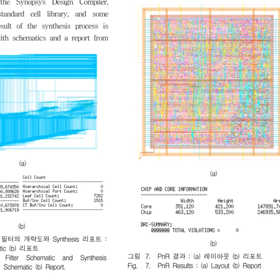
Verilog (a hardware description language) is used to describe the logic and the behavior of the proposed design. The gate-level netlist of the decimation filter design by using the Synopsys Design Compiler, Samsung 130nm standard cell library, and some constraints. The result of the synthesis process is shown in Fig. 6. with schematics and a report from
(a)
(b)
그림 6. Decimation 필터의 개략도와 Synthesis 리포트 : (a) Schematic (b) 리포트
Fig. 6. Decimation Filter Schematic and Synthesis Report : (a) Schematic (b) Report.
the Design Compiler.
After the synthesis process is complete, the Synopsys Primetime and Formality are used to do static timing analysis for the design and compare logic function between the RTL code and gate-level netlist. The Synopsys ICC is used to place and route the design. The result of the place and route process is shown in Fig. 7. During the place and route processes, the clock-tree synthesis, hold-time optimization, route optimization, and metal fill process are taken. Therefore, the final netlist after the physical implementation is changed significantly by additional buffers, metal, or other factors. Thus, the final netlist is checked again by Primetime and Formality.
A sine wave is sampled by MATLAB to create the bit stream data. A test-bench file is written using Verilog to put the bit stream to the device
(a)
(b)
그림 7. PnR 결과 : (a) 레이아웃 (b) 리포트 Fig. 7. PnR Results : (a) Layout (b) Report
그림 8. Post-layout 시뮬레이션 결과 Fig. 8. Post-layout Simulation Results.
Filter Order Decimation Factor
Opeation Freq.
(MHz)
Ouput Freq.
(MHz)
CIC 5 64 98.304 1.536
FIR1 9 2 1.536 0.768
FIR2 9 2 0.768 0.384
FIR3 9 2 0.384 0.192
표 3. 필터의 특성 결과
Table 3. Filter Performance Results.
Block Area Utilization
Ratio
Clock Divide 97.33 0.34%
CIC FILTER 6477.67 22.74%
FIR 1 7211.33 25.32%
FIR 2 7231.67 25.39%
FIR 3 7231.00 25.39%
Register buffer out 234.67 0.82%
표 4. Synthesis 특성 결과
Table 4. Syntehsis Performance Results.
under test (DUT) every 10ns. Synopsys VCS is used in RTL, and the pre-layout and post-layout simulations were performed and the results are shown in Fig. 8.
The filter performance result and the synthesis performance result of our decimation filter design are summarized in Table 3 and Table 4.
The GDS file of the design is extracted by ICC and imported into Cadence Virtuoso to conduct a DRC check using Calibre. The final step is to put the design core into the die-chip and to connect the pin to the pin of the chip. The final result is shown in Fig. 9.
Ⅳ. Experimental Results
The decimation filter design works synchronously with an external 100MHz clock. The clock tree of the design is implemented with the maximum clock skew lower than 0.6 % of the clock cycle (0.06ns). The power analysis results which are generated by
그림 9. Chip 레이아웃 사진 Fig. 9. Chip Layout Photo.
Case Freq.
MHz
Switch.
Power (mW)
Int.
Power (mW)
Leak.
Power (mW)
Total Power (mW) Best
Case 98.3 0.0576 0.399 0.0407 0.497 Worst
Case 98.3 0.0833 0.612 0.0017 0.697 표 5. 전력 분석 결과
Table 5. Power Analysis Results.
Filter Resolution Power mW
Frequency MHz
Technology nm
[3] 23 4.4 2,822 250
[9] 16 0.100 3,072 180
[10] 12 5.221 18 130
Our 32 0.697 98,304 130
표 6. 특성 비교
Table 6. Performance Comparison.
Synopsys PrimePower are provided in Table 5. The simulated performance of the proposed design is compared with other decimation filter designs of the other works and the result is showed in Table 6.
V. Conclusion
In this paper, we present the theoretical basis of a CIC decimation filter structure and its physical implementation in 130nm CMOS technology. By using the low power techniques (such as CSD, ASS, pipeline) combining with the optimal structure of adder and the retiming technique, the decimation filter designed in this work operates at 98.304 MHz and provides 32-bit output data at an audio frequency of 192 kHz with power consumption of 697 μW. In comparison to the previous work, this design shows a higher performance in resolution, operation frequency and decimation factor with lower power consumption and small logic utilization.
References
[1] Ji Kong et al., “Next-generation consumer audio application specific embedded processor,” 2010 IEEE 8th SASP, pp. 1–7, 2010.
[2] Yonghong Gao et al., “A Comparison Design of Comb Decimators for Sigma Delta Analog to Digital Converters,” Analog Integrated Circuits and Signal Processing, Volume22, Number1, pp.
51-60.
[3] Sanho Byun, Seongyoung Ryu, Youngkil Choi, Hyungdong Roh, Hyunseok Nam, and Jeongjin Roh, “Design of digital decimation filter for sigma-delta A/D converters,” The Institute of Electronic Engineers of Korea, The Institute of Electronics Engineers of Korea Semiconductor and Devices 356, pp. 34-45, Feb 2004.
[4] Young-Beom Jang, Se-Jung Yang, Sun-Kook Yoo, “Low-power Decimation Filter Structure for Sigma Delta A/D Converters in Cardiac Applications,” The Korean Institute of Electrical Engineers, The Transaction of the Korean Institute of Electrical Engineers, section 53D(2), pp 111-117, Feb 2010.
[5] K. D. Sadeghipour and A. Abbaszadeh, “Efficient realization of reconfigurable FIR filter using the new coefficient representation,” IEICE Electronics Express, Vol.8, No.12, pp. 902-907, 2011.
[6] E. B. Hogenauer, “An economical class of digital filters for decimation and interpolation,” IEEE T ASSP, vol. ASSP-29, No.2, pp. 155-162, April 1981.
[7] Min Cha et al., “Modified carry skip adder for reducing first block delay.” Proc. of the 43rd IEEE Midwest Symposium, pp. 346-348 vol.1, 2000.
[8] Hartley, R, “Optimization of canonic signed digit multipliers for filter design,” IEEE International Sympoisum on Circuits and Systems 1991, pp.
1992-1995 vol.4, 11-14 Jun 1991.
[9] Parameswaran S., Krishnapura N., “A 100 µW Decimator for a 16 bit 24 kHz bandwidth Audio ΔΣ Modulator,” Proceedings of 2010 IEEE International Symposium on Circuits and Systems (ISCAS), pp. 2410-2413, May 30 2010-June 2 2010.
[10] Jing Li; Ran Li; Ting Yi; Zhiliang Hong; Bill Yang Liu, “VLSI implementation of high-speed low power decimation filter for LTE sigma-delta A/D converter application,“ 2011 IEEE 9th International Conference on ASIC (ASICON), pp.
453-456, Oct 25-28, 2011
저 자 소 개 휸 하이 아우(학생회원)
2010년 베트남 국립 대학교, University of Science 학사 졸업.
2010년~2012년 eSilicon Corp.
2012년 성균관대학교
정보통신대학원 석사과정
<주관심분야 : SoC Design, Analog Mixed- Signal Design, Electromagnetic Compatibility>
김 소 영(정회원)-교신저자 1997년 서울대학교
전기공학부 학사 졸업.
1999년 Stanford University 전기공학과 석사 졸업.
2004년 Stanford University 전기공학과 박사 졸업.
2004년~2008년 Intel Corporation
2008년~2009년 Cadence Design Systems 2009년~현재 성균관대학교 정보통신대학 반도체시스템공학과 조교수
<주관심분야 : Device and Interconnect Modeling, Power Integrity, Signal Integrity, Computer-Aided Design, Electromagnetic Compatibility>