1V 미만 전원 전압에서 저 위상잡음에 적합한 차동 콜피츠 전압제어 발진기 회로
전만영*
A Differential Colpitts-VCO Circuit Suitable for Sub-1V Low Phase Noise Operation
Man-young Jeon
*요 약
본 논문은 1 V 미만의 전원 전압에서 저 위상잡음을 갖는 발진 신호의 발생에 적합한 차동 콜피츠 전압제 어 발진기 (VCO: Voltage Controlled Oscillator) 회로를 제안한다. 제안된 회로는 전류원으로 인덕터를 사용 함으로써 1 V 미만의 전원 전압에서 저 위상잡음의 발진을 보다 용이하게 한다. 공진기 손실을 보다 줄이기 위하여 단일 콜피츠 발진기의 두 개의 궤환 커패시터 중의 하나를 바렉터 (varactor)로 대체하였다. 0.18 μm RF CMOS 기술을 사용하는 포스트 레이아웃 (post-layout) 시뮬레이션 결과는 0.6 V에서 0.9 V 사이의 전원 전압에서 제안된 회로가 1MHz 오프셋 주파수에서 나타내는 위상잡음은 널리 알려진 교차 결합 전압제어 발 진기의 위상잡음보다 적어도 7 dBc/Hz 이상 낮음을 보여준다.
ABSTRACT
This paper proposes a differential Colpitts-VCO circuit suitable for low phase noise oscillation at the sub-1V supply voltage.
Oscillation with low phase noise at the sub-1V supply voltage is facilitated by employing inductors as the current sources of the proposed circuit. One of the two feedback capacitors of the single-ended Colpitts oscillator in the proposed circuit is replaced with the MOS varactor in order to further reduce the resonator loss. Post-layout simulation results using a 0.18 μm RF CMOS technology show that the phase noises at the 1MHz offset frequency of the proposed circuit oscillating at the sub-1V supply voltages of 0.6 to 0.9 V are at least 7 dBc/Hz lower than those of the well-known cross-coupled differential VCO.
키워드
VCO, Colpitts-VCO, Sub-1V VCO, Sub-1V oscillator
* School of Inform. and Comm. Eng. Dongyang Univ. ([email protected])
Ⅰ. Introduction
It has been predicted that the supply voltages of low-power digital circuits would reduce to 0.5V in the near future, which imposes a challenge to the
development of low-voltage RF circuits integrated
into a single silicon die together with digital
circuits [1]. Compared to the widely used CMOS
cross-coupled VCOs, NMOS or PMOS only
cross-coupled VCOs without current sources [2]-[4]
are more suitable for the sub-1V operation because they have no voltage head rooms cut down by current sources and/or their complementary MOSFETs [3]. However, they have a shortcoming that the resonator voltage swing is constrained by supply voltage V
DD[5]. This implies that phase noise performances of NMOS or PMOS only cross-coupled VCOs degrade as the power supply voltages scale down toward sub-1Vs since the phase noise is inversely proportional to the amplitude of the resonator voltage swing [5], [6].
To overcome the problem of the V
DD-constrained signal swing, the oscillators with tapped resonators, e.g. Colpitts/Clapp oscillators can be considered [5].
As a matter of fact, various differential implementations of the Colpitts/Clapp oscillators which demonstrate good phase noise performances have been presented in [7]-[11]. Most of them, however, employ the additional cross-coupled circuit stacked on the Colpitts/Clapp core connected to V
DDor ground. Thus they are not suitable for the sub-1V operation due to the voltage headroom occupied by the additional cross-coupled circuit.
In this paper, we propose a differential Colpitts-VCO circuit which excludes the additional cross-coupled stage. Thus, the proposed circuit is suitable for the sub-1V operation. The sub-1V operation is further facilitated by employing inductors as the current sources of the circuit.
Additionally, we use the MOS varactor as one of the two feedback capacitors of the single-ended Colpitts circuit in order to further reduce the resonator loss. The proposed circuit is verified through the circuit simulation using the 0.18 μm RF CMOS technology.
Ⅱ. Proposed Differential Colpitts-VCO Circuit
For the sub-1V operation, our proposed differential Colpitts-VCO circuit excludes the
cross-coupled stage as opposed to the conventional ones [9]-[10] which exploit the cross-coupled stage to boost up the tansconductance. Instead, the current source is brought back as used in the conventional Colpitts-VCO. The resultant circuit is shown in Fig. 1 (a). As shown in the figure, for the implementation of the current source, we employ the inductors (L
src1,L
src2) rather than the transistors or resistors. This leads to as high a drain-to-source and a source-to-gate bias voltage as possible at a given source supply voltage V
SSbecause the V
SSis directed to the sources of the
(a) Proposed VCO
(b) Equivalent-circuit of (a)
(c) Simulated waveform
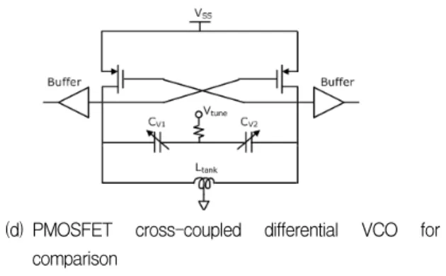
(d) PMOSFET cross-coupled differential VCO for comparison
Fig. 1 Proposed VCO and its related circuits.
transistors(M1,M2) without any dc-voltage drops between V
SSand the sources. Thus, the utilization of the inductor for the current source brings about larger source current as compared to the use of the transistor for the current source, which in turn leads to larger tansconductance thereby causing larger resonator signal swing. This nature is especially beneficial in the sub-1V operation because at the sub-1V supply voltages, the transistors acting as current sources are nearly in the triode region thereby failing to generate sufficient source currents for ensuring stable start-up of oscillation and developing such large signal swings that make phase noises low enough to be used in typical VCO applications. For the relatively high frequency region, e.g., above 3 GHz, the standard inductor in the 0.18μm RF CMOS technology can realize L
src1and L
src2since it exhibits enough impedance to carry out the function of the current source for such a high frequency region. The PMOSFETs are used to make the phase noise due to the flicker noise as low as possible.
A conventional differential Colpitts VCO with the series-tuned resonator [9] locates the varactor C
var1between the inductor L
Land the gate of M1; the varactor C
var2between the inductor L
Rand the gate of M2. However, as shown in Fig. 1 (a), our proposed VCO pushes C and C into the left
and right active part producing the negative resistances, respectively. This arrangement of C
var1and C
var2further reduces the resonator loss by the parasitic resistance values associated with the feedback capacitances replaced by C
var1and C
var2.
L
Land L
Rconstitute the resonator together with the feedback capacitances (C
L, C
R), varactor (C
var1, C
var2), and the parasitic capacitances associated with the transistors (M1, M2). L
Land L
Rhave the same inductance L
tank/2; C
Land C
Rthe same capacitance C
1; C
var1and C
var2the same variable capacitance C
var. L
Land L
Rare implemented by asymmetric spiral inductor with center tap, which has the inductance L
tank; C
Land C
Rby metal-insulator-metal capacitors; C
var1and C
var2by MOS varactors. The equivalent circuit of the Fig.1 (a) is depicted in the Fig.1 (b). R
loss1and R
loss2represent the equivalent resonator losses associated with the left and right half circuit of the Fig.1 (a), respectively. They are assumed to have the same resistance R
loss/2 due to the symmetry of the proposed VCO (R
lossdenoting the equivalent total loss of the resonator is almost determined by the loss of the symmetric spiral inductor). R
act1and R
act2represent the negative resistances of the left and right active part, respectively. They are also assumed to have the same resistance R
actdue to the symmetric structure of the left and right active part. At the steady state of oscillation, the R
loss1and R
loss2are exactly compensated by the R
act1and R
act2, respectively. Thus, the equivalent circuit is reduced to a simple L-C resonator with the inductance of L
tankand the capacitance of C
act/2 (C
actrepresents the equivalent capacitances of the left or right active part).
For a given oscillation current phasor I
oscas
shown in Fig. 1 (b), the oscillation voltage phasor
V
g1and V
g2at the node 1 and 2 are given by
V
g1=jI
osc/(ωC
act) and V
g2=-jI
osc/(ωC
act), respectively,
which means that V
g1, the gate voltage of M1
shown in Fig.1 (a) is exactly in 180 degree
out-of-phase from V
g2, the gate voltage of M2.
Indeed, the simulated waveforms of V
g1and V
g2shown in Fig.1 (c) indicate that they are exactly in 180 degree out-of-phase from each other, i.e., they behave in the differential mode. A PMOS cross-coupled VCO mentioned in the next section for comparison with the proposed VCO is shown in Fig. 1 (d). It employs the exactly same inductor L
tankas the proposed VCO for comparison.
Ⅲ. Comparisons of Proposed and Cross-coupled VCO
The post-layout simulated amplitudes of the oscillation voltages of the proposed VCO and PMOS cross-coupled VCO in Fig. 1 (d) change with supply voltages V
SSas shown in Fig. 2(a).
For possibly valid comparison, we use same inductors L
tankfor the implementation of the resonators of both VCOs, and tune both VCOs at the same frequencies. For L
tank=3.31 and 2.14 nH, the amplitudes of the proposed VCO for various supply voltages are always much larger (about 1.5 to 1.7 times larger) than those of the cross-coupled VCO. From the figure, we observe that for a given
(a) Comparison of amplitudes of oscillation voltage
(b) Comparison of phase noises
(c) Comparison of power consumptions
(d) Chip layout of proposed-VCO
Fig. 2 Comparisons of proposed and cross-coupled VCO.
supply voltage V
SS, the oscillation amplitude of the
cross-coupled VCO is actually limited by the supply
voltage in accordance with our expectation, whereas
proposed VCO swings with much larger amplitude
than the supply voltage. For both of L
tank=3.31 and
2.14 nH, this leads to about -6 dBc/Hz lower phase
noises of the proposed VCO than those of the
cross-coupled VCO as shown Fig.2 (b). Figure 2
(b) also shows that the proposed VCO can oscillate
[2] [4] [12] [13] [14] [15]
(sim.) This (sim.) Tech.(μm) 0.18 0.09 0.13 0.18 0.18 0.13 0.18
Freq.
(GHz) 1.4 3.55 3.58 5.45 8.5 5.2 5.64 Supply Volt.
(V) 0.35 0.22 0.3 0.6 0.7 0.5 0.6
PN@1Mhz
(dBc/Hz) -129 -112.97 -116.88 -111.5 -121.6 -117 -123.3
PDC (mW) 1.46 0.33 0.225 6.9 6 2 4.43 FOM
(dBc/Hz) -190 -188.79 -194.43 -177.8 -190 -188 -191.8
Tuning
Range (%) 2.97 5.1 20.4 27.2 4.7 11.2 7.5
Table 1. Performance comparison with previous
reports with the phase noise of -108.7 dBc/Hz for
L
tank=3.31nH and -103.3 dBc/Hz for L
tank=2.14 nH at 1 MHz offset frequency even at the supply voltage of 0.2 V, whereas the cross-coupled VCO ceases to oscillate at the supply voltages lower than 0.6 V.
For the two different inductors, Fig. 2 (c) compares the power consumptions of the proposed VCO with those of the cross-coupled VCO. The figure indicates that for a given supply voltage, the proposed VCO consumes much more power than the cross-coupled VCO (this is one of well-known characteristics of Colpitts oscillators). The figure of merit (FoM) of the proposed VCO are in the range of -190.3 to -191.8 dBc/Hz for the supply voltages of 0.3 to 1 V. They are slightly lower than but actually same as those of the cross-coupled VCO since the lower phase noises of the proposed VCO compared to those of the cross-coupled VCO are cancelled by the higher power consumptions of the proposed VCO. The gate bias voltages Vbias of the proposed VCO at the given supply voltages are adjusted to develop two to three times larger negative resistances Ract than the half of the inductor loss Rtank in order to ensure stable start-up of oscillation. For the inductors of L
tank=3.31 and 2.14 nH, the oscillation frequencies of both VCOs have been tuned at about 5.6 and 6.6 GHz, respectively. The values of C
L(=C
R) and C
var1(=C
var2) used for the simulation of the proposed VCO have been about 563.2 and 751.6 fF, respectively. The proposed, and cross-coupled VCO have the transistor sizes of 200 μm/0.18 μm, and 100 μm/0.18 μm, respectively. Figure 2 (d) shows the layout of the proposed VCO which ocupies the area of 0. 9×1.4 mm
2.
The performance comparisons of the proposed VCO and other previously reported VCOs using sub-1 V supply voltages are summarized in Table 1. From the table, we notice that the phase noise performance of the proposed VCO for VSS=0.7V is remarkable among the results reported for the
VCOs with sub-1V supply voltages and the center frequencies above 3 GHz. We also notice that FoM of the proposed VCO is comparable to the results reported thus far.
Ⅳ. Conclusions
A differential Colpitts-VCO circuit suitable for low phase noise oscillation at sub-1V supply voltages has been proposed. The sub-1V oscillation is facilitated by employing inductors as the current sources. The post-layout simulation result reveals that the proposed VCO exhibits much larger resonator signal swings than the PMOS only cross-coupled VCO at the sub-1V supply voltages.
This causes the proposed VCO to have much lower
phase noises at the sub-1V supply voltages as
compared to the cross-coupled VCO. However, the
proposed VCO consumes much more power than
the cross-coupled VCO. Thus, the proposed VCO is
more suitable for the applications in which
stringent phase noise performance at the sub-1V
supply voltages is required, but power consumption
is not so important. The post-layout simulated
phase noise performance of the proposed VCO at
sub-1V supply voltage is remarkable compared to
the results reported for the VCOs with sub-1 V
supply voltages and the center frequencies above 3 GHz. FoM of the proposed VCO is comparable to the results reported for the VCOs with sub-1 V supply voltage.
References
[1] F. Yamashita, T. Matsuoka, T. Kihara, I.Takobe, H.-J. Park, and K. Taniguchi, “Analytical design of a 0.5V 5GHz CMO SLC-VCO,” IEICE Electronics Express, vol. 6, no. 14, pp. 1025-1031, 2009.
[2] K. Kwok and H. C. Luong, “Ultra-low-voltage high-performance CMOS VCOs using transformerfeedback,” IEEE J. Solid-State Circuits, vol.40, pp. 652-660, 2005.
[3] D. Park and S. Cho, “A power-optimized CMOS LC VCO with wide tuning range in 0.5-V supply,” in Proc. IEEE ISCAS 2006, Island of Kos, Greece, pp. 3233-3236, 2006.
[4] S.-L. Jang, C.-J. Huang, C.-C. Liu, and C.-W.
Hsue, “A 0.22 V quadrature VCO in 90 nm CMOS process,” IEEE Microw. Wireless Compon.
Lett., vol. 19, no. 9, pp. 566-568, 2009.
[5] T. H. Lee and A. Hajimiri, “Oscillator phase noise: a tutorial,” IEEE J. Solid-State Circuits, vol.
SC-35, no. 3, pp. 326-336, 2000.
[6] N. Itoh, “Low voltage low phase noise CMOS VCO and its Flicker noise influence,” IEICE Trans. Electron., vol. E86-C, no. 6, pp. 1062-1068, 2003.
[7] R. Aparicio and A. Hajimiri, “A noise-shifting differential Colpitts VCO,” IEEE J. Solid-State Circuits, vol. SC-12, no. 12, pp. 1728-1736, 2002.
[8] M.-D. Tsai, Y.-H. Cho, and H. Wang, “A 5-GHz low phase noise differential Colpitts CMOSVCO,”
IEEE Microw. Wireless Compon. Lett., vol. 15, no. 5, pp. 327-329, 2005.
[9] S.-L. Jang, Y.-J. Song, and C.-C. Liu, “A differential Clapp-VCO in 0.13 μm CMOS technology,” IEEE Microw. Wireless Compon. Lett., vol. 19, no. 6, pp. 404-406, 2009.
[10] J.-P. Hong and S.-G. Lee, “Low phase noise Gm-boosted differential gate-to-source-feedback Colpitts CMOS VCO,” IEEE J. Solid-State Circuits, vol. SC-44, no. 11, pp. 3079-3091, 2009.
[11] J.-A. Hou and Y.-H. Wang, “A 7.9 GHz low-power PMOS Colpitts VCO using the gate
inductive feedback,” IEEE Microw. Wireless Compon. Lett., vol. 20, no. 4, pp. 223-225, 2010.
[12] S.-L. Jang, C.-J. Huang, C.-W. Hsue, and C.-W.
chang, “A 0.3 V cross-coupled VCO using dynamic threshold MOSFET,” IEEE Microw.
Wireless Compon. Lett., vol. 20, no. 3, pp. 166-168, .2010.
[13] M.-T. Hsu and H.-J. Li, “Design of high performance and wide-band VCO with tran- sformer feedback,” in Proc. APMC 2008, Hong Kong and Macau, China, pp. 1-4, 2008.
[14] C.-H. Chang and C.-Y. Yang, “A low-voltage high-frequency CMOS LC-VCO using a transformer feedback,” in Proc. IEEE RFIC Symp.
2008, Atlanta, Georgia, USA, pp. 545-548, 2008.
[15] B. Catli and M. M. Hella, “A 0.5-V 3.6/5.2 GHz CMOS multi-band LC VCO for ultra low-voltage wireless applications,” in Proc. IEEE ISCAS 2008, Seattle, WA, USA, pp. 996-999, 2008.
저자 소개
전만영(Man-young Jeon)