Optimal Determination of the Fabrication Parameters in Focused Ion Beam for Milling Gold Nano Hole Array
Eun Byurl Cho
a,b, Hee Min Kwon
a, Hee Sun Lee
b, and Jong-Souk Yeo
a,b*
a
School of Integrated Technology, Yonsei University, Incheon 406-840
b
Yonsei Institute of Convergence Technology, Yonsei University, Incheon 406-840
(Received July 25, 2013, Revised August 21, 2013, Accepted August 22, 2013)
Though focused ion beam (FIB) is one of the candidates to fabricate the nanoscale patterns, precision milling of nanoscale structures is not straightforward. Thus this poses challenges for novice FIB users. Optimal determination in FIB parameters is a crucial step to fabricate a desired nanoscale pattern. There are two main FIB parameters to consider, beam current (beam size) and dose (beam duration) for optimizing the milling condition. After fixing the dose, the proper beam current can be chosen considering both total milling time and resolution of the pattern. Then, using the chosen beam current, the metal nano hole structure can be perforated to the required depth by varying the dose. In this experiment, we found the adequate condition of 0.1 nC/μm
2dose at 1 pA Ga ion beam current for 100 nm thickness perforation.
With this condition, we perforated the periodic square array of elliptical nano holes.
Keywords : Focused Ion Beam (FIB), Nano hole array, Nano fabrication
I. Introduction
Nanoscale structures can potentially be used for various applications, such as biosensors [1], solar cells [2,3], 3-D structures [4,5], plasmonic arrays [6-10], nano-optical filters [11-13], micro electro mechanical systems structures [14], and honeycomb structures [15]. There are several techniques for nano structure fabrication such as photolithography, elec- tron beam lithography. Conventional photolithography such as ArF photolithography, is limited in its reso- lution due to Abbe diffraction limit [16]. Electron beam lithography can provide finer resolution but it requires several steps of spin coating, developing,
and etching. Hence it may not be suitable for certain nanostructure applications. To overcome these limi- tations in nano prototyping techniques, the direct patterning based on focused ion beam (FIB) has gained an interest from researchers studying nano scale devices [17]. Although FIB has difficulties in both large area fabrication and throughput, nano- structure mold fabricated by FIB can further be used with roll-to-roll nanoscale imprinting for scalable nanofabrication processes [18].
3-D schematics of general FIB structure drawn
with Rhino design tool is shown in Fig. 1 to help un-
derstanding of the conventional beam path from met-
al ion source to sample when operating the FIB in-
Figure 1. Schematics of ion beam column showing the beam path in general FIB [19].
strument [19]. Usually FIB uses the liquid metal ion source (LMIS) to generate the ion [20], because melt- ed metal provides small metal tip for high resolution.
And among several metallic elements, gallium (Ga) is typically used because of its low melting temperature (29.8
oC) [21]. So liquid Ga metal is ionized by apply- ing an extraction voltage and suppressor controls the extracted Ga ions by oppositely applying the voltage.
Then the generated Ga ions are accelerated by an ac- celerating voltage within the ion column and the condenser lens concentrates the beam on a small size.
Then apertures cut the concentrated beam and beam blanker blocks the ion beam during the FIB operation.
Octopole controls the shape of the beam to achieve a good quality of beam. Then, objective lens is focusing the concentrated beam on the sample to perforate [20].
Among every part in FIB column, condition of fab- rication mainly depend on the aperture and beam blanker while other parts are mainly serving to focus the beam so they can remain fixed once they are optimized.
Beam current directly correlates to a beam size be- cause an aperture reduces the number of the accel- erated ions that are counted by a Faraday cup. Thus the value is presented with a unit in current but it is practically regarded as a beam size.
Dose indicates the amount of time exposing the unit area so it correlates with a total milling time.
The unit of dose in nC/μm
2means that ions reach the surface per unit area for a total fabrication time. The dose can be given as,
×
×
where I is the ion beam current, T is the processing time, and A is the size of the process area. Finding a proper beam size can be achieved by varying the beam current at a fixed dose.
Various research outcomes on FIB have been sum- marized in a book edited by L. A. Giannuzzi et al.
[20]. However they mainly focus on the fabricated structures without providing detailed guidance on utilization of focused ion beam so the operational challenges to achieve required milling results still remain to the individual practice of a user. In this paper, we present two main FIB fabrication parame- ters to consider and explain the principle of control- ling these parameters to facilitate FIB based nano- scale research.
II. Experiments
For the fabrication of the metallic nano hole ar- rays, a sample of gold film sputtered on glass sub- strate was prepared first and then, relevant nano patterns were milled on the sample by using FIB.
There are two major fabrication parameters to de- termine optimal milling condition in FIB process, beam current and dose. Between the two parameters, one was fixed while controlling the other parameter.
In this paper, fabrication of a metallic nanostru- cture or nano hole array was carried out on the gold film using a dual beam FIB machine (JEOL, JIB-4601F).
This dual beam design has an advantage of minimiz-
Table 1. Major specification of FIB (JEOL JIB-4601F).
Ion source Ga liquid metal source Accelerating voltage 1 to 30 kV
Magnification ×100 to ×300,000 Image resolution 5 nm (at 30 kV) Beam current Up to 60 nA (at 30 kV)
ing sample damage from the Ga ion gun by reducing the ion beam exposure time on a sample. Table 1 shows a major specification of FIB instrument we used in this experiment. The pattern can be drawn with the combination of spot, rectangle, and line or in the format of BMP file. The emission current is re- lated to the resolution but low emission current means that beam current may not be stable. There- fore the extraction voltage in the instrument is con- figured automatically to extract a fixed emission cur- rent value of 2.0 μA. This extraction voltage is the field emission energy to break the bond of the melted Ga so that the Ga ions can be emitted from the source [22]. And the acceleration voltage is fixed to 30 kV.
1. Sample preparation
In this experiment, 1 inch-size glass substrate with 700 μm in thickness was prepared using a DC sputtering deposition tool (SNTEK). Before sputtering gold on to the glass, the substrate was cleaned using acetone, IPA, and DI water in ultrasonic bath for 5 minutes, respectively. We prepared the 100 nm thick gold film by sputtering for 125 seconds at a working pressure of 3 mTorr of 30 sccm Ar gas and a DC pow- er of 300 W. Thickness of the sputtered gold film was proportional to a deposition time.
2. Fabricating parameters: beam current and dose
To find the independent effect of beam current on fabricated hole size and optimize the magnitude of beam current for perforating the 100 nm size of
holes, experiment is processed by varying the beam current such as 1, 3, 10, 30, 50, and 100 pA when a dose is fixed as 0.1 nC/μm
2.
To find the effect of another fabricating parame- ter, dose, experience is provided. Optimized condition for nanostructure fabrication can be found by com- paring the doses of 0.02, 0.1, 0.2, and 0.3 nC/μm
2at a fixed beam current of 1 pA.
III. Results and Discussion
There are several factors to consider when operat- ing the FIB. Before taking other fabrication parame- ters into account for milling process, the ion beam in FIB needs to be focused first in order to generate a result with expected resolution. Since a beam that is out-of-focus does not efficiently perforate at the surface of the sample, resulted pattern may not turn out to be same as planned.
For the voltages used in the formation of the beam,
extraction voltage induces the liquid metal to gen-
erate a Ga ion. Then the acceleration voltage affects
the velocity of the ion that moves within the ion
column. While we can still detect the surface image
for the ions with low acceleration voltage and corre-
sponding low energy, high acceleration voltage pro-
vides sufficient energy to generate more secondary
ions after collision so the image quality can be im-
proved. Following the acceleration process, the ions
are then reduced in size by various apertures that
control the intensity or the number of the ions. These
apertures can equivalently be regarded as beam cur-
rents or beam sizes. Using the smaller size of the
beam or the aperture, we can enhance the resolution
but can increase processing time or dose to machine
the required depth. The dose can be practically con-
sidered same as the milling time of the pattern. For
determining the optimal condition, both size and
depth of a hole are adjusted by beam current and
Figure 2. The SEM image of the nano holes produced by using different beam current from 1 pA to 100 pA at a dose of 0.1 nC/μm
2.
-10 0 10 20 30 40 50 60 70 80 90 100 110 0
50 100 150 200 250 300 350 400 450 500
Meas ured hole size (nm)
Beam current (pA)
Figure 3. The graph shows the relationship between hole size and beam current.
Table 2. The measured nano hole sizes according to the beam current at a dose of 0.1 nC/μm
2. Beam current Measured hole size
(a) 1.00 pA 85 nm
(b) 3.00 pA 133 nm
(c) 10.00 pA 200 nm
(d) 30.00 pA 256 nm
(e) 50.00 pA 300 nm
(f) 100.00 pA 456 nm
dose, at the same time. However, to evaluate the ef- fect of beam current on size and effect of dose on depth, separate experiments are conducted at section 3.1 and 3.2, independently. Therefore FIB user can choose the beam current and dose based on the data from this paper.
1. The effect of beam current for fabricating nano hole array using FIB
We fix the dose to 0.1 nC/μm
2and continuously change the beam current from 1.00 pA to 100.00 pA.
As discussed before, increased beam current results in larger size of the perforated spot. The important thing before perforating the pattern is to focus the beam on the surface and to adjust its shape to a circle by correcting the stigma of the beam. A distorted shape of the beam can not perforate the structure as drawn in the original pattern. The FIB tool of our in- terest has the thirteen different apertures in size and the measured hole size according to some of different beam current are shown in Table 2. Fig. 2 shows the
SEM images of the hole sizes fabricated using the beam current from 1.00 pA to 100.00 pA.
The relationship between the hole size and the beam current is presented in Fig. 3 based on the data from Table 2. In this experiment, beam current of 1 pA is chosen to perforate the 100 nm size of the hole. Beam current of 3 pA produces excessively large hole than the size of the original pattern and it potentially ex- poses more to Ga ion damage. Therefore, beam current of 1 pA is proper to perforate the 100 nm sized hole.
2. The effect of dose for fabrication nano hole ar- ray using FIB
After finding a proper beam size, we fix a beam
current to 1 pA and vary the dose from 0.02, 0.1, 0.2,
to 0.3 nC/μm
2to identify a proper dose. By observ-
ing the cross-sectional image of four different doses
Figure 4. The top and cross-sectional view of 200 nm nano circle hole perforated on 100 nm thick- ness of gold layer at four different doses us- ing 1 pA of beam current. (a) 0.02 nC/μm
2dose, total milling time is 1 seconds (sec), resultant hole depth is 73 nm, (b) 0.1 nC/μm
2dose, 5 sec, 132 nm, (c) 0.2 nC/μm
2dose, 9 sec, 155 nm, (d) 0.3 nC/μm
2dose, 15 sec, 187 nm.
Figure 6. The profile of the hole perforation at 0.1 nC/μm
2dose with different beam current, (a) 1 pA (angle of the slope is 83
o), (b) 3 pA (77
o), (c) 10 pA (64
o), (d) 30 pA (69
o).
2μm
Figure 7. FE-SEM images of surface plasmon reso- nance nanostructures perforated by FIB on gold film on the glass substrate (An array of 15×20 square holes with major and minor axis of 200 nm and 100 nm, respectively with a dose of 0.1 nC/μm
2and beam current of 1pA).
0.0 0.1 0.2 0.3
50 100 150 200
Dep th (nm)
Dose (nC/ μ m
2)
100 nm thick of gold
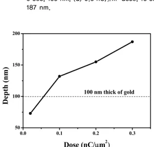
Figure 5. The graph shows the relationship between the milling depth and dose.
shown in Fig. 4, we can determine an optimal con- dition for perforation. In Fig. 4, to determine the op- timal dose for perforating 100 nm in depth, 200 nm size nano hole is used instead of 100 nm size hole, because size of hole is not a concerned parameter.
Analysis of depth vs. dose is shown in a graph in Fig.
5. Milling with a dose of 0.02 nC/μm
2is under per- forated (Fig. 4(a)) and a dose of 0.2 nC/μm
2is clear- ly over perforated (Fig. 4(c)). Therefore 0.1 nC/μm
2is determined to be a suitable dose for milling 100 nm
thick gold metal film.
Cross-sectional image of the perforated shape is shown in Fig. 6 and is analyzed by measuring the slope of the edge of the perforated hole. This figure shows that the lower beam current can perforate the hole perpendicularly at dose of 0.1 nC/μm
2. The beam with the lower current possesses more ions having perpendicular direction as the beam is limited by the size of the aperture.
With determined optimal fabrication condition, we
perforate the square array of nanoscale elliptical
holes having 100 nm and 200 nm in diameter on the
100 nm thickness of gold film utilizing this condition.
As shown in Fig. 7, it takes about 20∼30 minutes to fabricate an array of 15×20 square holes on the gold film with the dose of 0.1 nC/μm
2and beam current of 1 pA. By using this optimally determined milling condition in focused ion beam, we demonstrated the fabrication of the desired nanoscale hole arrays for surface plasmonic nanostructures as shown in Fig. 7.
IV. Conclusion
Nanoscale hole arrays are fabricated on the gold film by optimizing the ion beam condition using an FIB instrument. Among the various parameters in FIB, the beam current sets the resolution of the pat- tern and the dose determines the depth of the perfo- rated pattern. According to the experiment, the dose of 0.1 nC/μm
2and the beam current of 1 pA are pro- ven to be an adequate condition to mill an array of ellipses having the major and the minor axis of 200 nm and 100 nm, respectively, for the 100 nm thick gold film. By referring to the data in this experiment, FIB user can choose a proper condition of beam cur- rent and dose according to the size and depth of the desired nanostructures.
Acknowledgments
This research was supported by the MSIP (Ministry of Science, ICT and Future Planning), Korea, under the “IT Consilience Creative Program” (NIPA-2013- H0203-13-1002) supervised by the NIPA (National IT Industry Promotion Agency).
References
[1] B. Schiedt, L. Auvray, L. Bacri, G. Oukhaled, A.
Madouri, E. Bourhis, G. Patriarche, J. Pelta, R.
Jede, and J. Gierak, Microelectron. Eng. 87, 1300 (2010).
[2] H. W. Shin, J. C. Chin, H. J. Kim, S. Kim, and J. W. Choi, J. Korean Vac. Soc. 22, 3 (2013).
[3] Y. H. Ko, M. S. Kim, and J. S. Yoo, J. Korean Vac. Soc. 21, 4 (2012).
[4] M. J. Vasile, Z. Niu, R. Nassar, W. Zhang, and S. Liu, J. Vac. Sci. Technol. B 15, 2350 (1997).
[5] C. H. Chao, S. C. Shen, and J. R. Wu, J. Materials Eng. and Performance 18, 878 (2009).
[6] D. S. Kim, Q. H. Park, S. H. Han, and Ch. Lienau, J. Korean Vac. Soc. 12, S1 (2003).
[7] J. Elliott, I. I. Smolyaninov, N. I. Zheludev, and A. V. Zayats, Optics letters 29, 1414 (2004).
[8] A. Krishnan, T. Thio, T. J. Kim, H. J. Lezec, T.
W. Ebbesen, P. A. Wolff, J. Pendry, L. Martin- Moreno, and F. J. Garcia-Vidal, Optics Communi- cations 200, 1 (2001).
[9] A. Degiron, H. J. Lezec, W. L. Barnes, and T. W.
Ebbesen, Applied Physics Letters 81, 4327 (2002).
[10] H. F. Ghaemi, T. Thio, D. E. A. Grupp, T. W.
Ebbesen, and H. J. Lezec, Physical Review B 58, 6779 (1998).
[11] D. Inoue, A. Miura, T. Nomura, H. Fujikawa, K.
Sato, N. Ikeda, D. Tsuya, Y. Sugimoto, and Y.
Koide, Appl. Phys. Lett. 98, 093113 (2011).
[12] Q. Chen and D. R. S. Cumming, Opt. Express 18, 14056 (2010).
[13] Y. S. Do, J. H. Park, B. Y. Hwang, S. M. Lee, B. K. Ju, and K. C. Choi, Adv. Optical Mater. 1, 133 (2013).
[14] J. Matovic, J. Kettle, E. Brousseau, and N. Ada- movic, PROC. 26th In Proc. 26th Internat. Conf.
on Microelectronics (MIEL) 1, 104 (2008).
[15] H. Hosokawa, K. Shimojima, Y. Chino, Y. Yamada, C. E. Wen, and M. Mabuchi, Mater. Sci. Eng.
A344, 365 (2003).
[16] S. H. Kim, H. D. Kim, S. H. Lee, C. M. Park,
M. H. Ryoo, G. S. Yeo, J. H. Lee, H. K. Cho,
W. S. Han, and J. T. Moon, Proc. of SPIE 5376,
1082 (2004).
[17] J. Gierak, D. Mailly, G. Faini, J. L. Pelouard, P.
Denk, F. Pardo, J. Y. Marzin, A. Septier, G.
Schmid, J. Ferré, R. Hydman, C. Chappert, J.
Flicstein, B. Gayral, and J. M. Gérard, Microele- ctronic Engineering 57, 865 (2001).
[18] D. Angmo, S. A. Gevorgyan, T. T. Larsen-Olsen, R. R. Sondergaard, M. Hosel, M. Jorgensen, R.
Gupta, G. U. Kulkarni, and F. C. Krebs, Organic
Electronics 13, 984 (2013).
[19] S. Reyntjens and R. Puers, J. Micromech. Microeng.
11, 287 (2001).
[20] Lucille A. Giannuzzi and F. A. Stevie, Introduc- tion to Focused Ion Beams, (Springer, 2005).
[21] K. Y. Kim, Plasmonics - Principles and Appli- cations, (InTech, 2012).
[22] D. N. Zurlev and R. G. Forbes, J. Phys. D: Appl.
Phys. 36, L74 (2003).
금 나노홀 어레이 제작을 위한 집속 이온빔의 공정 최적화
조은별a,bㆍ권희민aㆍ이희선bㆍ여종석a,b*
a
연세대학교 글로벌융합공학부, 인천 406-840
b
![Figure 1. Schematics of ion beam column showing the beam path in general FIB [19].](https://thumb-ap.123doks.com/thumbv2/123dokinfo/5381182.410630/2.892.126.394.137.382/figure-schematics-beam-column-showing-beam-path-general.webp)