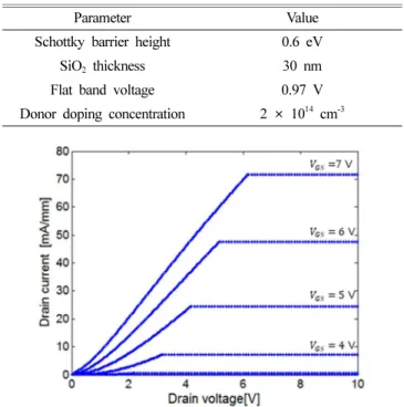
is changed by the gate oxide thickness and Schottky barrier height, but it is hardly changed by the doping concentration. For a GaN SB MOSFET with ITO source and drain electrodes, the calculated threshold voltage was 3.5 V which was similar to the measured value of 3.75 V and the calculated drain current was 1.2 times higher than the measured.
Keywords: Schottky barrier, UV sensor, thermionic emission, MOSFET, gallium nitride.
1. INTRODUCTION
Gallium nitride and related devices have been studied due to its excellent material properties such as high breakdown voltage, high mobility, high velocity saturation and wide bandgap, which are more than suitable for high frequency power devices [1,2].
There have been various GaN based transistors, such as hetero- junction field-effect transistors (HFET) [3] and high electron mobility transistors (HEMT) [4], etc. GaN Schottky barrier MOSFET has low off-state current, because it has high hole barrier which prevent the leakage current. And GaN-based Shottky-Barrier MOSFET can be used for the active pixel sensor (APS) type UV image sensor by integration with a Scottky electrode based GaN UV photodiode [5]. So it becomes miniaturized than the existing UV sensor by using the Si-based circuit and GaN MSM UV Sensor. There has been a work to model GaN SB-MOSFET by fitting the data that is obtained from the TCAD simulation to the experimental data [7].
In this work, the drain current of the SB MOSFET was modeled mathematically by considering thermionic emission and tunneling
components was calculated for accumulation mode. The electron concentration was substituted by the channel electron concentration for modeling the thickness of depletion layer below the schottky contact, because the barrier width is changed by it.
The pinch-off voltage was considered. Also a simple mathematical model of drain current was developed by using quantum model. The calculated drain current was close to the measured value of the experimental data.
2. MODELING
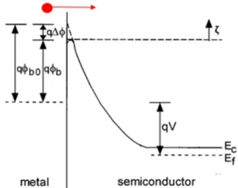
Fig. 1 (a) shows an implementation example of the Schottky barrier MOSEFT fabricated on a high-resistive n-type GaN substrate using ITO as electrodes for source and drain. Fig. 1 (b) and (c) show the energy band diagram of a metal-semiconductor contact and channel electron concentration with variation of gate voltage. The tunneling current is suppressed by the thick Schottky barrier in equilibrium i.e. no gate bias as shown in Fig. 1 (a).
But the channel electron concentration increases by an increased positive gate voltage, so as to increase the diffusion current. For the drift current is exactly same with the diffusion current in a quasi-equilibrium condition, the electric field increases accordingly, which makes the energy band sharper in slope and the narrower in width as shown in Fig. 1 (b).
If a drain voltage is applied in this condition, tunneling current can be flowed through the thinner Shottky barrier width. The channel electron concentration N
chis
School of Electronics Engineering, College of IT Engineering, Kyungpook National University, Daegu 702-701, Korea.
+
Corresponding author: [email protected]
(Received: Jan. 23, 2017, Revised: Mar. 16, 2017, Accepted: Mar. 17, 2017)
This is an Open Access article distributed under the terms of the Creative Commons Attribution Non-Commercial License(http://creativecommons.org/
licenses/bync/3.0) which permits unrestricted non-commercial use, distribution,
and reproduction in any medium, provided the original work is properly cited.
(1)
(2)
(3)
where W is the Schottky barrier width, is the tunneling probability.
2.1 Thermionic emission
At the source junction, a reverse biased Schottky contact, there are two major current components: thermionic and tunneling emission. Fig. 2 shows the energy band diagram of a Schottky contact at the reverse bias and electrons flow from the metal over
the energy barrier into the semiconductor. Thermionic emission can be expressed by [7]
(4)
where is the quantum transmission coefficient of the electron above the effective Schottky barrier height, is the Richardson constant. Assuming no significant loss in the process, thermionic emission can be expressed by integrating Eq. (5).
(5)
2.2 Tunneling
Fig. 3 presents the energy band diagram of the reverse biased metal semiconductor junction, and defines relevant
(7) where is the effective mass, η and W(η) are the Shottky barrier height and width for the tunneling electron, as shown in Fig. 3. In this work, W(η) was modeled by approximating the conduction band to a triangular shape and using the ratio,
(8) where is the Schottky barrier width for a reversely biased condition [9].
Tunneling probability can be expressed by substituting Eq. (8) into Eq. (7)
T ( ) η
T ( ) ζ
A∗
m∗
W qV (
b) Fig. 1. Schematic cross-section of SB MOSFET(a), whose energy
band diagram showing channel electron concentration at low gate voltage(b), and high gate voltage(c).
Fig. 2. Schematic conduction band diagram of a reversely biased
metal-semiconductor contact: electrons flow from the metal
into the semiconductor over the energy barrier.
(9)
can be approximated as , because is very small in GaN. The Schottky barrier width is changed by the channel electron concentration . Tunneling current density of the SB MOSFET can be expressed by
(10)
The lowering of the Schottky barrier height, is typically expressed
(11)
where is the surface field which is the slope of the energy band.
(12) Eq. (12) can be modified to Eq. (13), because the schottky barrier width is changed by the channel electron concentration.
(13)
Schottky barrier lowering equation of the SB MOSFET can be found by substituting Eq. (13) into Eq. (11).
(14)
where is all the substrate charge present in the n-type substrate expressed by [10]
(17)
Because is dominant compared with other terms in the accumulation region, can be simplified.
(18)
As you can see in Fig. 4, is very small in the accumulation region when using the n-GaN substrate, because almost gate voltage is applied to the . So Eq. (16) can be modified to the Eq. (24).
(19)
Channel electron concentration is expressed finally by
(20)
2.4 Drain current at accumulation mode SB MOSFETs
Drain current equation is expressed
(21) where and W are the channel thickness and width respectively, is the drain current density composed of
qV
bq∅
b+ qV qV
nW qV (
b) N
chΔ∅
E
sW
depQ
sube
q∅s ---kT
Q
sub∅
sV
oxV
gV
fb2 ε
skTN
de
q∅s ---kt