A Pulser System with Parallel Spark Gaps at High Repetition Rate
Byung-Joon Lee*, Jong Woo Nam*, Hasibur Rahaman*, Sang Hoon Nam*★
Jae Woon Ahn**, Seung Whan Jo**, Hae Ok Kwon**
Abstract
A primary interest of this work is to develop an efficient and powerful repetitive pulser system for the application of ultra wide band generation. The important component of the pulser system is a small–sized coaxial type spark gap with planar electrodes filled with SF6 gas. A repetitive switching action by the coaxial spark gap generates two consecutive pulses in less than a microsecond with rise times of a few hundred picoseconds (ps). A set of several parameters for the repetitive switching of the spark gap is required to be optimized in charging and discharging systems of the pulser.
The parameters in the charging system include a circuit scheme, circuit elements, the applied voltage and current ratings from power supplies. The parameters in the discharging system include the spark gap geometry, electrode gap distance, gas type, gas pressure and the load. The characteristics of the spark gap discharge, such as breakdown voltage, output current pulse and recovery rate are too dynamic to control by switching continuously at a high pulse repetition rate (PRR). This leads to a low charging efficiency of the spark gap system. The breakthrough of the low charging efficiency is achieved by a parallel operation of two spark gaps system. The operational behavior of the two spark gaps system is presented in this paper. The work has focused on improvement of the charging efficiency by scaling the PRR of each spark gap in the two spark gaps system.
Key words: Spark gap, microplasma discharge, high repetition rate, charging efficiency, ultra-wideband application.
* Pohang Accelerator Laboratory POSTECH
*★ Corresponding author
** Hanwha Corporation Gumi Plant, R & D Department 2
Manuscript received Nov.21,2011;Revised Dec.14, 2011 Accepted Dec. 15. 2011
I. Introduction
There are two distinct approaches to the development of high power ultra wideband system [1]. The first approach involves a system run by high powered devices, that includes high pressure spark gap switches, with breakdown voltage at several 100 kV’s to a few MV’s and ultrafast switching technique [2-3]. These switches generate a high power fast-rise-time pulse which contains the high frequency components of the resulting spectrum.
The overall system becomes bulky and results in a significant complexity and increased cost. In addition, the
gas dynamic processes, like deionization of the ionized species and subsequent cooling of the hot gas, are adversely affected at high energy transfer, thus limiting the PRR of the spark gaps to a few kHz even after employing external cooling.
The second approach or the more recent approach involves the ultra wideband system run by low powered devices [4-6]. The output pulses of the system have very low duty cycles with an average power significantly lower than the peak power. The system is robust, inexpensive, and can be simple to construct. It has already been established that microplasma assisted spark gaps, i.e., discharges in a small inter-electrode spacing (200–300 µms) at a high pressure (1–2 bars), allows fast switching. In addition, reduced charge or energy content of microplasma discharges has demonstrated rapid plasma
decay and consequent cooling, thereby improving free voltage recovery time of the spark gaps. Further, a fast voltage recovery of the spark gaps is made by self-triggering them well below initial breakdown voltage.
The operation of the microplasma discharges, driven by optimized parameters, such as the circuit scheme, the circuit elements, the applied voltage and the current ratings etc., allows the PRR of the spark gap to exceed 1 MHz.
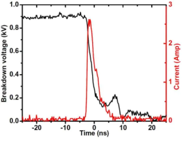
Figs. 1 and 2 demonstrate typical voltage and current waveforms from a single microplasma assisted spark gap in the pulser system [5-6]. It can also be said a single spark gap system. The details of the experimental setup are discussed in Ref. 6. The pulse rise time (10-90%) and the pulse duration at FWHM (full width half maximum) of the output current pulses at a matched load are 0.7 ns and 1.2 ns, respectively. The transferred energy for the breakdown is about 5 µJ, neglecting any losses during switching. The average power, assuming all the pulses of similar energy, at the PRR of 1.08 MHz is 5.4 watts. The total average input power for the operation of the pulser system is 18.5 watts. Since the energy involved in the switching process is very small, the operation of the spark gap has less cooling problem, thereby driving the microplasma discharges at the high PRR employing free recovery process.
Fig. 1. Breakdown voltage waveform across the spark gap at the applied voltage of 1.5 kV.
Nevertheless, some of the plasma characteristics in the
spark gap like the breakdown voltage and voltage recovery process, which are difficult to control, have some adverse effects on the output current pulses at the load. The single spark gap system requires high overvoltage to increase the PRR of the output pulses up to 1 MHz. However, the high overvoltage on the system decreases the breakdown voltage or the output current [6]. The spark gap plasma following the breakdown of the virgin gas needs definite time, through deionization and cooling of the arc channel, to reach thermodynamic equilibrium with its surrounding gas or fully recover its initial breakdown strength [7]. The duration between two current pulses or discharges decreases as the PRR increases, thereby not allowing sufficient time for the hot gas temperature T to reduce. Due to insufficient cooling of the gas temperature, the re-breakdown voltage Vbr(T) is lowered through the relation [5]
(1)
where T is the elevated gas temperature, and T0 is the initial temperature of the virgin gas.
Fig. 2. Typical voltage and current waveforms of the spark gap discharge.
Assuming Vbr(T) or simply Vbr waveform of perfectly triangular shaped (see Fig. 1) and neglecting the applied current consumed by the inductor as well as a leakage current through the spark gap in an open circuit
condition, the PRR is given by [6]
(2)
Where τ is the time between two consecutive output pulses, i0 is the applied current due to the applied voltage V0 from a high energy power supply, responsible for establishing switching of the spark gap at the high PRR, through the charging resistance RC. Here, C is the capacitance of the spark gap system when connected in the circuit assembly. Then, the system’s charging efficiency Eeff, is proportional to Vbr through the following relationship.
(3)
Since, the spark gap is integrated in a transmission line structure system, the output voltage pulse Vout at the matched load is given by [8]
(4)
The PRR increases with V0 from equation 2, while Vbr
decreases with increased V0 due to insufficient cooling at the increased PRR, thereby decreasing both Eeff and Vout.
The idea of operating several spark gaps simultaneously came up in order to achieve the high PRR without having to face aforementioned impediments. The PRR of each spark gap will be reduced to increase the cooling time for the voltage recovery so that the sum of the repetitive switching of multiple spark gaps system will be equivalent to that of the single spark gap system.
Approaches to maintain high Eeff by scaling V0 for different Vbr amplitude and the PRR have been verified experimentally. The experimental results of the two spark gaps system in this paper are mainly compared with the published results from the single spark gap system in Ref. 5 and 6.
II. Parallel Spark Gap System Fig. 3 shows the circuit diagram for the simultaneous operation of the two spark gaps in parallel. The circuit component values are typically used for the experiment.
The experimental setup is shown in Fig. 4. The length and external diameter of the spark gaps are 11.5 cm and 3.1 cm, respectively. The internal structure of the spark gaps is designed to be consistent with a 50 Ω transmission line structure, which is the commonly used coaxial cable impedance. The only discontinuity is introduced by the switch gap which is negligible due to the smallness of the gap distance. The spark gap electrodes are made of elkonite (CuW/80-20) having a diameter of 1 cm. Each of the spark gaps has two ports opposite to each other and centered at the electrode gap.
One of the ports is for the vacuum creation and insertion of SF6 gas inside the spark gap chamber. The other port is used for the gap distance measurement by a tapered feeler gauge and optical observations if required. In the present experiment, two spark gaps share a common port.
Commercially available high voltage probes (TEK:
P6015A, 75 MHz) are used for the charging voltage measurement across each of the spark gaps. The spark gaps are connected to 50 Ω loads through high bandwidth coaxial cables (RG -214) and coaxial attenuators (Lucas Weinschel, BW ~ 18 GHz). The bandwidth of the oscilloscope (TEK 3034B) is 300 MHz which is sufficient enough to measure the charging voltage waveform in the range of microseconds.
Fig. 3. Schematic circuit diagram of the pulser system.
The circuit diagram of the single spark gap system is already presented in Ref. 6. The operation of the repetitive switching in the single spark gap is carried by the charging circuit with two voltage sources. The charging resistance R1connected with the applied voltage
Fig. 4. Experimental setup for the two spark gaps system.
V1 from a high voltage power supply is 20 MΩ. R1
value remains same in the two spark gaps system as shown in Fig. 3. The charging resistance RC in both the single and two spark gaps system, connected with the applied voltage V0 from a low voltage power supply, ranges from 40 kΩ to 120 kΩ. Each of the voltage sources play distinct role for the operation of the single spark gap system. For a gas filled spark gap, the re-breakdown voltage in continuous operation is several times less than the initial breakdown voltage. Therefore, the applied voltage V1 from the high voltage supply with low energy initiates the breakdown of the virgin gas and subsequent re-breakdown becomes the function of the gas temperature. For example, the initial breakdown voltage of the spark gap with the gap distance of 300 um and the SF6 pressure of 1.25 bars is observed at about 5.1 kV. When V1 is set at this voltage, the breakdown of the spark gaps occurs occasionally and not continuous.
At a slight overvoltage of V1, the spark gap breakdown occurs continuously with the PRR in the range of a few hundreds of Hz. The applied voltage V0 from the other low voltage supply with high energy, i.e. the main power supply, is super imposed to increase the PRR of the spark gap up to 1 MHz. If the main power supply for some reasons fails to re-breakdown at the high PRR, then V1 will reignite the spark gap again. It is to be noted that the energy of the main power supply is an order of magnitude higher than the high voltage power supply. It is the reason why V1 is neglected for the
calculation of Eeff in equation (3). The two spark gaps system operate in a similar fashion as that of the single spark gap system. Therefore, they share the same voltage sources as shown in Fig. 3 but with separate charging circuit. The circuit elements in each charging circuit remain same as that of the single spark gap system.
The total capacitance of the two spark gaps system including the stray capacitance from the circuit connections is 14-17 pF. The total capacitance for the single spark gap system is 11-13 pF [5-6]. It is indeed not easy to measure the capacitance of such a low value even with a good LCR meter. However, it is important to calculate the actual Eeff of the spark gap system in real operation. Equation (3), although not includes the capacitance of the spark gap system, is a simple method to compare Eeff of the single spark gap, the two spark gaps and even multi-spark gaps system.
III. Experimental results
Fig. 5 shows the charging voltage waveform for the two spark gaps system. RC connected to each of the spark gaps in series with V0 of 1.13 kV is 110 kΩ.
Since the two spark gaps have their own charging circuit which is almost identical, their breakdown voltage waveform is nearly same. If in any case, Vbr between the two spark gaps differs, it can be stabilized by slight overvoltage of V0. There is obvious one anomaly in the voltage waveform of the two spark gaps system compared to the single spark gap system. When one spark gap discharges, a slight decrease on the charging voltage of the other spark gap is observed. This is probably due to the existence of the stray capacitance (~0.6 pF) or coupling capacitance between the two spark gaps. The repetitive Vbr of the two spark gaps takes place employing self-triggering mode without coupling each other in an independent fashion. Vbr and the PRR of each spark gap, for two different V0 values - one at 1.13 kV and the other at 1.14 kV, are shown in Fig.6.
A different V0 reading from the oscilloscope is due to measurement at different occasion. However, V0 from both the oscilloscope readings can be average out to 1.135 kV. At every V0, 3-5 readings of Vbr and the corresponding PRR for each spark gap are noted and
then average out for both the spark gaps due to similar kind of voltage waveform. The average Vbr and PRR values exceed 1 kV and 300 kHz, respectively. We are planning to increase the total PRR up to 1 MHz by operating 3-4 spark gaps in parallel in future.
In case of the single spark gap system, a certain initial V0 is necessary to start Vbr at the high PRR and then subsequent overvoltage of V0 increase the PRR to 1 MHz as desired [6]. For example, the initial V0 is 1.3 kV at which the PRR of the spark gap is 0.835 MHz using RC of 90 kΩ and the SF6 pressure of 1.25 bars.
The PRR increases to 1.59 MHz when V0 increases to 1.75 kV. Vbr at 1.3 kV and 1.75 kV is 940 V and 800 V, respectively. The initial V0 for the two spark gap
Fig. 5. Voltage waveform for the operation of two spark gaps in parallel.
Fig. 6. Typical PRR and breakdown voltage of the two spark gaps system.
systems is about 1.135 using RC of 110 kΩ and the SF6 pressure of 1.25 bars .Thus, the initial V0 is reduced for the repetitive discharge operation of the two spark gaps system compared to the single spark gap system.
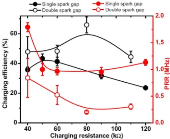
Fig. 7 compares Eeff and the PRR of the single and two spark gaps system at 1.25 bars with the gap distance of 300 µm and RC in the range of 40-120 kΩ.
Similar RC values for the two spark gaps system are used in order to increase Vbrby scaling (or reducing) V0
without overvoltage unlike that of the single spark gap system. The overvoltage is not applied for the two spark gaps system with an intension to cascade several spark gaps in parallel, thereby increasing the total PRR. The PRR of each spark gap in the two spark gaps system increases with the decrease of RC. The PRR can be increased even at higher RC by overvoltage at the cost of decreased Eeff. It is to be noted that the PRR is maintained around 1 MHz always for the single spark gap system except at 40 kΩ which is difficult to control and produces the PRR of about 1.8 MHz even without any overvoltage. Eeff is about 30-40 % for the single spark gap system whereas it exceeds 50 % for the two spark gaps system.
Fig. 7. Charging efficiency and PRR comparison of two different pulser systems.
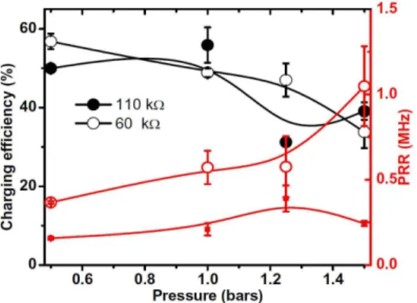
Eeff is investigated at various pressure ranges as shown in Fig. 8. Analogue pressure meter (Swagelok) has been used for this purpose with a minimum resolution of 0.25 bars starting from 1 absolute bar. Less than but close to
1 bar has been approximated to be 0.5 bars. Eeff exceeds 50 % in the range of 0.5-1.25 bars using RC of 110 kΩ.
Although not linear strictly, the PRR increases but Eeff
decreases, approximately, as the working pressure is increased. It results from the fact that V0 needed for the spark gaps to operate at the high PRR is more for higher pressure. V0 increases linearly with pressure where as Vbr remains almost the same. For example, V0
increases from 840 V at 0.5 bars to 1.2 kV at 1.5 bars using RC of 60 kΩ. V0 increases from 1 kV at 0.5 bars to 1.8 kV at 1.5 bars using RC of 110 kΩ. Similar trends were observed in the single spark gap system.
However, Vbr exceeds 1 kV in the two spark gaps system whereas it is less than 900 V for the single spark gap system.
Fig. 8. Charging efficiency and PRR for the two spark gaps system against pressure.
Either short gap distances or low pressures or low RC
or any of their combination increases the chances of dc glow as shown in Fig. 9. The movement of sparks channels at short gap distances constrained to particular position on electrode surfaces [4]. In addition, cooling is inefficient due to the decreased volume space thereby exhibiting a weak tendency to recover faster at all pressures in our experiment. Short gap distances and high gas pressure are necessary for the production of fastest rise time [1, 6]. At low gas pressure (e.g., 0.5 bars), not only the rise time degrades but also the initial ignition voltage reduces and there is a weak tendency of faster recovery at the high PRR. For example, the dc glow is observed in the electrode gap distance of 100
µm using RC up to 500 kΩ and the SF6 pressure up to 1.5 bars. Similarly, the dc glow is observed at the pressure up to 1.5 bars for the electrodes gap distance of 200 and 300 µm using RC of 40 kΩ. Also, the dc glow behavior is observed for the gap distance of 200 µm and 300 µm at the pressure up to 1.5 bars and 1 bar, respectively, using RC of 60 kΩ. The dc glow is not observed at all in the pressure range of 0.5-1.5 bars using RC of 80, 90 or 110 kΩ and the gap distance of 200 and 300 µm. The PRR is relatively small in this range (80–110 kΩ) of RC unless and until high overvoltage V0 or high i0 is applied, thereby allowing sufficient time to cooling or the voltage recovery. It is the reason why Vbr of each spark gap in the two spark gaps system is higher than the single spark gap system at the cost of reduced PRR. Overall, the experimental results from the two spark gaps system illustrate high Eeff at 1 and 1.25 bars using RC of 80 to 110 kΩ and gap distance of 200 to 300 µm. The PRR of each spark gap in all these cases are in the range of few hundreds of kHz.
Fig. 9. Typical dc glow discharges of the two spark gaps system.
IV. Conclusion
A pulser system employing a single microplasma assisted spark gap is successfully developed for the generation of fast rise time ultrashort pulses at the PRR exceeding 1 MHz. The charging efficiency at this rate of the PRR is about 30%. The pulser system is extended for the simultaneous operation of two parallel microplasma assisted spark gaps. The operation of both the spark gaps in parallel establishes similar kind of
charging and discharging waveforms in a non-synchronized fashion. The charging efficiency and PRR of each spark gap is about 50% and 300 kHz, respectively, using RC of 110 kΩ and SF6 pressure of 1.25 bars. The sum of the PRR from both the spark gaps is about 600 kHz. Thus, the successful operation of the two spark gaps pulser system demonstrates significant improvement in the charging efficiency at the cost of reduced PRR of each spark gap compared to the single spark gap pulser system. In this way, the overall PRR can be increased by cascading several spark gaps in parallel to the pulser system.
References
[1] L. Pecastaing, J. Paillol, T. Reess, A. Gibert and P.
Domens, “Design and Performance of High Voltage Pulse Generators for Ultra-Wideband Applications”, Meas.
Sci. Technol. Vol 12, pp. 1718-1725, 2001.
[2] J. M. Lehr, C. E. Baum, W. D. Prather and F. J.
Agee, “Fundamental Physical Considerations for Ultrafast Spark Gap Switching”, Ultra–Wideband, Short Pulse Electromagnetics 4, Plenum Publishers, New York, pp.
11-20, 1999.
[3] F. J. Agee, C. E. Baum, W. D. Prather, J. M. Lehr, P. O’Loughlin, Jon S. H. Schoenberg, D.W. Scholfield, R.J. Torres, J.P. Hull, J.A. Gaudet “ Ultra-Wideband Transmitter Research”, IEEE Trans. Plasma Sci. Vol 26, pp. 860-873, June 1998.
[4] H. Rahaman, B–J. Lee, I. Petzenhauser, J. Urban, R.
Stark, K. Frank, “Switching Characteristics of Micro Plasmas in a Planar Electrode Gap”, Applied Physics Letter, Vol. 90, 131505, 2007.
[5] H. Rahaman, S.H. Nam, J. W. Nam, B–J. Lee, K.
Frank, “Application of Microplasma Discharge in a Spark Gap for High Repetitive Switching”, Applied Physics Letter, Vol. 96, Issue 14, 141502, 2010.
[6] H. Rahaman, J.W Nam, S.H. Nam, K. Frank,
“Investigation of Spark Gap Discharge in a Regime of Very High Repetition Rate,” IEEE Trans. Plasma Sci., Vol. 38, No. 10, pp. 2752-2757, October 2010.
[7] S. J. Macgregor, S. M. Turnbull, F. A. Tuema, O.
Farish “Enhance Spark Gap Switch Recovery Using Nonlinear V/p Curves”, IEEE trans. Plasma Science, Vol.
23, pp 798-804, 1995.
[8] I. C. Somerville, S. J. Macgregor, O. Farish “An Efficient Stacked Blumlein HV Pulsed Generators”, Meas.
Sci. Tech. 1, pp 865-868, 1990.
BIOGRAPHY Byung-Joon Lee (member)
1998: BS degree in Physics, Kyungpook National University.
2001: MS degree in Physics, Kyungpook National University.
2000~2002: Research
Associate, Pohang Accelerator Laboratory.
2007: PhD degree in Physics, University of Erlangen-Nuremberg, Germany.
2008~2010: Habilitation (Professorship course in Germany).
2011~Present: Senior Researcher, Pohang Accelerator Laboratory.
Jong Woo Nam (Non member)
2010: Research Assistant, Pohang Accelerator
Laboratory.
2010~present: BS student in Electrical Engineering, Franklin W. Olin College of
Engineering.
Hasibur Rahaman (Non member)
1995: BSc degree in Physics, Aligarh Muslim University, India.
1997: MSc degree in Physics, Aligarh Muslim University, India.
2001: MTech degree in Microwave Engineering, Burdwan University, India
2001~2002: Research Assistant, CEERI Pilani, India
2007: PhD degree in Physics, University of Erlangen-Nuremberg, Germany.
2007~present: Researcher, Pohang Accelerator Laboratory.
Sang Hoon Nam (Non member)
1982: BS degree in Electronics Engineering, Inha University.
1984: MS degree in Physics, Hampton University.
1987: ME degree in Electrical and Computer Engineering, Old Dominion University.
1990: Ph.D degree in Electrical Engineering, University of South Carolina.
1991~2007: Chief Researcher, Pohang Accelerator Laboratory.
2007~present: Deputy Director, Pohang Accelerator Laboratory.
Jae Woon Ahn (Non Member)
1974: BS degree in Physics, Sogang University.
1984: MS degree in Physics, Hannam University.
1989: PhD degree in Physics, Chungnam University.
1976-2010: Principal Researcher, Agency for Defense Development.
2010-Present: Research Fellow, HANWHA Corporation.
Seung-Whan Jo (Non Member)
1987: BS degree in Mechanical Engineering design, Han Yang University.
1990~present: Department of Research and Development, HANWHA Corporation.
Hae-Ok Kwonn (Non Member)
1994: BS degree in Radio Science and Engineering, Korea Maritime University.
1997: MS degree in Radio Science and Engineering, Korea Maritime University.
2003~present: Department of Research and Development, HANWHA Corporation.