한국표면공학회지 J. Korean Inst. Surf. Eng.
Vol. 49, No. 5, 2016.
http://dx.doi.org/10.5695/JKISE.2016.49.5.461
<연구논문>
ISSN 1225-8024(Print) ISSN 2288-8403(Online)
비대칭 바이폴라 펄스 스퍼터법으로 증착된 VN 코팅막의 미세구조, 결정구조 및 기계적 특성에 관한 연구
전성용*, 정평근
목포대학교 신소재공학과
Microstructure, Crystal Structure and Mechanical Properties of VN Coatings Using Asymmetric Bipolar Pulsed dc Sputtering
Sung-Yong Chun*, Pyeong-Geun Jeong
Department of Advanced Materials Science and Engineering, Mokpo National University, Jeonnam 58554, Korea
(Received September 1, 2016 ; revised October 13, 2016 ; accepted October 18, 2016)
ABSTRACT
Nanocrystalline vanadium nitride (VN) coatings were deposited using asymmetric bipolar pulsed dc sput- tering to further understand the influence of the pulsed plasmas on the crystal structure, microstructure and mechanical properties. Properties of VN coatings were investigated with FE-SEM, XRD and nanoindentation.
The results show that, with the increasing pulse frequency and decreasing duty cycle, the coating morphology changed from a porous columnar to a dense structure, with finer grains. Asymmetric bipolar pulsed dc sputtered VN coatings showed higher hardness, elastic modulus and residual compressive stress than dc sputtered VN coatings. The results suggest that asymmetric bipolar pulsed dc sputtering technique is very beneficial for the reactive sputtering deposition of VN coatings.
Keywords : Pulsed Sputtering, VN, Asymmetric Bipolar, Duty cycle, Pulse frequency
1. 서 론
지난 수 년간 질화 티탄(TiN), 질화 알루미늄(AlN) 및 질화 텅스텐(WN) 과 같은 전이 금속 질화물의 산업적 응용에 대한 연구는 다수 보고되어 왔으나 높은 경도, 내마모성과 화학적 안정성에도 불구하 고 질화 바나듐(VN) 에 대한 연구는 비교적 덜 관 심을 받아왔다[1-5]. 최근 VN 코팅막은 기계 부품 공구의 표면 보호, 의료용 임플란트, 우주항공용 고 체 윤활제뿐만 아니라 리튬 이온 배터리의 전극용
신소재 등으로 산업 응용의 가능성을 확대해 나가 고 있다[6-9].현재까지 보고된 VN 코팅막의 대표 적인 제작방법으로 음극 아크(cathodic arc), dc 스 퍼터(direct current sputtering) 및 펄스 스퍼터(pulsed sputtering) 를 들 수 있다[10-12]. 특히 최근 주목 받는 방법으로 펄스 스퍼터를 들 수 있는데 이는 기존의 dc 파워 대신에 펄스 플라즈마를 생성할 수 있는 펄스 dc 전원을 사용하는 방법이다. 기존의 dc 스퍼터의 주된 문제점으로 아크 발생, 타겟 포이즈 닝(target poisoning), 불균일한 주상구조의 미세구조 생성이 보고되고 있다[13]. 본 연구실에서는 이러한 문제를 해결하기 위해 펄스 플라즈마 공정 변수를 조절할 수 있는 비대칭 바이폴라 펄스 dc 스퍼터를 이용하여 다양한 질화물 코팅막의 적용 가능성에 대해 보고한바 있다[14-16]. 펄스 dc 스퍼터를 사용
*
Corresponding Author : Sung-Yong Chun
Department of Advanced Materials Science and Engineering, Mokpo National University
Tel : +82-61-450-2495 ; Fax : +82-61-450-2498
E-mail : [email protected]
능하게 하여 코팅기술의 응용분야의 확대가 기대된 다. 최근에는 mf (mid-frequency) 및 하이브리드 mf + rf (radio frequency) 전원을 각각 이용하면 코팅막 의 미세구조 및 기계적 특성이 향상된다는 연구가 보고된 바 있으나, 본 연구와 같이 비대칭 바이폴 라 펄스 dc 스퍼터를 이용한 펄스 플라즈마 공정 변수가 VN 코팅막의 물성에 미치는 영향에 대해 조사한 연구는 보고된 바 없다[17].
따라서 본 연구에서는 우수한 기계적 물성을 얻 을 수 있는 비대칭 바이폴라 펄스 플라즈마가 VN 코팅막의 미세구조적, 물리 결정화학적 및 기계적 특성에 미치는 영향에 대해 연구하였다. 특히 비대 칭 바이폴라 펄스 dc 스퍼터로 VN 코팅막을 제작 할 때 듀티 싸이클과 펄스 주파수와 같은 펄스 플 라즈마 공정 변수가 코팅막의 표면 및 단면 미세구 조, 결정구조, 우선배향성, 잔류응력 및 기계적 특 성 등에 미치는 영향에 대해 주목하였다.
2. 실험방법
본 실험에서는 펄스 플라즈마 공정 변수를 조절 할 수 있는 비대칭 바이폴라 펄스 dc 스퍼터를 사 용하여 표 1 처럼 모두 4가지 종류의 VN 코팅막 을 제작하였다. 출발원료로는 직경 3'', 두께 1/4'', 순도 99.9 %의 V 타겟과 초고순도의 Ar과 N2 가스 를 사용하였다. Ar과 N2주입량은 각각 31 sccm 과 5 sccm으로 고정하였고 증착 시 기판과 타겟간 거 리는 60 mm로 유지하고, 균일한 코팅을 위해 기판 을 약 10 rpm의 속도로 회전시켰다. Si(100) 기판 표면의 불순물을 제거하기 위하여 초음파 세척기를 이용하여 아세톤과 에틸 알코올에서 각각 10분간 세척을 실시한 후 건조하였다. 챔버의 초기압력은 로터리 펌프와 터보분자 펌프를 사용하여 약 1.4 × 10⁻³ Pa까지 배기시켰으며 총 공정압력 (Ar+N2) 은
팅막의 결정구조, 우선 배향성 및 잔류응력 등의 분 석을 위해 고분해능 XRD (PAN analytical사 / X’pert- pro MRD) 를 사용하였고, FE-SEM (Hitachi사/
S-3500N) 을 이용하여 코팅막의 표면과 단면의 미 세구조를 관찰하였다. 경도는 Berkovich 다이아몬 드 압자를 이용하여 16번의 실험을 통한 평균값으 로 구하였다. 나노인덴터 측정 간격은 이미 실행된 경도 측정 팁에 영향을 받지 않기 위해 10 μm 이 상을 유지 하였다.
3. 결과 및 고찰
본 연구에서는 비대칭 바이폴라 펄스 dc 스퍼터 를 이용하여 공정변수를 변화시켜 4가지 종류의 코 팅막을 제작하였고 VN 코팅막의 표면 및 단면 미 세구조, 결정구조, 우선배향성, 잔류응력 및 기계적 특성에 미치는 영향에 대해 조사하였다.
3.1. 미세구조
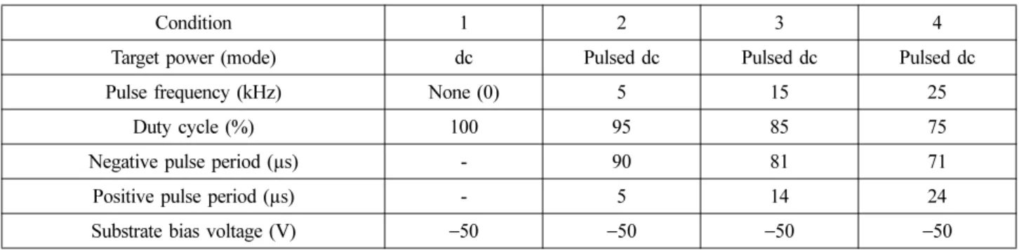
비대칭 바이폴라 펄스 dc 스퍼터로 제작된 VN 코팅막의 미세구조를 FE-SEM을 이용하여 관찰하 였고 그 표면과 단면사진을 그림 1에 나타내었다.
Condition 1 (dc 모드) 에서 제작된 코팅막의 표면 사진에서는 condition 4 (pulsed dc 모드)에서 얻어 진 코팅막에 비해 거친 쐐기 (facet) 형상의 다면체 입자들이 관찰되었으나 condition 4 에서 제작된 코 팅막의 표면 사진에서는 매끄럽고 입계를 구분하기 어려울 정도로 미세화된 둥근 (round) 형상의 입자 들을 관찰 할 수 있다. 한편 condition 1 에서 제작 된 코팅막의 단면 사진에서는 표면에서 관찰된 쐐 기형상의 다면체 입자로부터 연장된 주상구조 입자 와 함께 주상구조의 입자들 사이로 주상형 기공 (inter-columnar voids)이 다수 관찰되었다. 한편 condition 4 에서 제작된 코팅막의 단면 사진에서는
Table 1. Conditions for deposition of VN coatings using asymmetric bipolar pulsed dc sputtering
Condition 1 2 3 4
Target power (mode) dc Pulsed dc Pulsed dc Pulsed dc
Pulse frequency (kHz) None (0) 5 15 25
Duty cycle (%) 100 95 85 75
Negative pulse period (µs) - 90 81 71
Positive pulse period (µs) - 5 14 24
Substrate bias voltage (V) −50 −50 −50 −50
다공성 주상구조가 사라지고 코팅막 표면으로부터 기판과 코팅막의 계면까지 매우 치밀한 미세구조가 관찰되었다.
본 연구에서 사용한 비대칭 바이폴라 펄스 dc 스 퍼터는 기존의 dc 스퍼터에 비해 높은 이온화율과 고 밀도 플라즈마를 얻을 수 있다. 따라서 이러한 높은 이온화율과 고밀도 플라즈마는 기판으로 입사 하는 하전입자의 운동에너지의 증가에 영향을 미치 고 기판 표면에서의 이동도 향상 및 핵생성 밀도를 증가시켜 치밀한 미세구조의 코팅막의 제작이 가능 하게 되었다고 사료된다. 또한 코팅 중 dc –50 V 의 기판 바이어스 전압을 인가했기 때문에 수 십 eV 범위의 이온 에너지 분포를 갖는 다수의 하전 입자들에 의한 이온 포격 효과도 핵생성 밀도 증가 에 기여했다고 사료된다[18].
3.2. 결정구조 및 우선 배향성
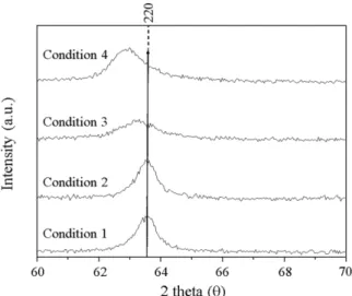
비대칭 바이폴라 펄스 dc 스퍼터로 제작한 VN 코팅막의 X선 회절분석 결과를 그림 2에 나타내었 다. 모든 코팅 조건에서 단일상의 입방정계 면심입 방구조 (cubic fcc)의 VN 코팅막이 생성되었으며 모 두 (111)면, (200)면, (220)면, (311)면의 피크가 관 찰되었다 (JCPDS 25-1252). 한편 VN 코팅막의 우 선 배향성은 펄스 플라즈마 공정변수에 따라 다음 과 같이 변화함을 알 수 있다. 즉 Condition 1 에서 는 (111)면, condition 3 에서는 (200)면, 그리고 condition 4 에서는 (220)면에서 높은 상대강도의 X 선 피크가 관찰되었다. 즉 펄스 플라즈마 코팅 조 건에 따라 VN 코팅막의 우선배향성은 (111)면, (200)면, (220)면 순으로 변화하였다. 일반적으로 코 팅막의 결정상 및 우선배향성의 변화에 영향을 미
치는 공정변수로 Ar/N2의 혼합비, 기판바이어스 전 압 등은 다수 보고된 바 있으나, 이렇듯 펄스 플라 즈마 공정변수가 코팅막의 우선 배향성에 영향을 미칠 수 있다는 연구결과는 거의 보고된 바 없다 [19-21].
3.3. 잔류응력
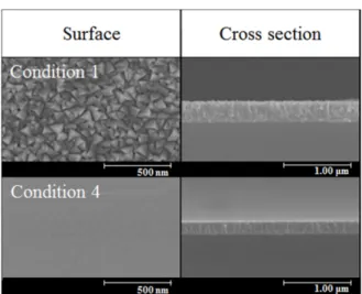
비대칭 바이폴라 펄스 플라즈마 공정변수가 VN 코팅막의 잔류응력에 미치는 영향을 보다 자세히 알아보기 위해 (220)면의 X선 피크의 2θ 값의 변 화를 표 2와 그림 3에 각각 나타내었다. 얻어진 VN 코팅막의 회절 피크의 포지션 변화에 미치는 영향 을 쉽게 이해하기 위해 JCPDS 카드 (#25-1252)로 부터 구한 표준 2θ값도 함께 표시하였다. (220)면 의 경우 피크의 2θ 값은 condition 1 에서 63.50o, condition 3 에서 63.30o, condition 4 에서 62.98o로 JCPDS 카드 표준 값 64.35o보다 작음을 알 수 있 다. 특히 코팅조건 condition 1부터 condition 3, condition 4의 순으로 VN 코팅막의 (220)면의 X선 피크의 2θ 값은 낮은 저각으로 이동함을 알 수 있 다. 이러한 2θ 값의 저각으로의 이동은 주로 잔류 응력의 내부 압축응력의 증가에 기인한다고 보고되 고 있다[22,23]. 일반적으로 PVD (Physical Vapor Deposition)를 이용하여 제작된 코팅막에는 잔류응
Fig. 1. Top surface and cross-sectional FE-SEM
images of VN coatings using asymmetric bipolar pulsed dc sputtering.
Fig. 2. XRD data of VN coatings using asymmetric bipolar pulsed dc sputtering.
Table 2. XRD data of VN coatings using asymmetric bipolar pulsed dc sputtering
VN Peak position
(220)
Condition 1 2 3 4 standard
2θ (
o) 63.50 63.50 63.30 62.98 64.35
사료된다[24].
3.4. 나노 경도 및 탄성률
비대칭 바이폴라 펄스 dc 스퍼터법으로 제작한 VN 코팅막의 경도와 탄성률을 측정하기 위해 나노 인덴테이션 장비를 이용하였다. 측정결과의 신뢰도 향상을 위해 샘플당 1 마이크로미터 단위로 30 개 소 이상의 장소에서 측정하여 얻어진 평균 경도와 탄성률 결과를 그림 4에 나타내었다. 수십 ~ 수백 nm의 두께를 갖는 얇은 코팅막의 경도측정은 기존 의 마이크로 비커스 경도계로는 측정이 거의 불가 능하고 인덴테이션 크기 효과로 인해 정밀한 측정 이 매우 어렵다[25]. 이와 달리 본 연구에 사용되 는 나노인덴테이션 기술은 아주 작은 양의 재료의 기계적 성질을 얻기 위해 가장 간단하고 직접적인
이 증가하는 경향을 보이는 인덴테이션 크기 효과 를 배제하기 위하여 전체 막 두께의 1/10 지점으로 평균화하였다[27].
그림 4에서 코팅막의 나노인덴테이션 경도와 탄 성률은 비대칭 바이폴라 펄스 플라즈마 코팅조건에 따라 거의 연속적으로 증가함을 확인 할 수 있다.
condition 4에서 제작된 VN 코팅막의 나노인덴테이 션 경도와 탄성률은 각각 약 15.9 GPa과 186.4 GPa 로 condition 1에서 제작된 코팅막의 약 11.9 GPa 와 155.5 GPa에 비해 경도는 약 33%, 탄성률은 20%
까지 각각 증가함을 알 수 있다. 이러한 VN 코팅 막의 나노 경도와 탄성률의 상승원인으로 펄스 플 라즈마 생성에 따른 하전 입자들의 고이온화와 기 판바이어스 전압인가에 따른 높은 Ar+ 이온포격효 과, 중성 원자 및 분자의 지속적인 충돌로 인한 코 팅막의 결정립 미세화와 압축응력의 상승 등과 같 은 복합적인 요소에 기인한다고 사료된다.
4. 결 론
본 연구에서는 비대칭 바이폴라 펄스 dc 스퍼터 장비를 이용하여 펄스 플라즈마 공정변수를 변화시 켜 4가지 종류의 단일상의 입방정계 면심 입방구조 를 갖는 나노결정질 VN 코팅막을 제작하였다.
Condition 1에서 제작된 코팅막의 표면에서는 거친 쐐기형상의 다면체 입자들이 단면에서는 주상구조 의 입자들 사이로 주상형 기공 미세구조가 관찰되 었으나 condition 4 에서 제작된 코팅막의 표면에서 는 매끄럽고 미세한 둥근 입자가 단면에서는 주상 구조가 사라진 치밀한 미세구조가 관찰되었다. 모 든 코팅조건에서 단일상의 VN 코팅막이 얻어졌으 나 우선배향성은 condition 1에서 (111)면, condition 3에서 (200)면, condition 4에서 (220)면 순으로 변 화하였다. 또한 VN 코팅막의 (220)면 X선 피크의 2θ 값은 코팅조건에 따라 표준샘플의 2θ 값 보다 낮은 저각으로 이동하였으며 이로부터 잔류응력의 내부 압축응력이 증가함을 알 수 있었다. VN 코팅 막의 나노인덴테이션 경도와 탄성률은 condition 4 에서 각각 약 15.9 GPa과 186.4 GPa로 condition 1 에서 제작된 코팅막의 약 11.9 GPa와 155.5 GPa 에 비해 경도는 약 33%, 탄성률은 20% 까지 각각 증가하였다.
Fig. 3. XRD patterns of maximum peak (220) with shift toward low angles in relationship to the increasing of applied DC Pulsed.
Fig. 4. The nanoindentation hardness and Elastic
Modulus of VN coatings using asymmetric bipolar
pulsed dc sputtering.
감사의 글
본 과제(결과물)는 산업통상자원부의 출연금으로 수행한 전남대불산학융합지구조성 사업의 연구결과 입니다.
References