Vol. 21, No. 5 (2011)
268
†Corresponding author
E-Mail : [email protected] (D. Kim)
Growth and Characterization of GaN on Sapphire and Porous SWCNT Using Single Molecular Precursor
P. V. Chandra Sekar, Hyunchul Lim, Chang Gyoun Kim* and Dojin Kim
†Department of Materials Science and Engineering, Chungnam National University, Daejeon 305-764, Korea
*Korea Research Institute of Chemical Technology, Daejeon 305-600, Korea
(Received March 18, 2011 : Received in revised form April 11, 2011 : Accepted April 13, 2011)
Abstract
Due to their novel properties, GaN based semiconductors and their nanostructures are promising components in a wide range of nanoscale device applications. In this work, the gallium nitride is deposited on c-axis oriented sapphire and porous SWCNT substrates by molecular beam epitaxy using a novel single source precursor of Me2Ga(N3)NH2C(CH3)3 with ammonia as an additional source of nitrogen. The advantage of using a single molecular precursor is possible deposition at low substrate temperature with good crystal quality. The deposition is carried out in a substrate temperature range of 600-750oC. The microstructural, structural, and optical properties of the samples were analyzed by scanning electron microscopy, X-ray diffraction, Raman spectroscopy, and photoluminescence. The results show that substrate oriented columnar-like morphology is obtained on the sapphire substrate while sword-like GaN nanorods are obtained on porous SWCNT substrates with rough facets. The crystallinity and surface morphology of the deposited GaN were influenced significantly by deposition temperature and the nature of the substrate used. The growth mechanism of GaN on sapphire as well as porous SWCNT substrates is discussed briefly.Key words
gallium nitride, porous SWCNT, single source precursor.1. Introduction
Because of its wide band gap (3.4 eV) and high exciton binding energy, gallium nitride (GaN) has attracted much attention in the past years, notably for optoelectronic applications such as blue and green LEDs and lasing devices operating at room temperature, detectors, sensors and field emitters.
1-4)Currently, device quality epitaxial GaN deposition is being carried out by metal-organic chemical vapor deposition (MOCVD), molecular beam epitaxy (MBE), hydride vapour phase epitaxy (HVPE), etc. In all these methods high temperature processing is the inevitable problem leading to limited substrate choice. In recent years, the low temperature synthesis of poly- crystalline GaN and amorphous GaN has also attracted towards optoelectronic device application.
5,6)One of the alternative to deposit GaN at low temperature is to employ single source molecular precursor.
7)In principle, single molecular precursors provide the unique advantage of preformed Ga-N bonding and controlled composition of the resulting product. Thus single molecular precursors have been investigated as an alternative source for the nitride semiconductors.
8,9)For the growth of epi-layers, however, single molecular precursors seem to be of
limitation in view of optical and structural quality due to low temperature growth.
The purpose of this article is to study the growth mechanism of single source precursor GaN on sapphire under ammonia atmosphere. Here we demonstrated the growth of GaN thin films on sapphire and its extension to growth on porous SWCNT substrates. The substrate morphology has significant effect on the nature of growth mechanism.
2. Experimental Procedure
The unique source for the GaN growth was a single molecular GaN precursor source of Me
2Ga(N
3)(NH
2t-Bu).
The preparation of single precursor source was explained
in our previous report.
10)GaN layers were grown on
sapphire (0001) at a substrate temperature (T
s) of 600
oC to
750
oC using MBE. The substrates were degreased and etch
cleaned by conventional method before loading into the
MBE chamber. The background pressure of MBE was low
at ~10
–9torr with liquid nitrogen flow. The GaN molecular
precursor of white powder was heated to ~63
oC and the
flux was varied in the range of 10
–7- 10
–6torr using a
micro-valve to control the deposition rate. Ammonia with
purity of 99.99% was used in addition to single source
precursor flux. The ammonia flow rate is controlled in the
range of 4-20 sccm. The porous SWCNT substrates used
in our study is synthesized by modified arc-discharge method. The detailed procedure for the synthesis of porous SWCNT templates has been reported previously.
11)Thickness of the as grown thin films was measured by an alpha step profiler. The surface morphology of the grown samples was analyzed by field emission scanning electron microscopy equipped with EDS (FESEM: JEOL 7000). The structural properties were examined by X-ray diffraction technique using Rigaku 12KV XRD using Cu K α (λ = 1.5406 Å) radiation. Raman spectra were taken at room temperature using 514.5 nm incident photons from an Ar ion laser (JY LabRam HR) in a backscattering geometry. Photoluminescence measurement was also per- formed at 4K with a 325 nm line of a He-Cd laser as an exciton source to analyze the optical behavior of the samples.
3. Results and Discussion
The GaN thin film samples discussed in this article have been deposited at a fixed working pressure of 4 × 10
−6torr and substrate temperatures in the range of 600-750
oC. Fig.
1 shows graphical representation of growth rate evolution of GaN thin films as a function of growth temperature on sapphire substrate. The growth rates of GaN thin films have been measured by alpha step profiler and SEM. Two distinct growth temperature regions were observed. This distinct feature in growth mechanism is observed in CVD growth of GaN, SiC, ZnO thin films.
12-14)The lower tem- perature region is governed by kinetically controlled deposition in which the surface decomposition of the precursor with ammonia is the rate determining step. The activation energy for the GaN film deposition calculated experimentally from the slope of Fig. 1b is approximately 46.5 KJ/mol. In the temperature region of above 650
oC, however, the Arrhenius plot shows a positive slope with negative activation energy of ( −37.2 KJ/mol), indicating that the growth rate is controlled by the mass transport of reagents through the boundary layer to the growth surface.
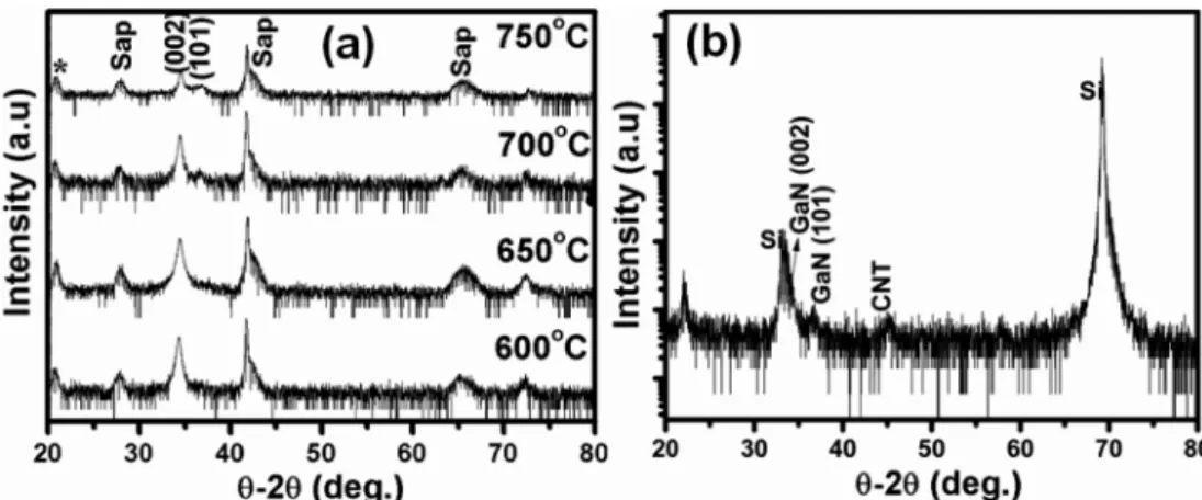
13)Fig. 2(a) shows the θ-2θ XRD patterns for the GaN films grown on sapphire substrate as a function of deposition temperature. Note that we have used the logarithm of the intensities in order to be able to identify even small
Fig. 1. (a) GaN thin film growth rate as a function of substrate temperature and (b) its Arrhenius plot.
Fig. 2. (a) X-ray diffraction pattern of GaN thin films deposited on sapphire at different substrate temperatures and (b) GaN deposited on porous SWCNT at substrate temperature of 650oC.
features. The crystallinity of the film strongly depends on substrate temperature. XRD peaks (0002), (0004) related to wurtzite structure of GaN (JCPDS file ID 500792) only appeared at substrate temperature of 600
oC and 650
oC.
Absence of peaks other than (0002) and (0004) confirms that a highly substrate oriented growth was resulted. Above 650
oC, a weak XRD peak at 36.52
oattributed to (10 1) of wurtzitic GaN begins to appear and becomes stronger at higher temperature. It should be noted that no low- temperature buffer layer is employed in our experiment.
By adopting the condition for the highest growth rate at 650
oC, deposition of GaN is carried out on porous SWCNT substrates. The XRD pattern of GaN deposited on porous SWCNT substrates at T
s= 650
oC is presented in
Fig. 2(b). Only the GaN (002) and (101) peaks were found in the spectrum. A peak originated at 44.9
ocorresponds to graphitic CNT.
Fig. 3(a)-3(d) shows a representative FE-SEM image and the corresponding cross-section image (inset) of GaN thin films grown at different substrate temperatures. At 600
oC and 650
oC morphology of relatively smooth surface with small grains was observed. Above 650
oC grain size increased abruptly to form crystallites with grain boundary leading to a rough surface. The rough surface morphology implies that a complete decomposition of single source precursor leaves gallium metal droplets which react with ammonia to form GaN crystallites. It was reported that decomposition of single source molecular precursor at high
1Fig. 3. FESEM images of GaN thin films grown at (a) 600oC, (b) 650oC, (c) 700oC and (d) 750oC. (e) Low magnification image of GaN nanorods grown on SWCNTs at 650oC and (f) highly magnified image of (e).
temperatures leads to gallium rich GaN.
15)It is to be noted that columnar like morphology is clearly evident from the cross sectional image. The columnar like grains are grown normal to the substrate surface which is also confirmed from the X-ray diffraction pattern. Fig. 3(e) and 3(f) depict the morphology of GaN deposited on porous CNT sub- strates. It is clearly shown that most of the nanorods are grown along the nanotube rather than on the substrate.
From high resolution image shown in Fig. 3(f) verified that as grown nanorods possess sharp tip with rough surface.
We conclude that growth of nanorods might be due to nature of the substrate as will be discussed elsewhere.
16)Fig. 4 shows Raman spectra of GaN films grown on sapphire substrate at various temperatures. In general, for GaN films grown along c-axis, E
2and A
1(LO) modes are observed normally due to their symmetry selection rule for the wurtzite crystal.
17)It can be seen from the figure that
asymmetric broad band is observed between 435-835 cm
−1which shows highly disordered structure. The characteristic E
2phonon mode is not clearly observed in our samples.
However, A
1(LO) is clearly seen at 715 cm
−1and the peak shifting towards higher frequency range indicates enhanced crystalline quality (568 and 734 cm
−1for E
2and A
1of bulk crystals). For samples grown at 750
oC, A
1(LO) of 735 cm
−1is obtained which is close to the bulk value.
A broad Raman peak centered at 1373 cm
−1is observed in samples grown at 600
oC. This broad peak split into two peaks centered at 1347 cm
−1and 1597 cm
−1for the growth above 650
oC. These two peaks are without doubt related to carbon impurities supplied by single source material containing carbon. These two peaks are also commonly observed in carbon nanotube as D- and G-band corres- ponding to defects on the wall of CNTs and the graphitic layer of CNTs, respectively. Sun et al.
18)reported that the
Fig. 4. Raman Spectra of GaN thin films grown on (a) sapphire substrate and (b) porous SWCNT substrate at 650oC.
Fig. 5. Photoluminescence spectra of GaN thinfims grown on (a) sapphire substrate and (b) porous SWCNT substrate at 650oC.
GaN samples implanted with carbon and post-annealed showed sharp peaks at 1350 and 1600 cm
−1due to forma- tion microcrystalline graphitic layer which could be dis- appeared above 1100
oC. So we conclude that the origin of carbon impurity is the carbon containing organometallic precursor which could not be removed even at high tem- perature growth process. At the deposition temperature of 650
oC and above, carbon impurities are diffused into the grain boundaries and crystallized into graphite. Fig. 4(b) compares the Raman spectra of porous SWCNTs and GaN/
SWCNTs. A very strong peak at 1596 cm
−1(G-band) is related to the tangential vibration of carbon atoms and that at 1354 cm
−1(D-band) is related to disordered sp
3hybridized carbon as impurities and defects. The observation of an increased intensity of D-band suggests a breakage of the graphitic crystallinity upon deposition of GaN.
Fig. 5(a) presents the PL spectrum of the samples deposited at substrate temperature of 600-750
oC. The spectra consist of an in homogenously broadened band in the range of 360 nm to 640 nm with a maximum in the blue-green at 508 nm (2.44 eV). The broad luminescence spectra might be due to low temperature processing temperature. Reynolds et al.
19)have discussed a source of the yellow luminescence in GaN and shown that its origin is best explained by a transition between a shallow donor and a deep level. The impurities such as carbon and oxygen were also the source of broad yellow luminescence. The substrate temperature does not influence the luminescence behavior significantly as observed. In case of GaN nanorod on SWCNTs, sharp luminescence peak is observed as shown in Fig. 5(b). This observation indicates that reduction of defect density in GaN nanostrucutres compared with GaN thin films.
4. Conclusion
We demonstrated that the concept of single molecular precursor could be useful for hybridization of GaN nanorods with SWCNTs at low temperatures. The surface morphology analysis by FE-SEM revealed that the as- deposited thin films grown on sapphire show a substrate oriented growth (columnar growth) until 650
oC while above 650
oC, disordered GaN crystal domains are formed with well separated grain boundaries. On the contrary, sword-like GaN nanorods structures were obtained on porous SWCNT substrates. The growth rate and Arrhenius plot presents the deposition kinetics of GaN thin films.
Acknowledgement
This study was supported by research fund of Chungnam National University, Korea.
References
1. S. Nakamura, Y. Harada and M. Senoh, Appl. Phys. Lett., 58, 2021 (1991).
2. S. J. Pearton, C. B. Vartuli, J. C. Zolper, C. Yuan and R.
A. Stall, Appl. Phys. Lett., 67, 1435 (1995).
3. F. A. Ponce and D. P. Bour, Nature, 386, 351 (1997).
4. S. Nakamura and G. Fasol, The blue laser diode : GaN based light emitters and lasers, p.201-205, Springer, Berlin (1997).
5. D. P. Bour, N. M. Nickel, C. G. Van de Walle, M. S.
Kneissl, B. S. Krusor, P. Mei and N. M. Johnson, Appl.
Phys. Lett., 76, 2182 (2000).
6. A. Koo, F. Budde, B. J. Ruck, H. J. Trodahl, A. Bittar, A.
Preston and A. Zeinert, J. Appl. Phys., 99, 034312 (2006).
7. M. M. Sung, C. G. Kim and Y. S. Kim, J. Vac. Sci. Tech., 22, 461 (2004).
8. A. Y. Timoshkin, H. F. Bettinger and H. F. Schaefer, J.
Cryst. Growth, 222, 170 (2001).
9. D. M. Hoffmann, S. P. Rangarajan, S. D. Athavale, D. J.
Economou, J. R. Liu, Z. Zheng and W. K. Chu, J. Vac.
Sci. Tech., 14, 306 (1996).
10. K. H. Kim, K. J. Lee, H. S. Kang, F. C. Yu, J. A. Kim, D. J. Kim, K. H. Baik, S. H. Yoo, C. G. Kim, Y. S. Kim, C. S. Kim, H. J. Kim and Y. E. Ihm, Phys. Status Solidi B, 241, 1458 (2004).
11. N. D. Hoa, N. V. Quy, Y. Cho and D. Kim, Sensor.
Actuator. B Chem., 135, 656 (2009).
12. A. Devi, W. Rogge, A. Wohlfart, F. Hipler, H. W. Becker and R. A. Fischer, Chemical Vapor Deposition, 6, 245 (2000).
13. J. H. Boo, S. B. Lee, K. S. Yu, M. M. Sung and Y. Kim, Surf. Coating. Tech., 131, 147 (2000).
14. J. Zhu, R. Yao, H. Song, Z. Fu, A. Yu. Kuznetsov and I.
H. Lee, J. Vac. Sci. Tech., 26, 224 (2008).
15. S. A. Rushworth, J. R. Brown, D. J. Houlton, A. C. Jones, V. Roberts, J. S. Roberts and G. W. Critchlow, Adv. Mater.
Optic. Electron., 6, 119 (1996).
16. H. C. Lim, P. V. Chandrasekar, D. M. Chang, S. Y. Ahn, H. Jung and D. Kim, Kor. J. Mater. Res., 20, 199 (2010) (in Korean).
17. H. Harima, J. Phys. Condens. Matter., 14, R967 (2002).
18. W. H. Sun, S. T. Wang, J. C. Zhang, K. M. Chen, G. G.
Qin, Y. Z. Tong, Z. J. Yang, G. Y. Zhang, Y. M. Pu, Q.
L. Zhang, J. Li, J. Y. Lin and H. X. Jiang, J. Appl. Phys., 88, 5662 (2000).
19. D. C. Reynolds, D. C. Look, B. Jogai, J. E. Van Nostrand, R. Jones and J. Jenny, Solid State Comm., 106, 701 (1998).