1. 서 론
DLC (diamond-like carbon) 박막은 우수한 경도, 낮은 마찰 계수, 화학적 안정성, 높은 내마모성, 적외선 영역에서의 높은 투과율 등의 많은 장점을 가진다. 지금 까지 DLC 박막은 마그네틱 미디어와 하드디스크의 슬라 이딩 표면, MEMS 소자와 MMAs (moving mechanical assemblies)의 고체 윤활 코팅 등으로 사용되고 있으
a. Corresponding author; [email protected] Copyright ©2018 KIEEME. All rights reserved.
This is an Open-Access article distributed under the terms of the Creative Commons Attribution Non-Commercial License (http://creativecommons.org/licenses/by-nc/3.0) which permits unrestricted non-commercial use, distribution, and reproduction in any medium, provided the original work is properly cited.
며, 최근 생체적합 물질로써 의공학 관련 부품소재로써 다양하게 응용되고 있다 [1-5]. 그러나 의공학 응용을 위한 낮은 접착력과 높은 잔류응력은 개선하기 위한 노력이 필요하다. DLC 박막의 이러한 단점을 개선하 기 위해 DLC 박막 내에 금속(Metal)이나 실리콘(Si)을 첨가하거나 중간층을 삽입하여 접착력과 잔류응력을 해결하기 위한 노력들이 진행되고 있다 [1-5]. 특히 금 속 질화물/금속 탄화물 등은 낮은 전기저항, 장기간 좋은 부식특성 및 화학적 안성성 등 우수한 전기적⋅
물리적 특성을 바탕으로 확산 방지층뿐만 아니라 다양 한 반도체 소자인 태양전지 접촉층, 전계효과 트랜지스 터의 접촉전극으로 응용되고 있다.
따라서 본 연구에서는 탄소 박막의 접착력을 향상시
생체 적합 소재 응용을 위한 비대칭 마그네트론 스퍼터링으로 제작된 Ni 도핑된 탄소 박막의 제조 및 특성
김광택1, 박용섭2,a
1 호남대학교 전자공학과
2 조선이공대학교 전자과
Fabrication and Characteristics of Ni Doped Carbon Thin Films Prepared by Unbalanced Magnetron Sputtering for the Application of Biomaterials
Kwang-Taek Kim
1and Yong Seob Park
2,a1 Department of Electronic Engineering, Honam University, Gwangju 62399, Korea
2 Department of Electronics, Chosun College of Science and Technology, Gwangju 61453, Korea
(Received November 12, 2017; Revised December 7, 2017; Accepted December 12, 2017)
Abstract: Various Ni-doped carbon (C:Ni) thin films were fabricated using different Ni target power densities by unbalanced magnetron sputtering (UBM). The effects of target power density on the structural, physical, surface, and electrical properties of C:Ni films were investigated. The UBM C:Ni thin films exhibited uniformly smooth surfaces.
The rms surface roughness and friction coefficient values of the C:Ni films decreased with the increase in target power density. The physical properties of the films such as hardness and elastic moduli increased while their electrical properties such as resistivity decreased with the increase in the target power density. These results show that an increase of the power density leads to an increase in the proportion of Ni and nanocrystallization of the amorphous carbon film;
this contributes to the changes observed in the physical and electrical characteristics.
Keywords: Ni doped carbon film, Unbalanced magnetron sputtering, Hardness, Friction coefficient, Resistivity
Regular Paper 40
J. Korean Inst. Electr. Electron. Mater. Eng.
Vol. 31, No. 1, pp. 40-43 January 2018 DOI: https://doi.org/10.4313/JKEM.2018.31.1.40 ISSN 1226-7945(Print), 2288-3258(Online)
전기전자재료학회논문지, 제31권 제1호 pp. 40-43, 2018년 1월: 김광택 등 41
키고 잔류응력을 줄이기 위해 탄소 박막 내 Ni 금속을 도핑하고자 비대칭 마그네트론 스퍼터링 시스템을 이 용하여 Ni 타겟 전력 밀도에 따라 제작된 C:Ni 박막 의 구조적⋅물리적, 트라이볼로지 특성들을 평가하고 고찰하였다.
2. 실험 방법
니켈(Ni) 도핑 탄소박막(C:Ni)은 4인치인 Ni 타겟과 흑연(graphite) 타겟을 부착한 비대칭 마그네트론 스퍼 터링(unbalanced magnetron sputtering) 시스템을 이용하여 증착하였다. 2.5×2.5 cm2 크기의 실리콘 기 판을 사용하고, 박막 증착전 챔버의 초기 진공도는 1×10⁻⁵ Torr로 유지하고, 스퍼터링을 위해 99.99%의 아르곤(Ar)을 가스를 주입하여 증착 압력을 2×10⁻³ Torr로 설정하였다. 기판은 20 rpm으로 회전시켰으 며, 타겟과 기판 사이의 거리는 60 mm로 하고 흑연 타겟의 전력 밀도는 25 W/cm2로 고정하였다. 탄소 박막에 Ni 도핑량은 Ni 스퍼터 타겟의 전력 밀도를 2~5 W/cm2로 조절하여 변화시켰다. 박막의 두께는 100 nm로 증착하였으며, 제작된 박막의 구조적⋅물리 적, 트라이볼로지 특성들은 field emission scanning electron microscope (FESEM: XL-40aFEG), atomic force microscope (AFM, NITECH, SPM 400), X-ray photoelectron spectroscopy [XPS-PHI5200] (Al Kα radiation source in an ultra high vacuum), 나노인 덴터, 나노스크레치테스터, 접촉각(contact angle) 등 4-point probe로 측정하여 값을 도출하였고, 연구 결과 를 고찰하였다.
3. 결과 및 고찰
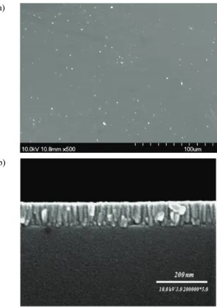
그림 1은 Ni 타겟 전력 밀도에 따라 제작된 C:Ni 박막의 FESEM 분석에 의해 측정된 표면과 단면의 모 습을 나타낸다. 표면 그림에서 확인할 수 있듯이, Ni 타겟 전력 밀도에 따라 제작된 박막 표면은 균일하고 결함이 없는 것을 확인할 수 있다.
또한 단면에서 보듯이, 수직 방향으로 성장되었음을 확인하였다. 이러한 결과는 탄소박막이 형성되는 동안 seed 역할로써 Ni 금속이 영향을 미쳤을 것이라고 판 단된다.
그림 2는 Ni 타겟 전력 밀도에 따라 증착된 C:Ni
박막의 증착률과 탄소 박막 내에 포함된 Ni 원자 구성 비율을 나타낸다. 결과에서 보듯이, Ni 타겟 전력 밀도 가 증가함에 따라 박막 내 포함된 Ni 원자의 비율은 Fig. 2. Growth rate of C:Ni thin film and Ni concentration contained in C:Ni films with the increase of Ni target power density.
(a)
(b)
Fig. 1. FESEM surface and cross-sectional images of C:Ni thin films deposited at the conditions of 5 W/cm2 Ni target power density.
J. Korean Inst. Electr. Electron. Mater. Eng., Vol. 31, No. 1, pp. 40-43, January 2018: K.-T. Kim et al.
42
증가되었다. 이러한 결과는 Ni 타겟 전력 밀도의 증가 에 따라 Ni 타겟으로부터 스퍼터링 된 Ni 원자의 비율 이 증가되어 기판 표면에 도달되는 Ni 원자 비율이 증 가되었기 때문이다 [6-8].
그림 3은 Ni 타겟 전력 밀도에 따라 제작된 C:Ni 박막의 Rms 표면 거칠기 값과 마찰계수 값의 변화를 보여준다. 결과에서 보듯이, C:Ni 박막 표면에서의 Rms 표면 거칠기 값과 마찰계수 값은 Ni 타겟 전력 밀도 증가에 따라 감소하였다. 결과에서 표면 거칠기 값의 감소이유는 스퍼터링 된 탄소와 Ni 금속 원자들 의 증가에 의한 충돌 횟수의 증가 때문이며, 또한 결 합에 참여하는 금속과 탄소원자가 결합에 의해 비정질 구조에서 나노 크기의 결정화로 변화되는 과정에서 일 어나는 현상이라고 판단된다. 결론적으로 이러한 결과
는 Ni 타겟 전력 밀도 증가에 의한 금속원자 함유량의 증가는 나노 크기의 결정성을 향상시키는 원인이 되며, 스퍼터링 증가를 야기해 기판 표면 온도 향상에 기여 하기 때문이라고 판단된다 [6,9,10].
그림 4는 Ni 타겟 전력 밀도에 따라 증착된 C:Ni 박막의 경도와 탄성계수 값의 변화를 나타낸다. 결과에 서 보듯이 C:Ni 박막의 경도와 탄성계수 값은 Ni 타 겟 전력 밀도 증가에 따라 증가하였고, Ni 타겟 전력 밀도 4 W/cm2에서 최댓값은 각각 26.5 GPa과 246 GPa을 나타낸다. 이러한 결과는 비정질인 탄소박막이 금속 원자의 도핑과 리스퍼터링의 증가로 인해 박막의 결합력 향상에 기여하고 박막의 경도와 탄성을 향상시 켰다고 판단된다. 그러나 5 W/Cm2에서 경도와 탄성 계수의 약간의 감소는 Ni 금속 원자량의 많은 증가로 인해 단단한 특성이 감소되었을 것이라고 판단된다.
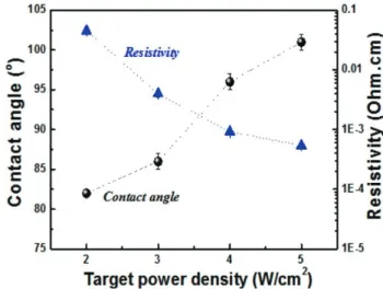
그림 5는 Ni 타겟 전력 밀도에 따라 증착된 C:Ni 박막의 접촉각과 비저항 값의 변화를 나타낸다. 결과에 서 보듯이 C:Ni 박막의 접촉각 값은 Ni 타겟 전력 밀도 증가에 따라 증가하였고, 비저항 값은 Ni 타겟 전력 밀도 증가에 따라 감소되었다. 이러한 결과는 박 막 내 금속 비율인 Ni 원자 비율이 증가되어 표면에너 지를 감소시키는 역할을 하였으며, 도핑된 금속 원자 증가로 인해 박막의 전도 특성이 향상되었다고 판단된 다. 결론적으로 Ni 타겟 전력 밀도 증가로 인해 증가 된 원자의 스퍼터링의 증가는 박막의 나노 결정화에 기여하게 되며, 박막 표면에서의 구조적 변화를 야기한 다고 판단할 수 있다 [6,11].
Fig. 5. Contact angle and resistivity values of C:Ni thin films deposited with the increase of Ni target power density.
Fig. 3. Rms surface roughness values of C:Ni thin films deposited with the increase of Ni target power density.
Fig. 4. Hardness and elastic modulus values of C:Ni thin films deposited with the increase of Ni target power density.
전기전자재료학회논문지, 제31권 제1호 pp. 40-43, 2018년 1월: 김광택 등 43
4. 결 론
본 논문에서는 비대칭 마그네트론 스퍼터링법으로 Ni 타겟 전력 밀도에 따라 증착시킨 Ni 도핑 탄소(C:
Ni) 박막의 표면, 구조⋅전기적 특성 등을 고찰하였다.
비대칭 스퍼터링 장치로 증착한 C:Ni 박막은 균일하 고 결함이 없이 증착되었으며, Ni 타겟 전력 밀도 증가 에 따라 표면 거칠기와 마찰계수 값은 감소하였다. C:
Ni 박막의 경도와 탄성계수 값은 전력 밀도에 따라 증 가하였고 박막의 비저항 값은 Ni 타겟 전력 밀도 증가 에 따라 감소하였다. 이러한 결과는 Ni 전력 밀도 증가 에 따라 비정질 탄소 박막에 금속인 Ni의 비율이 증가 하게 되고 이온화된 원자의 스퍼터링의 증가로 인해 향 상된 나노 결정화가 박막의 구조적 변화를 야기하였고, 물리적⋅전기적 특성 변화에 기여했다고 판단된다.
감사의 글
This research was supported by The Leading Human Resource Training Program of Regional Neo industry through the National Research Foundation of Korea (NRF) funded by the Ministry of Science, ICT and future Planning (grant number) (NRF-2016H1D5A1910658).
REFERENCES
[1] M. Dequaire, B. Limoges, J. Moiroux, and J. M. Savéant, J. Am. Chem. Soc., 124, 240 (2002). [DOI: https://doi.org/
10.1021/ja0170706]
[2] W. Lohmann and U. Karst, Anal. Chem., 79, 6831 (2007).
[DOI: https://doi.org/10.1021/ac071100r]
[3] Z. Dai, F. Yan, J. Chen, and H. Ju, Anal. Chem., 75, 5429 (2003). [DOI: https://doi.org/10.1021/ac034213t]
[4] L. H. Guo and N. Qu, Anal. Chem., 78, 6275 (2006).
[DOI: https://doi.org/10.1021/ac060351h]
[5] F. C. Walsh, Pure Appl. Chem., 73, 1819 (2001). [DOI:
https://doi.org/10.1351/pac200173121819]
[6] T. You, O. Niwa, Z. Chen, K. Hayashi, M. Tomita, and S. Hirono, Anal. Chem., 75, 5191 (2003). [DOI: https://doi.
org/10.1021/ac034204k]
[7] A. Grill, Thin Solid Films, 355-356, 189 (1999). [DOI:
https://doi.org/10.1016/S0040-6090(99)00516-7]
[8] C. H. Kiang, W. A. Goddard III, R. Beyers, and D. S.
Bethune, Carbon, 33, 903 (1995). [DOI: https://doi.org/
10.1016/0008-6223(95)00019-A]
[9] V. Kulikovsky, P. Bohac, F. Franc, A. Deineka, V.
Vorlicek, and L. Jastrabik, Diamond Relat. Mater., 10, 1076 (2001). [DOI: https://doi.org/10.1016/S0925-9635(00) 00525-2]
[10] A. Grill, Surf. Coat. Technol., 94-95, 507 (1997). [DOI:
https://doi.org/10.1016/S0257-8972(97)00458-1]
[11] A. Czyzniewski, Thin Solid Films, 433, 180 (2003). [DOI:
https://doi.org/10.1016/S0040-6090(03)00324-9]