Vol. 23, No. 12 (2013)
667
Hollow SnO
2Hemisphere Arrays for Nitric Oxide Gas Sensing
Hoang Nhat Hieu, Nguyen Minh Vuong and Dojin Kim
†Department of Materials Science and Engineering, Chungnam National University, 99 Daehak-ro, Yuseong-gu, Daejeon 305-764, Korea
(Received September 17, 2013 : Received in revised form November 6, 2013 : Accepted November 11, 2013)
Abstract We present an easy method of preparing two-dimensional (2D) periodic hollow tin oxide (SnO2) hemisphere array gas sensors using polystyrene (PS) spheres as a template. The structures were fabricated by the sputter deposition of thin tin (Sn) metal over an array of PS spheres on a planar substrate followed by calcination at an elevated temperature to oxidize Sn to SnO2 while removing the PS template cores. The SnO2 hemisphere array structures were examined by scanning electron microscopy and X-ray diffraction. The structures were calcined at various temperatures and their sensing properties were examined with varying operation temperatures and concentrations of nitric oxide (NO) gas. Their gas-sensing properties were investigated by measuring the electrical resistances in air and the target gases. The measurements were conducted at different NO concentrations and substrate temperatures. A minimum detection limit of 30 ppb, showing a sensitivity of S = 1.6, was observed for NO gas at an operation temperature of 150oC for a sample having an Sn metal layer thickness corresponding to 30 sec sputtering time and calcined at 600oC for 2 hr in air. We proved that high porosity in a hollow SnO2 hemisphere structure allows easy diffusion of the target gas molecules. The results confirm that a 2D hollow SnO2 hemisphere array structure of micronmeter sizes can be a good structural morphology for high sensitivity gas sensors.
Key words hollow hemispheres array, NO gas sensor, SnO2, low detection limit.
1. Introduction
Nitric oxide (NO) gas is a by-product of the combustion of substances in air, as in automobile engines and fossil fuel power plants. NO is also naturally produced during electrical discharges of lightning in thunderstorms. Nitric oxide rapidly oxidizes in air to nitrogen dioxide (NO2) to form photochemical smog and acid rain, which harm human health as an irritant gas causing respiratory in- fections.1) Thus, a sensor for detecting NO gas at low levels must be developed.
Gas sensors based on metal oxide semiconductors have been widely investigated in recent years. Among metal oxides, n-type tin oxide (SnO2) semiconductor is the predominant sensing material because of its low cost, excellent stability, and high sensitivity.2-3) The gas-sensing characteristics of this material markedly depend on its morphology and structure, such as porosity, grain size, surface-to-volume ratio, and shape. Accordingly, con- siderable efforts have been exerted to explore novel nano-
structured SnO2 materials, including nanotubes,4) nanorods,5,6) mesoporous and microporous structures,7,8) nanotriangles,9) and hollow nanospheres.10) The hollow-sphere structure may be a promising candidate nanostructure for high- performance gas sensors because of its high potential for encapsulating large quantities of gas molecules within the empty core domain. Indeed, some research groups have studied gas sensors with the form of hollow metal oxide spheres fabricated using templates such as carbon micro- sphere, polystyrene (PS) spheres, and spherobacteria.11-15) These morphologies exhibit high sensitivity to hydrogen, NO, NO2, hydrogen sulfide, methanol, etc.
Most fabrication methods are wet methods, i.e., they involve the absorption of metal ions in solution phase onto the functional surface layer of microspheres followed by calcination to form metal oxide hollow spheres. The process is fairly complicated and requires the development and accurate control of solutions. Moreover, the powders of synthesized hollow spheres have to be dispersed in a solvent to form slurry and then deposited onto substrates.
†Corresponding author
E-Mail : [email protected] (D. Kim, Chungnam Nat'l Univ.)
©Materials Research Society of Korea, All rights reserved.
This is an Open-Access article distributed under the terms of the Creative Commons Attribution Non-Commercial License (http://creative- commons.org/licenses/by-nc/3.0) which permits unrestricted non-commercial use, distribution, and reproduction in any medium, provided the original work is properly cited.
In practice, controlling the thickness of the sensing layer on a small sensor area is difficult. In this study, we reported an easy approach to preparing two-dimensional (2D) periodic SnO2 hollow hemisphere arrays for gas sensors. In this approach, PS spheres were used as template spheres, and then a tin (Sn) metal layer was sputter deposited onto the PS sphere template. Calcination at an elevated temperature was then performed to oxidize Sn while removing the template cores.
2. Experiment
PS spheres about 1µm in diameter were prepared according to the method in Ref.16) with some modifi- cations. Bar-type sensor electrodes were patterned on SiO2/ Si substrate with 5 mm× 5 mm dimensions by the dc sputtering of titanium (30 nm) and platinum (150 nm) in sequence through a metal shadow mask. A PS-sphere solution was formed by dispersing 1 wt% PS sphere powder in a mixture of water and ethanol (1:5). A few droplets of the PS-sphere solution were dropped onto the patterned substrate, followed by drying at 90oC for 5 min to form a multilayer of PS spheres on the substrate (Figs. 1a and 1b). The Sn metal layer was subsequently deposited onto the substrate by dc sputtering for 30 s using the Sn target (99.99 % purity) through a shadow mask (Fig. 1c). Notably, Sn metal was coated only on the top half of the stacked PS spheres because of the direc- tionality or shadowing effect of the sputtering method.
The prepared Sn/PS-sphere/SiO2/Si substrate was heated at 500oC for 2 h in an ambient-air furnace to burn out
the PS spheres while forming hollow spheres of SnO2
nanocrystallites. In the process, the SnO2 hollow hemi- sphere arrays collapsed down on the substrate (Fig. 1d).
Consequently, 2D a quasi-periodic SnO2 hollow hemi- sphere array structure was formed on the substrate for the NO sensor. The calcination temperatures were varied at 600, 700, and 800oC to find the highest response condition of the structure.
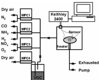
The morphology and crystalline properties of the samples were examined using field-emission scanning electron microscopy (FESEM; JEOL, JSM-700F) and X-ray dif- fraction (XRD; Rigaku D/MAX-RC) with Cu Kα radi- ation. Gas-sensing properties were investigated by mea- suring the electrical resistances in air (Ra) and target gases (Rg). The gas-sensing measurement system is depicted in Fig. 2 as reported in our previous work.17) Resistances were measured by applying a 2 V bias between the two electrodes while flowing gases into the chamber at a flow rate of 500 sccm. The response S of the gas sensor is defined by S = (Rg− Ra)/Ra. The measurements were con- ducted at different NO concentrations and substrate tem- peratures.
3. Results and discussion
Fig. 3(a) shows the typical morphology of the multi- layered PS spheres on SiO2/Si substrate. The PS spheres had a uniform average diameter of about 1µm. The morphology of 2D periodic SnO2 hollow hemisphere array structures that formed after combustion of the PS spheres is illustrated in Fig. 3(b). The inset shows the hollow voids in the SnO2 hemispheres. This hollow nature with a permeable wall of SnO2 enables the reaction gases to make contact with each other from both surfaces of the SnO2 layer. The XRD measurement results of SnO2 structures oxidized at different temperatures (500, 600, Fig. 1. Schematic of the fabrication procedure for 2D periodic
SnO2 hollow hemisphere arrays for gas sensors.
Fig. 2. Schematic of sensing measurement system.
700, and 800oC) are summarized in Fig. 3c. The peaks (110), (101), and (211) are indexed to the rutile lattice structure of SnO2 with lattice constants a = 4.738 Å and c = 3.188 Å (JCPDS file no. 41-1445).
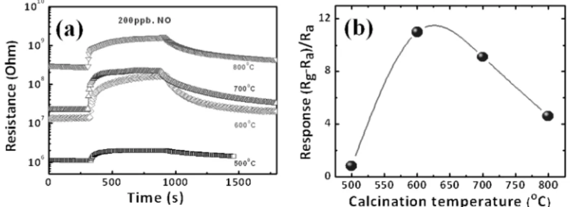
The sensing properties of the 2D hollow SnO2 hemi- sphere array sensors for NO gases diluted in dry air were then examined. Fig. 4 shows the measured sensing curves to 200 ppb NO gas for the sensors formed at different calcinations temperatures. The sensor response was the highest with the sensor calcined at 600oC showing a
sensitivity of S = 11 at an operation temperature 150oC.
Further increased calcination temperature lowered the response. Fig. 4(a) also shows that the resistance of the sensors increased with increased calcination temperature.
Given that the purpose of calcination was to oxidize Sn hemispheres in addition to burning the PS spheres, the crystalline structure and chemical stoichiometry of the formed SnO2 hemisphere layers determined the resistance.
The chemical stoichiometry or calcination-temperature dependence of the oxygen content in SnOx has been ob- Fig. 3. FESEM images of (a) PS spheres and (b) hollow SnO2 hemisphere arrays. Insets show high magnification views. (c) XRD patterns of hollow SnO2 hemisphere arrays structures formed at different calcination temperatures.
Fig. 4. (a) Response curves of sensor structures formed at different calcination temperatures to 200 ppb NO gas at 150oC and (b) summary of the responses.
Fig. 5. (a) Response curves of the sensor structure calcinced at 600oC to 200 ppb NO gas at different substrate temperatures and (b) summary of response vs. operation temperature.
served in our previous report with nanowire structure gas sensors in the form of SnOx single-wall carbon nanotube composites.17) In this previous study, x is found to approach 2 in SnOx upon oxidation at 600oC as the re- sistance increased. Therefore, the higher calcination tem- perature further completes the stoichiometry of SnO2 by removing the oxygen vacancies from the layer. This phenomenon could lead to low carrier concentration and poor sensing response.18,19) Grain growth with accom- panying resistance increase is also possible but may not be greater than the stoichiometric effect.
The effect of working temperature on the sensing re- sponse was also examined. Fig. 5 shows the responses of a sensor (600oC calcination) as a function of the operation temperature. The maximum response to NO gas was observed at 150oC, which was slightly lower than our previous optimum working temperature 200oC with SnOx single-wall carbon nanotube composites sensors17) and other SnO2 sensors for NO and NO2 gas detection.20-22) However, the response time was shorter at 200oC, as shown in Fig. 5(a). Therefore, the optimum operation temperature for the NO and/or NO2 gas sensors based on SnO2 semiconducting oxides was 150-200oC. Such mis- match between the operation temperatures for the maxi- mum response and for the fastest response has been observed.24) The response property of a resistive sensor at a given temperature is the sum of complex reactions, including ionosorption of oxygen, adsorption of NO, reaction and/or competition between NO and adsorbed oxygen ions, etc. Although each process can hardly be distinguished in practice, the final response level can measure the steady-state occupation of gases on the sur- face, whereas the response time measures how soon the steady state is reached. Considering that each thermally activated reaction process has different activation energies in principle, both the maximum response and the fastest response cannot occur at the same temperature. A ten- dency that the response time shortens at a higher tem- perature (200oC) can be due to the acceleration of
chemical reactions on the surface. However, the maximum response level could be obtained when the net adsorption rate (adsorption rate minus desorption rate of the total oxygen and NO gases under gas impingement) is higher at 150oC than at 200oC.
The sensor response as a function of NO gas concen- tration measured at the optimum operating temperature of 150oC is depicted in Fig. 6(a). Notably, the detection limit of the sensor to NO gas was as low as 30 ppb, showing a sensitivity of S = 1.6. This limit is the lowest among SnO2 sensors reported thus far. Furthermore, the 30 ppb concentration was the lowest NO concentration that the measurement system can feed because of the limitation of mass flow controllers and the NO gas mixture used. Fig. 6(b) compares the SnO2 hollow hemi- sphere sensor with a conventional thin lm type sensor for the response to 200 ppb NO gas at 150oC. These sensors were prepared under the same sputtering and calcination conditions. The sensitivity of SnO2 hollow hemisphere sensor (S = 11) was more than an order of magnitude higher than that of the thin film sensor (S = 0.4). The difference was partly due to the thin film sensor being unoptimized in contrast to the hollow hemisphere sensor.
For example, the thickness of the hemisphere sensor showed about half of the thin film for the same sputter deposition time because of the simple geometry (πr2 vs.
2πr2). The baseline resistance comparison in Fig. 6(b) revealed the difference. The thinner hemisphere structure would have higher resistivity and would show higher response if the thicknesses were greater than the total depletion condition.23,24)
4. Conclusions
A low-cost, easy fabrication process for 2D hollow SnO2 hemisphere array structures for highly responsive NO gas sensors was developed by sputtering Sn on arrayed PS spheres followed by oxidation. The sputter- deposited Sn on top of the PS spheres formed hemispheres Fig. 6. (a) Typical response curves of SnO2 hollow spheres to various concentrations of NO gas at 150oC, and (b) comparision of the sensitivity of SnO2 hollow half-sphere sensors with SnO2 thin lm sensor.
and collapsed down on the substrate while burning the PS spheres during calcination. The optimum operation tem- perature for the sensor made of SnO2 hollow hemisphere array structures was 150oC for the given Sn metal thick- ness and calcination at 600oC for 2 h in air. The lowest detection limit was 30 ppb NO concentration. The hemi- sphere morphology enabled a response of more than an order of magnitude higher than that of a thin-film type SnO2 sensor. This result, together with our previous finding on porous WO3 nanowire and ZnO urchin-like nanowire geometries, proved that high porosity in an ensemble of nanostructures and nanostructure geometries open to the exterior facilitated easy access of target gas molecules, thereby leading to high responses and low detection limits.
References
1. X. Han and L. P. Naeher, Environ. Int., 32, 106 (2006).
2. D. E. Williams, Sens. Actuators, B, 57, 1 (1999).
3. S. Basu and P. K. Basu, J. Sens., 2009, Article ID 861906 (2009).
4. G. X. Wang, J. S. Park, M. S. Park and X. L. Gou, Sens.
Actuators, B, 131, 313 (2008).
5. D. Wang, X. F. Chu and M. L. Gong, Sens. Actuators, B, 117, 183 (2006).
6. C. Zheng, Y. Chu, Y. Dong, Y. Zhan and G. Wang, Mater.
Lett., 59, 2018 (2005).
7. T. Hyodo, S. Abe, Y. Shimizu and M. Egashira, Sens.
Actuators, B, 93, 590 (2003).
8. G. Xi, Y. He, Q. Zhang, H. Xiao, X. Wang and C. Wang, J. Phys. Chem. C, 112, 11645 (2008).
9. R. G. Deshmukh, S. S. Badadhe, M. V. Vaishampayan and
I. S. Mulla, Mater. Lett., 62, 4328 (2008).
10. J. H. Lee, Sens. Actuators, B, 140, 319 (2009).
11. X. Sun, J. Liu, and Y. Li, J. Chem. Eur., 12, 2039 (2006).
12. T. Hyodo, K. Sasahara, Y. Shimizu and M. Egashira, Sens. Actuators, B, 106, 580 (2005).
13. J. Zhang, S. Wang, Y. Wang, Y. Wang, B. Zhu, H. Xia, X. Guo, S. Zhang, W.Huang and S. Wu, Sens. Actuators, B, 135, 610 (2009).
14. X. M. Yin, C. C. Li, M. Zhang, Q. Y. Hao, S. Liu, Q.H.
Li, L. B. Chen and T. H. Wang, Nanotechnology, 20, 455503 (2009).
15. L. He, Y. Jia, F. Meng, M. Li and J. Liu, J. Mater. Sci., 44, 4326 (2009).
16. H. N. Hieu, N. M. Vuong, H. Jung, D. M. Jang, D. Kim, H. Kim and S. -K. Hong, J. Mater. Chem., 22, 1127 (2012).
17. N. D. Hoa, N. V. Quy and D. Kim, Sens. Actuators, B, 142, 253 (2009).
18. G. -Y. Cha, A. H. Bui, W. -W. Baek, S. -T. Lee, D. -D.Lee and J. -S. Huh, Met. Mater. Int., 10, 149 (2004).
19. N. Barsan and U. Weimar, J. Electroceram., 7, 143 (2001).
20. C. D. Natale, F. Davide, G. Faglia and P. Nelli, Sens.
Actuators, B, 23, 187 (1995).
21. M. Egashira, Y. Shimizu, Y. Takao and S. Sako, Sens.
Actuators, B, 35, 62 (1996).
22. J. Santos, P. Serrini, B. O’Beirn and L. Manes, Sens.
Actuators, B, 43, 154 (1997).
23. N. M. Vuong, D. Kim, H. Jung, H. Kim, and S. K. Hong, J Mater Chem, 22, 6716 (2012).
24. H. N. Hieu, N. Q. Dung, J. Kim, and D. Kim, Nanoscale, 5, 5530 (2013).