Vol. 25, No. 9 (2015)
487
A Simulated Study of Silicon Solar Cell Power Output as a Function of Minority-Carrier Recombination Lifetime and Substrate Thickness
Kwang Su Choe
†Dept. of Electronic Materials Engineering, College of Engineering, The University of Suwon, Hwaseong-Shi, Gyeonggi-Do 445-743, Korea
(Received June 22, 2015 : Revised August 24, 2015 : Accepted August 24, 2015)
Abstract
In photovoltaic power generation where minority carrier generation via light absorption is competing against minority carrier recombination, the substrate thickness and material quality are interdependent, and appropriate combination of the two variables is important in obtaining the maximum output power generation. Medici, a two-dimensional semiconductor device simulation tool, is used to investigate the interdependency in relation to the maximum power output in front-lit Si solar cells. Qualitatively, the results indicate that a high quality substrate must be thick and that a low quality substrate must be thin in order to achieve the maximum power generation in the respective materials. The dividing point is 70µm/5 × 10−6 sec. That is, for materials with a minority carrier recombination lifetime longer than 5× 10⁻⁶ sec, the substrate must be thicker than 70µm, while for materials with a lifetime shorter than 5× 10⁻⁶ sec, the substrate must be thinner than 70µm. In substrate fabrication, the thinner the wafer, the lower the cost of material, but the higher the cost of wafer fabrication. Thus, the optimum thickness/lifetime combinations are defined in this study along with the substrate cost considerations as part of the factors to be considered in material selection.
Kye words
Si solar cell, minority-carrier recombination, substrate thickness, Medici, device simulation, solar cell efficiency.1. Introduction
In simple analogy, a solar cell is very much like a waterfall. That is, electrons are lifted to the conduction band by solar energy and then release the potential energy as they return to the valence band, just as water molecules are lifted to the air (vaporized) by solar energy and then release the potential energy as they return to the sea. Stiff potential gradients at pn junction and at waterfall itself allow a quick release of the potential energy that provides the driving force and kinetic energy for conduction electrons as well as water molecules. In this regard, one would make a great solar cell if all the attributes that make Niagara Falls a great waterfall are incorporated in solar cell design.
What are the common attributes to consider? First, a stiff (or abrupt) and high drop would cause the water to fall harder at the waterfall, while at the same time it would cause minority carriers (conduction electrons and holes) to separate swiftly at the pn junction. Second,
pores in the bedrocks would cause the water seep to the underground and thereby reduce the amount of water that actually reach the fall, while similarly active electron- hole recombination in the solar cell would reduce the number of free carriers flowing out of the cell. Third, debris blocking the free flow of water at the inlet and outlet of waterfall would reduce the amount of water flowing through waterfall, while similarly poor contacts at the semiconductor-metal junction would reduce the amount of electrical current reaching the load. Fourth, a dry weather with low precipitation would cause waterfall to wither, just as clouds or low winter daylights would reduce the power output of solar cell. With a little im- agination, one may go on naming more common attributes of waterfall and solar cell. This solar cell-waterfall analogy given, of course, is neither perfect nor complete.
Nonetheless, it gives a visual image, by way of a waterfall, of a solar cell whose interior working is invisible to human eyes and has been previously left to theoretical and mathematical descriptions.
†Corresponding author
E-Mail : [email protected] (K. S. Choe, Univ. of Suwon)
©Materials Research Society of Korea, All rights reserved.
This is an Open-Access article distributed under the terms of the Creative Commons Attribution Non-Commercial License (http://creative- commons.org/licenses/by-nc/3.0) which permits unrestricted non-commercial use, distribution, and reproduction in any medium, provided the original work is properly cited.
In regards to the most popular Si solar cells, the highest efficiency reported to date for an actual cell is 24.7 % by a method known as PERL (Passivated Emitter, Rear Locally-diffused).
1)More typical value accepted in labora- tory-scale solar cells is about 20 %, or 20 mW·cm
−2under AM1.5.
2)This is because of the fact that the energy of the photons that are directly responsible for electron-hole generation accounts for less than 30 %, in case of the Si solar cell, of the total energy of the incoming photons
3)and that the electron-hole pairs generated by light absorption are lost to recombination before being able to flow out of the solar cell and pass through the load. The minority-carrier recombination, just as the water seepage through porous bedrocks, is a material issue and will become even more serious as the material is downgraded from the nearly defect-free mono-crystalline silicon to defect-ridden polycrystalline or amorphous silicon.
Under light absorption, immobile electrons in the valence band are elevated to the conduction band resulting in free electron (in the conduction band) and hole (in the valence band) pairs. The free electrons generated in the p-type side and holes generated in the n-type side of the pn junctions are minority carriers that are very prone to recombination with much more abundant majority carriers, i.e., holes in the p-type side and electrons in the n-type side. Although the minority-carrier recombination mechanisms are beyond the scope of this discussion, it is generally understood that the recombination is accelerated by the presence of impurities and defect sites in the substrate material. In this regards, the crystalline quality and doping levels are relevant factors. The overall measure of the effects of these factors is expressed in minority- carrier recombination lifetime, i.e., the time it takes for an electron-hole pair to recombine after its generation (formation.). Another related issue deals with the substrate thickness as it determines the distance the minority carriers have to travel before exiting the solar cell.
In Si solar cell production, the wafer substrate is an important cost factor, due to the cost of material itself and the cost of wafer fabrication: The thinner the wafer, the lower the cost of material, but the higher the cost of wafer fabrication. In addition, a shorter minority-carrier recombination lifetime (poorer material quality) requires a proportionately thinner wafer. In this regard, the opti- mum substrate thickness is not one fixed value, but variable depending on the material quality and the cost.
As the material cost consideration encourages the switch from more expensive float-zone or Czochralski mono- crystalline silicon to a variety of less expensive polycry- stalline silicon, the substrates obviously need to be made thinner in order to deal with the minority-carrier recom- bination issue. As to exactly how much, as well as the inter-relationship between minority-carrier lifetime and
substrate thickness as they together affect the quantum efficiency, is a question that can only be answered by repetitive experiments that are yet to be conducted com- prehensively. In this work, computer simulations were con- ducted in lieu of laboratory experiments by using Medici, 2-dimensional semiconductor device simulation software.
Despite the virtual nature of computer simulation, the results should prove to be useful in better understanding the substrate issues and serving as a guide in determining the proper substrate quality/thickness combinations.
2. Experimental
As a substitute for laboratory experiments, computer simulation is useful in situations that call for repeated measurements with incremental changes in a variable or variables. Particularly when the independent variables are more than one and inter-related, the situation can be very complex, and the simulation may be the only practical option that is next to the real thing. Just as in a modeled house where essential features of a real house is con- structed, viewed and tested before the actual structure is built at great expense and time, in computer device simulation similar constructing, viewing and testing are all done in the virtual space.
The Medici simulation consists of four major steps.
First, the solar cell structure is formed by grids or mesh, a sort of like building a modeled house using match sticks. The regions near the front and back surfaces and at the pn junction where active photo-generation and carrier recombination occur are finely meshed, and the bulk region deep in the body of the solar cell, where the electrical activities are relatively minor, are coarsely meshed to save computation time. Each type of the n- and p-type regions is then doped to a desired level. Second, the physical models relating to the operation of the solar cell and mathematical models and methods relating to nu- merical calculations are each specified. Third, the solutions are reached by iterative numerical calculations. Fourth, the simulation results or the outputs are accessed in text, graph or the pictorial form.
The solar cell chosen for the simulation study is a front-lit structure of p-type silicon substrate. A standard back-lit grid structure in the Medici operational manual
4)is modified to meet the front-lit structural requirements.
In this 2-dimensional front-lit structure, the substrate, the
thickness of which is an independent variable, is doped
p-type in the concentration of 1 × 10
14cm
−3. Laterally, only
a 10 μm segment of the substrate is chosen to conserve
the simulation time. The n-type emitter on top is doped
to the concentration of 1 × 10
17cm
−3. The location of the
pn junction, between the emitter and the substrate, or
base, is 2 μm below the front surface. The front metal
contact finger is placed in the middle of the modeled structure and 1 μm in width. The back metal contact covers the full area of the back surface. This structure was used successfully in earlier works concerning front-lit vs. back-lit solar cells
5)and the back-surface field (BSF) effects.
6)In regards to model and parameter selection, Auger and concentration-dependent Shockley-Read-Hall recom- bination models and a concentration-dependent mobility model are chosen. The 2-carrier Newtonian iteration is chosen as the mathematical model in solving the governing equations by finite element analysis. The minority-carrier lifetime, another independent variable, is assumed to be identical for both electrons and holes. Lastly, except for the parameters that are chosen, default values are used.
The photo-generation rate, electron-hole-pairs·cm
−3·s
−1, is an exponential function of distance y from the surface and can be expressed as:
(Eq. 1) where FLUX is defined as the photon flux (photons·
cm
−2·s
−1) and Y.CHAR is defined as the absorption dis- tance ( μm).
4)The photon absorption is strongly frequency- dependent. That is, the higher the frequency, or the shorter the wavelength, the stronger the photon absorption and therefore the shorter the absorption distance. For the present simulation experiments, the wavelength of 0.6 μm, the peak point in the AM1.5 spectrum having an ab- sorption distance of 2 μm, is chosen for the incident photons. The photon flux is set at 4 × 10
17cm
−2·sec
−1. For these absorption distance and photon flux, the Eq. (1) can be rewritten as:
(Eq. 2) Finally, after the simulation, the output is plotted in terms of the photovoltaic equation as expressed in:
(Eq. 3) From the I-V curve plotted, the open-circuit voltage, V
oc, is extracted from where the curve intersects the x- axis, and the short-circuit current, I
sc, is extracted from where the curve intersects the y-axis. The cell power as defined by the maximum power rectangle in the loaded circuit is then extracted.
3. Results and Discussion
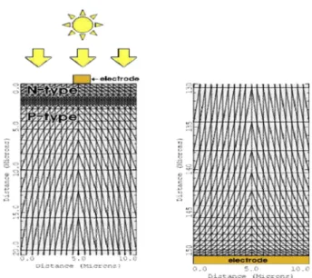
Fig. 1 illustrates the grid structure, formed by Medici, of a front-lit Si solar cell under study, consisting of an n-
type emitter on a p-type base. The left shows the top 20 μm of the structure: the np junction is located 2 μm from the top surface. The right shows the bottom 20 μm of the structure. The grids are dense near the top and bottom surfaces and at the junctions where changes, in terms of electrical activities and doping concentrations, are large and sparse in the bulk where the changes are small. The grid structure is fixed except for the height, corresponding to the substrate thickness, in the y direction. The sub- strate thickness is an independent variable ranging from 10 μm to 150 μm. The other independent variable is minority-carrier lifetime which is assumed to be the same for both electrons and holes and ranges from 5 × 10
−1sec to 5 × 10
−10sec.
The visual relationship between the two independent variables, substrate thickness in the x-axis and minority- carrier recombination lifetime in the y-axis, and a de- pendent variable, the maximum solar cell output power in the z-axis, in a loaded front-lit Si solar cell is illustrated in Fig. 2. In regards to the recombination lifetime, little difference is observed when the time deceases from 5 × 10
−1sec to 5 × 10
−5sec. The output power stays nearly constant at the maximum value of about 2.0 × 10
−2W·cm
−2, or 20 mW·cm
−2as the substrate thickness is reduced from 150 μm to 80 μm and then decreases expo- nentially as the thickness is further reduced down to 10 μm. Thus for high quality mono-crystalline silicon with a recombination lifetime of longer than 5 × 10
−5sec, minority-carrier recombination is not a major issue up to the 150 μm substrate thickness, but the loss of light absorption can become increasingly a larger issue if the
Gphoton FLUX
y Y.CHAR– --- exp
10–4×Y.CHAR ---
=
Gphoton 2 10× 21e2 µm---–y
cm–3–sec–1
=
I = Io⎝⎛eqVkT---–1⎠⎞ I– sc
Fig. 1. A typical 2-dimensional grid structure of a front-lit solar cell rendered by Medici.4) The left shows top 20µm: the emitter- base np junction is located 2µm below the top surface. The right shows bottom 20µm.
substrate thinned below 80 μm. On the other hand, when the minority-carrier recombination lifetime is shorter than 5 × 10
−5sec, the minority-carrier recombination also comes into play significantly and competes against the light absorption. As such, there exists an optimum substrate thickness for each recombination lifetime that would give the maximum power output, i.e., 70 μm for 5 × 10
−6sec to give 20.2 mW·cm
−2, 40 μm for 5 × 10
−7sec to give 19.4 mW·cm
−2, 20 μm for 5 × 10
−8sec to give 17.5 mW·cm
−2, 10 μm for 5 × 10
−9sec to give 13.4 mW·cm
−2, and 10 μm for 5 × 10
−10sec to give 6.0 mW·cm
−2. For the last two combinations, the power output may be even higher, if the substrate were made thinner than 10 μm which was the experimental lower limit in this study.
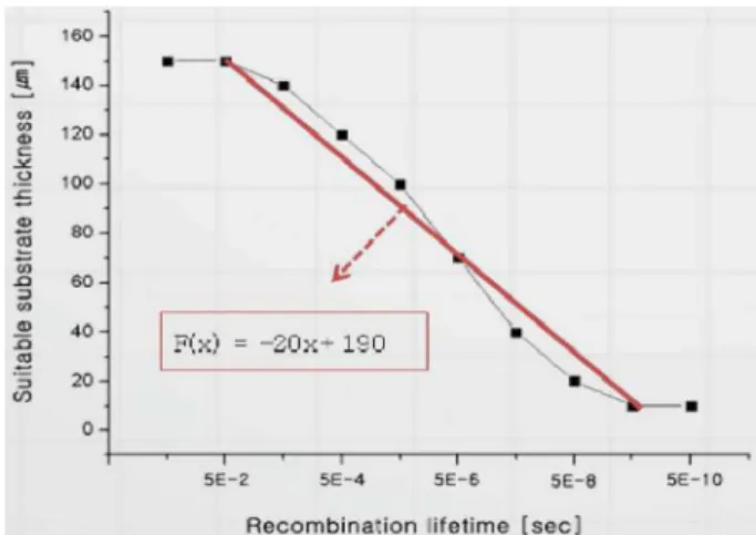
The substrate thickness/minority-carrier recombination lifetime combinations that would give the maximum power output are plotted in Fig. 3. The inverse relationship between substrate thickness and minority-carrier recom- bination lifetime generally holds from the latter values of 5 × 10
−2sec down to 5 × 10
−9sec. An inflection point exists at the 70 μm/5 × 10
−6sec combination: above which the slope is more gradual and below which stiffer. This indicates that the effect of minority-carrier recombination gets increasingly more negatively pronounced as the lifetime gets shorter than 5 × 10
−6sec such that the sub- strate has to be thinned to a greater extent to minimize the negative effect. From the figure, one may infer that at the current state-of-the-art 50 μm substrate thickness the power output would not suffer losses as long as the lifetime is 1 × 10
−6s or longer. A straight line fit of the curve yields
F(x) = −20x + 190 (Eq. 3)
where F(x) ≡ substrate thickness for the maximum power output, μm; x ≡ exponent value of the minority-carrier recombination lifetime.
This approximate equation may be used as a rough guideline in determining the appropriate substrate thick- ness when the quality of material, as quantified by the minority-carrier recombination lifetime, is known. The linear regression analysis of the entire data points, on the other hand, yields F(x) = −18.848x + 184.67 and R
2= 0.9613.
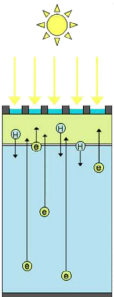
How minority-carrier recombination lifetime and sub- strate thickness affect the solar cell power output is visualized in Fig. 4, where holes are the minority carriers in the n-type emitter on top and electrons are the minority carriers in the p-type base. As the n-type emitter is relatively thin, even a very short recombination lifetime would allow the holes to drift into the p-type base, while the p-type base is much thicker and would require a much longer recombination lifetime to allow electrons sufficient time to travel the long distances from the generation sites in the base to the emitter layer. There- fore, for a solar cell with p-type base or substrate, as is the case in this study, the electron recombination lifetime would be the variable that determines the maximum substrate thickness, while the hole recombination lifetime would dominate if an n-type substrate were to have been used instead.
In summary, a standard front-lit Si solar cell was examined by Medici, a simulation software tool, to deter- mine the effect of the variations in substrate thickness and minority-carrier recombination lifetime on the solar cell power output. For high-quality (long recombination
Fig. 3. Substrate thickness/recombination lifetime combinations that yield the maximum power output. The maximum power values are the peak points in the z-axis of Fig. 2. In the linear-fit equation, x is the exponent of recombination lifetime, and F(x) is substrate thickness (µm).Fig. 2. A 3-dimensional illustration of experimental results:
substrate thickness in the x-axis, minority-carrier recombination lifetime in the y-axis, and solar cell output power in the z-axis.
lifetime) substrates, a maximum power output was achieved with a relatively thick substrate, while the situation is opposite for poor-quality (short recombination lifetime) substrates. In this regard, the substrate thickness/recom- bination lifetime combination of 70 μm/5 × 10
−6sec is found to the point dividing the high- and poor-quality regions.
4. Conclusion
Recombination of minority carriers is a major contri- buting factor in loss of quantum efficiency and output power in solar cells. As minority-carrier generation by light absorption is competing against minority-carrier re- combination, substrate thickness and material quality are interdependent, and a proper combination of the two variables is important in ultimately leading to the maxi- mum output power generation. Medici, a 2-dimensional
semiconductor device simulation tool, was used to study the interdependency in relation to the maximum power output in front-lit Si solar cells. Qualitatively speaking, the results indicate that a high-quality substrate needs to be made thick and that a low-quality substrate, thin in order to achieve the maximum power generation in the respective material. The dividing point is found to be 70 μm/5 × 10
−6sec. That is, for materials with a minority- carrier recombination lifetime longer than 5 × 10
−6sec, the substrate needs to be thicker than 70 μm, while for materials with the lifetime shorter than 5 × 10
−6sec, the substrate needs to be thinner than 70 μm. Specifically, for the standard 150 μm substrate thickness the power output stays nearly at the maximum value of about 2.0 × 10
−2W·cm
−2, or 20 mW·cm
−2, as long as the recombination lifetime is 5 × 10
−5s or longer, while at the current state- of-the-art 50 μm substrate thickness, on the other hand, the power output would not suffer any loss as long as the lifetime is 1×10
−6s or longer. This means that the push for cheaper material with poorer quality can be accom- plished as long as it is accompanied by advances in wafer or substrate thinning technologies. In practice, the thinner the wafer, the lower the cost of material, but the higher the cost of wafer fabrication. Thus, the optimum thickness/lifetime combinations defined in this study can be useful in making right material selection.
Acknowledgement
The simulation experiments and the rendering of the graphical work were assisted by undergraduate students, Messrs. Sei-Chan Kim, Jun-Sik Moon, Jun-Won Suh, Yun-Jei Lee, Young-Jun Joh, Ji-Ju Lee, Houng-Jun Jung, and Sung-Sik Hwang of the Department of Electronic Materials Engineering of the University of Suwon. The author wishes to thank them for the diligent work as well as the shared good times.
References
1. M. A. Green, K. Emery, D. L. King, Y. Hishikawa and W. Warta, Prog. Photovolt. Res. Appl., 15, 35 (2007).
2. J. H. Kim, M. J. Chu, Y. D. Chung, R. M. Park and H. K.
Sung, Electron. Telecommun. Res. Inst., 23, 2 (2008) (in Korean).
3. F. Dimorth and S.Kurtz, MRS Bull., 32, 230 (2007).
4. Medici Two-Dimensional Device Simulation Program, Ver. 2.2, User's Manual, vol. 3, Technology Modeling Associates, Inc., Sunnyvale, CA, Jun. 1996, pp. 7.1-7.10.
5. K. S. Choe, Solid State Sci., 12, 1948 (2010).
6. K. S. Choe, Solid State Sci., 29, 48 (2014).
Fig. 4. Description of minority carriers: holes in the n-type emitter and electrons in the p-type base. As the base region is almost as thick as the substrate itself, the electrons have much longer distance travel to the pn junction and thus require a longer lifetime when the substrate is thicker.