• 검색 결과가 없습니다.

Switched-Capacitor Based Digital Temperature Sensor Implemented in 0.35-µm CMOS Process

N/A
N/A
Protected

Academic year: 2021

Share "Switched-Capacitor Based Digital Temperature Sensor Implemented in 0.35-µm CMOS Process"

Copied!
4
0
0

로드 중.... (전체 텍스트 보기)

전체 글

(1)

21 J. Sensor Sci. & Tech. Vol. 27, No. 1, 2018 Journal of Sensor Science and Technology

Vol. 27, No. 1 (2018) pp. 21-24 http://dx.doi.org/10.5369/JSST.2018.27.1.21 pISSN 1225-5475/eISSN 2093-7563

Switched-Capacitor Based Digital Temperature Sensor Implemented in 0.35- µm CMOS Process

Su-Bin Kim, Jeon-Woong Choi, Tae-Gyu Lee, Ki-Ppeum Lee, and Hang-Geun Jeong

Abstract

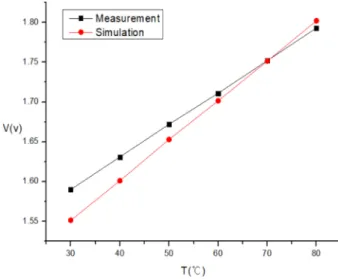
A temperature sensor with a binary output was implemented using switched-capacitor circuits in a 0.35-µm CMOS(com-plementary metal-oxide semiconductor) process. The measured temperature exhibited good agreement with the oven temperature after calibration.

The measured power consumption was 5.61 mW, slightly lower than the simulated power consumption of 6.63 mW.

Keywords: Temperature sensor, Switched-capacitor, Sigma-delta modulator, Charge balancing

1. INTRODUCTION

CMOS temperature sensors with digital outputs are widely used because of their low cost and ease of interfacing with digital systems[1]. Digital CMOS temperature sensors can be implemented using different methods. Among them, switched- capacitor-based circuits have the advantage of small chip area and low power consumption because resistors can be eliminated[2-3].

One approach of designing such a switched-capacitor-based temperature sensor was discussed in [4]. This paper presents the measurement results of the temperature sensor fabricated in a 0.35- μm CMOS process.

This paper is organized as follows: Section 2 reviews the operating principle for the digital CMOS temperature sensor.

Section 3 briefly reviews the sensor implementation. The chip test methods and measurement results are discussed in Section 4.

Finally, conclusions are drawn in Section 5.

2. PRINCIPLE OF OPERATION 2.1 Temperature sensing

In a forward-biased diode, the diode voltage, can be expressed as a function of the diode current, and the temperature, as shown in (1):

, (1)

where k is the Boltzmann constant, q is the charge of the electron, T is the absolute temperature, and I

s

is the saturation current of the diode. In (1), the thermal voltage, kT/q is proportional to the temperature, but the saturation current increases exponentially with temperature, which overwhelms the proportionality of the thermal voltage. Thus, the diode voltage decreases with temperature, exhibiting CTAT (complementary to absolute temperature) charac-teristics[5].

To use the temperature proportionality of the thermal voltage, the temperature dependence of the saturation current should be eliminated. If we use two diodes with different current densities and take the difference between the two diode voltages, we can cancel the saturation current effect, as shown in (2):

, (2)

where p is the current density ratio between the two diodes. Thus, the differential voltage defined in (2) is proportional to the temperature and is called the PTAT (proportional to absolute temperature) voltage[5].

For temperature measurement, we can use an external voltmeter and perform the calculation to obtain the temperature, or we can build an internal reference voltage for a direct temperature output without using an external voltmeter. The reference voltage can be generated by adding a slope-adjusted PTAT voltage to the CTAT

V

D

I

D

V

D

kT --- q I

D

I

S

ln ----

=

V

D

≡ V

D2

– V

D1

Δ kT

--- q ln ( ) p

=

Department of Electronic Engineering, Chonbuk National Unversity College of Engineering, Chonbuk National University, 567 Baekje-daero, Deokjin-gu, Jeollabuk-do 561-756, Korea

+

Corresponding author: [email protected] (Received: Jan. 11, 2018, Accepted: Jan. 29, 2018)

This is an Open Access article distributed under the terms of the Creative Commons Attribution Non-Commercial License(http://creativecommons.org/

licenses/bync/3.0) which permits unrestricted non-commercial use, distribution,

and reproduction in any medium, provided the original work is properly cited.

(2)

Su-Bin Kim, Jeon-Woong Choi, Tae-Gyu Lee, Ki-Ppeum Lee, and Hang-Geun Jeong

J. Sensor Sci. & Tech. Vol. 27, No. 1, 2018 22 voltage, such that the magnitudes of the positive and negative slopes cancel each other, resulting in the BGR (bandgap reference) voltage, as shown in Fig. 1.

To determine the temperature, we can use the normalized voltage, defined as the ratio of the PTAT voltage to the BGR voltage, as in (3).

Normalized Voltage = , (3)

Because the BGR voltage is always 1.2V, regardless of temperature, the nomalized voltage value is between 0 and 1, depending on the temperature. If the normalized voltage is 0, it means that the absolute temperature is 0 K; and when it is 1, it means that it is 600 K. Thus, we can simply obtain the temperature by multiplying the normalized voltage by 600.

2.2 Analog to digital conversion

A sigma-delta modulator can be used to obtain a digital output for the measured temperature[6,7]. The sigma-delta modulator is implemented using the charge-balancing principle, as shown in Fig. 2.

The feedback action forces the output of the accumulator toward 0 by subtracting the VCTAT for a positive output and by

adding the VPTAT for a negative output. This results in charge balance, as expressed by (4):

, (4)

where is the number of “1” bits, is the number of “0” bits.

3. SENSOR IMPLEMENTATION

The design of the CMOS temperature sensor is discussed in detail in [3]. The block diagram of the temperature sensor is shown in Fig. 3.

Fully differential structures are used to eliminate charge injection and clock feedthrough in switched-capacitor circuits.

Fig. 4 shows the layout of the entire circuit of the temperature PTAT

PTAT CTAT + --- PTAT

--- BGR

=

N

1

CTAT = N

0

PTAT

N

1

N

0

Fig. 1. Generation of bandgap reference voltage

Fig. 2. Chargebalancing principle

Fig. 3. Charge-balancing temperature sensor

Fig. 4. Temperature sensor layout

(3)

Switched-Capacitor Based Digital Temperature Sensor Implemented in 0.35- µm CMOS Process

23 J. Sensor Sci. & Tech. Vol. 27, No. 1, 2018 sensor. The size is approximately 550 μm × 600 μm.

The simulated density of “1” of the temperature sensor is shown in Fig. 5. The number of “1” bits of the output data (for a duration of 15 ms) is plotted as a function of the temperature. The density of “1” bits increases almost linearly as the temperature increases.

4. MEASUREMENT

4.1 Test board design

To digitally display the temperature, we need a decimation filter. However, we used a simple, passive LPF (low-pass filter) for convenience, as shown in Fig. 6. To determine the time constant of the LPF, we assumed that 1600 bits are adequate for the proper averaging of the sigma-delta modulation output. Thus, the required time constant is RC=10 μ(s) × 1600 = 0.016 (s).

Therefore, we used a resistor (R2) of 16 kΩ and a capacitor (C2)

of 1 µF to make a time constant of 0.016 (s).

R1 is a resistor for impedance matching with Rs, which is the internal output impedance of the function generator. C1 is a capacitor for the power-supply decoupling.

The chip was fabricated using the 0.35- μm process from Magna-chip Semiconductor. Fig. 7 shows a PCB board with the chips and additonal circuitry.

A spectre simulation was performed to verify the measurement setup.

We checked the output voltage for the temperature range from 30 °C to 80 °C at 10 °C intervals. The simulation results are shown in Table. 1.

4.2 Chip test

We measured the output voltage for the temperature range from 30 °C to 80 °C at 10 °C interval using a temperature oven. The measured data are shown in Table 2.

Fig. 5. Number of “1” vs. temperature

Fig. 6. Board design for chip test

Fig. 7. PCB board for chip test

Table 1. Spectre simulation results

Temperature(°C) Voltage(V) Difference(V)

30 1.551 -

40 1.601 +0.050

50 1.653 +0.052

60 1.701 +0.048

70 1.751 +0.050

80 1.802 +0.051

Table 2. Chip test results

Temperature(°C) Voltage(V) Difference(V)

30 1.590 -

40 1.631 +0.041

50 1.672 +0.041

60 1.711 +0.039

70 1.752 +0.041

80 1.793 +0.041

(4)

Su-Bin Kim, Jeon-Woong Choi, Tae-Gyu Lee, Ki-Ppeum Lee, and Hang-Geun Jeong

J. Sensor Sci. & Tech. Vol. 27, No. 1, 2018 24 In Fig. 8, the measured data are compared against the simulated data. A difference was present in the average slope between the measurement (0.00406V/K) and the simulation (0.00501V/K).

To determine the cause of the discrepancy, the finalized circuit and layout was scrutinized. The discrepancy was found to be due to the mismatch in the slopes of the PTAT and CTAT voltage, which occurred in the finalized circuit because of the error between the two versions of the designed circuits. In the fabricated circuit, the PTAT slope was 1.91 mV/K, while the CTAT slope was -1.8 mV/K, with a slighly mismatched slope

The measured power consumption of the temperature sensor was 5.61 mW, while the simulated power consumption was 6.63 mW.

5. CONCLUSIONS

A switched-capacitor-based CMOS temperature sensor with digital output was fabricated in a standard 0.35-μm CMOS process. The measured temperature is in good agreement with the oven temperature after calibration. The discrepancy in the slope between the simulation and the measurement was found to be attributable to the error in the designed circuit versions during the chip design process. The measured power consumption was 5.61 mW, showing the feasibility of low-power operation.

REFERENCES

[1] M. Pertijs and J. H. Huijsing, Precision Temperature sen- sors in CMOS Technology, Springer, Dordrecht, pp. 180- 182, 2006.

[2] B. Razavi, Design of Analog CMOS Integrated Circuits, McGraw-Hill, New York, pp. 395-438, 2000.

[3] A. Danchiv, M. Bodea, and C. Dan, “A fully differential switched capacitor amplifier modelling and parameter eval- uation”, Infineon Technologies Romania Blvd, pp. 1-6, Bucharest, Romania. 2014.

[4] J. Hang-Geun, S. Bich, P. Byeong-Jun, G. Gwang-Hoe, C.

Dae-Eun, P. Hueon-Beom, “Digital CMOS temperature sensor implemented using switched-capacitor circuits”, Journal of Sensor Science and Technology, pp. 326-332, 2016.

[5] http://www.uio.no/studier/emner/matnat/ifi/INF4420/v12/

undervisningsmateriale/INF4420_02_Bandgaps_Print.pdf (retrieved on Dec, 28, 2017)

[6] R. Schreier and G. C. Temes, Understanding Delta-Sigma Data Converter, John Wiley & Sons, New York, pp. 4-10, 2004.

[7] P. Sang-Il, Principles of Sigma-Delta Modulation for Ana- log-to-Digital Converters, Motorola, pp. 5.1-6.13, 1990.

Fig. 8. Measurement vs. simulation

수치

Fig. 2. Chargebalancing principle
Fig. 5. Number of “1” vs. temperature
Fig. 8. Measurement vs. simulation

참조

관련 문서

produces a magnetic field which can be guided by a magnetic yoke to a linear Hall sensor; the output of the sensor is proportional to the electric current..

The index is calculated with the latest 5-year auction data of 400 selected Classic, Modern, and Contemporary Chinese painting artists from major auction houses..

The key issue is whether HTS can be defined as the 6th generation of violent extremism. That is, whether it will first safely settle as a locally embedded group

The “Asset Allocation” portfolio assumes the following weights: 25% in the S&P 500, 10% in the Russell 2000, 15% in the MSCI EAFE, 5% in the MSCI EME, 25% in the

1 John Owen, Justification by Faith Alone, in The Works of John Owen, ed. John Bolt, trans. Scott Clark, "Do This and Live: Christ's Active Obedience as the

In order to analyze thermal stability and capacity loss according to the temperature of the battery cell by applying different C-rate discharge and

In gi ngi va,LCs are found i n oralepi thel i um ofnormalgi ngi va and i n smal l er amountsi nthesul cul arepi thel i um,buttheyareprobabl yabsentfrom thejuncti onal epi thel

( Thermal runaway: a phenomenon that occurs when the power dissipation of the output stage brings temperature rise to the output stage brings temperature rise to the