Research on In-band Spurious Evasion Techniques of Hybrid Frequency Synthesizer
Seung-Woo Kim
*★, Woo-Sung Yoo
**Abstract
The study aims to a design hybrid frequency synthesizer in spectrum analyzer and to propose new techniques designed for evasion of in-band spurious. The study focuses on calculating the exact location of multiple phase locked loop of hybrid frequency synthesizer and spurious of direct digital synthesizer to evade in-band spurious outside of frequency range that the user wants to see and thereby simulating technique to improve input related spurious of spectrum analyzer for algorithm. The proposed technique is designed to calculate spurious evasion algorithm in central processing system when in-band spurious arises, and to move output frequency of DDS(direct digital synthesizer) into the place where no in-band spurious exists thereby improving performance of frequency synthesizer. The study used simulation and result representation to prove the effectiveness of the proposed technique.
Key words: In-band Spurious, Phase Locked Loop Reference Spurious, Direct Digital Synthesizer Spurious, Hybrid Frequency Synthesizer, DDS Driven Frequency Synthesizer.
* Defense Agency for Technology and Quality
** LIGNex1
★Corresponding author
Email :[email protected], Phone : 054-475-0746
※ Acknowledgment
Manuscript received Feb. 9, 2015; revised May. 12, 2015
; accepted May. 13. 2015
This is an Open-Access article distributed under the terms of the Creative Commons Attribution Non-Commercial License(http://creativecommons.org/licenses/by-nc/3.0) which permits unrestricted non-commercial use, distribution, and reproduction in any medium, provided the original work is properly cited.
I. Introduction
Frequency synthesizer is widely used for modern communication systems. With the advance in wireless mobile communication, more attention is being paid to frequency synthesizer[1].
Usually spectrum analyzer is composed as 3-stage super heterodyne receiver. 1st local oscillator is using the YTO(YIG Tuned Oscillator), due to the ensuring a wide frequency range and excellent phase noise performance. 2nd local oscillator and 3rd
local oscillator produce fixed frequency.
Frequency synthesizer used for spectrum analyzer must produce frequency ranging between 3.0GHz and 7.0GHz in the area of RF frequency as well as good quality phase noise and spurious. Also, frequency resolution must be below 1 Hz. These characteristics affect lock settling time, sweep time, frequency accuracy and dynamic range in the spectrum analyzer[2],[3].
PLL(Phase Locked Loop) frequency synthesizer gets reference spurious to be close to output frequency of synthesizer due to low reference frequency. Thus, loop filter design is very important, raising the need to resolve shortcomings resulting from increasing lock time. To get over the shortcomings, the frequency synthesizer in spectrum analyzer, in many cases, uses hybrid frequency synthesizer feature like DDS(Direct Digital Synthesizer) and PLL to secure resolution of fewer than 1Hz and to satisfy conditions for high-speed lock Time and sweep time[4]. But even with the hybrid frequency synthesizer feature like DDS and PLL cannot avoid reference spurious[5].
This study proposes a new technique designed to evade in-band spurious arising from reference spurious of hybrid frequency synthesizer. By presenting mathematic modeling regarding reference frequency scheme of frequency synthesizer, the study proposed evasion algorithm for in-band spurious and then verified result of application involving proposed evasion technique.
Ⅱ. Hybrid Frequency Synthesizer Hardware Configuration
Frequency synthesizer involving phase locked loop is designed to diffuse output frequency of oscillator and then to bring feedback to input table for comparison and synchronization with reference frequency. By changing diffusion rate, you can change output frequency. The method is used by most of frequency synthesizer due to its flexibility and adaptability of the circuit the method utilizes.
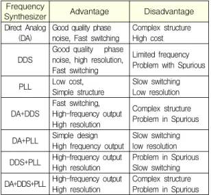
This technique has an advantage of simplified circuit design and a good reference frequency. But switching time and resolution are bad. Table 1 shows advantage and disadvantage of frequency synthesizer[6],[7].
Table 1. Comparison of frequency synthesis Frequency
Synthesizer Advantage Disadvantage Direct Analog
(DA) Good quality phase
noise, Fast switching Complex structure High cost DDS Good quality phase
noise, high resolution, Fast switching
Limited frequency Problem with Spurious PLL Low cost,
Simple structure Slow switching Low resolution DA+DDS Fast switching,
High-frequency output High resolution
Complex structure Problem in Spurious DA+PLL Simple design
High frequency output Slow switching low resolution DDS+PLL High-frequency output
High resolution Problem in Spurious Slow switching DA+DDS+PLL High-frequency outputHigh resolution Complex structure
Problem in Spurious
Spectrum analyzer used multiple locked loop, DDS and DA(Direct Analog) to secure appropriate phase
noise and resolution of fewer than 1Hz but it also employed sampling mixer featuring SRD(Step Recovery Diode) for comparison with frequency reaching between 3.0GHz and 7.0GHz. In addition, it also used 14-bit DDS to satisfy frequency resolution and good quality phase noise [8],[9].
Fig. 1. Frequency synthesizer block diagram Fig. 1 shows block diagram of hybrid frequency synthesizer in spectrum analyzer.
Ⅲ. Frequency Synthesizer : Theory and Design
As described in Fig. 2. and Fig. 3. both PLL and DDS produce spurious. PLL’s reference spurious magnitude may be reduced through enlargement of PFD(Phase Frequency Detector)’s comparison frequency and appropriate design of loop filter. In case of DDS, however, it is hard to reduce or eliminate reference spurious. Also such process gets complicated due to the necessity of designing a dithering circuit[10].
Spurious arises for various reasons. But the main reason lies in reference clock of PLL.
Spurious caused by reference clock of PLL is called reference spurious or feed-through [10], [11], [12].
× ± × (1) where : Fspur is reference spurious of PLL.
Fout is PLL output frequency.
Fcomp is PLL comparison frequency.
n, m are harmonic number.
(a)
Reference Spurious Reference
Spurious
(b)
Fig. 2. (a) PLL block diagram and reference spurious (b) Reference spurious of PLL
As in Fig 2.(b), reference spurious manifests itself in certain space evident in PLL’s output and comparison frequency. PLL’s reference spurious arises from non-linear characteristic like propagation delay caused by mismatch among parts of PLL’s PFD and CP(Charge Pump). CP’s charge injection and current mismatch also play a part. Currently lots of researchers are developing measures to eliminate PLL reference spurious and DDS spurious. In an effort to resolve inaccurate charge pump, researchers developed random positioning technique of charge current pulse.[13],[14]
And, most researchers have focused on semiconductor processing and the VCO tuning voltage algorithm of the DDS and PLL for reducing the spurious amplitude[15]-[18.]
However, this paper is focused on the way to move the spurious out of span.
Spurious arising from PLL has low power level relative to that of DDS.
In addition, making comparison the frequency bigger and using loop filter of narrow bandwidth may help to control spurious only under the conditions.
This explains why it is feasible only when conditions are created to satisfy system and phase noise requirements.
(a)
DDS Spurious DDS
Spurious
DDS Output
(b)
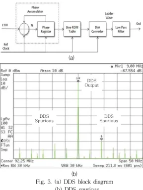
Fig. 3. (a) DDS block diagram (b) DDS spurious
Fig. 3.(a), which shows DDS block diagram, consists of phase accumulator, sine ROM table(Phase to Amplitude Converter), DAC(Digital to Analog Converter) and LPF(Low Pass Filter). DDS spurious arises due to phase truncation of sine ROM table, error in amplitude protons and DAC’s non-linear characteristics.
Phase truncation arises depending on ROM’s number of words, while error in amplitude protons occurs in connection with bits. DDS spurious arises through combination of DDS output frequency harmonic and DDS reference clock frequency harmonic.
Formula (2) is designed to calculate the location of DDS spurious.
× × (2) where : Fspur is DDS spurious position.
Fdds is DDS output frequency.
Fclk is reference clock frequency of DDS.
n, m are harmonic number.
As in Fig. 3 (b), tens of or hundreds of spurious arise from harmonic of DDS output frequency and DDS reference clock frequency harmonic. The spurious directly affects the systems like measurement device. The problem must be resolved.
Recently researchers proposed new technique to eliminate DDS spurious through regular control of digital circuit like DAC by dithering.
This study focuses on proposing ways of projecting and evading the exact location of spurious by analyzing and identifying the cause of spurious without additional change in hardware containing both PLL’s reference spurious and DDS spurious.
IV. In-Band Spurious Occurrences Mechanism
Fig. 4. Spectrum analyzer IF section block diagram Fig. 4 represents block diagram of the IF(Intermediate Frequency) signals processing part of a spectrum analyzer, designed to handle input signals processed as down-covert with 21.4MHz.
RF receiver section of spectrum analyzer consists of 3-stage super-heterodyne and is designed to be converted into low frequency IF frequency to deal with frequency data.
In the past when spectrum analyzer featuring
analog sweep is used, it was hard to recognize RBW(Resolution Bandwidth) between noise level and in-band spurious due to limitation on IF filter technology and phase noise.
In contrast, current spectrum analyzer involving digital IF process requires problem with in-band spurious to be resolved with the advance in RBW technology and reinforced performance of phase noise.
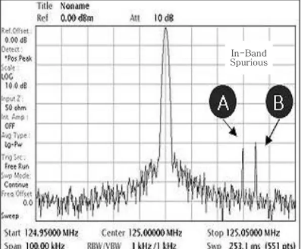
In-band spurious appears through screen of spectrum analyzer as portrayed in Fig. 5 at the place where side band reference spurious converges with 1st local oscillator frequency of frequency synthesizer.
In-Band Spurious
Fig. 5. In-band spurious based on reference spurious
V. In-Band Spurious Analysis and Formulation a Hypothesis
In-band spurious occurs due to spurious from DDS and reference spurious from PLL.
As described above, since the spectrum analyzer consists of hybrid frequency synthesizer. Spurious of PLL and DDS are generates incidental spurious by inter-modulation.
Thus, the study focused on extracting factors potentially causing occurrence of reference spurious, identifying in-band spurious and then creating mathematic modeling for reference spurious that occur through interaction. The factors extracted are described as follows.
Hypothesis 1 : Harmonic combination of 8 diffused frequency on 1st phase locked loop and half frequency from DDS.
Hypothesis 2 : Combination of phase frequency detector reference frequency on 1st phase locked loop, frequency output from DDS and harmonic.
Hypothesis 3 : Harmonic combination of comparison frequency from R-divider and N-divider of phase frequency detector.
By formulating hypothesis1, 2 and 3, our study calculated the exact location of in-band spurious, changed the DDS output frequency and developed ways of evading in-band spurious in advance.
Hypothesis 1 suggests that half frequency of DDS output frequency set N-divider and R-divider at 2 of 2nd phase locked loop considering that comparison frequency is half of DDS output frequency.
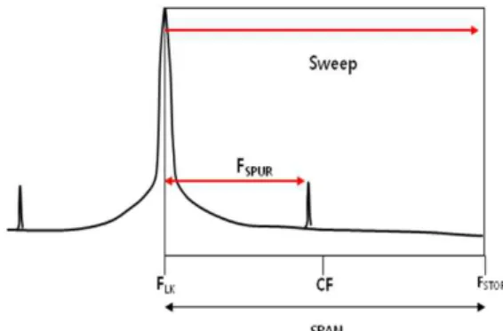
Fig. 6. In-band spurious parameter
Fig. 6 is about where spurious occurs through the screen of spectrum analyzer.
FLK represents initial frequency of span, while Fspur
refers to difference between where span starts and where in-band spurious appears. X is used as the difference of frequency.
When output frequency of frequency synthesizer is in motion, reference spurious comes to move at both sides of output frequency. When movement speed of frequency synthesizer is the same with that of the reference spurious, it may regarded as spurious from fundamental factors. When the movement is faster twice that of output frequency, it may be
regarded as spurious caused by 2nd harmonic.
VI. Mathematical Modeling and Verification of Hypothesis
The study created mathematic modeling based on Fig. 6. formula (3) may represent the mathematic modeling.
± (3) where : FLK is lock frequency.
X is difference of spurious from initial frequency of span.
Fspur is spur related frequency(spur function).
CF is center frequency.
3621.4 is offset frequency of 1st LO.
By changing functions in Fspur regarding hypothesis 1, 2 and 3 in formula (3), the study calculated the location of in-band spurious. The reason 3621.4 is added is that frequency synthesizer output frequency of spectrum analyzer is equal to between 3621.4MHz and 6621.4MHz. This is always larger than center frequency. In other words, offset value is 3621.4MHz. If output range of frequency synthesizer is F1 1000MHz to F2 2000MHz, offset value should be replaced with 1000.
Proof 1 : Harmonic combination of 8 diffused frequency on 1st phase locked loop and half frequency from DDS.
If it is assumed that lock occurs at the center of span frequency synthesizer in spectrum analyzer, spurious function will follow as described in formula(4) in hypothesis 1.
× ±
× (4)
where : Fpllis 1/8 frequency of 1st PLL.
Fdds is DDS output frequency.
n, m are harmonic number.
Fspur1 is hypothesis1 spur function.
In-band spurious occurs in the place where 1st LO converges with reference spurious. Formula 5 is the result of reflecting amount X in motion of 1st LO and amount X in motion of DDS into formula 3 and formula (4).
±
± × ±
× (5) According to formula (5),
If formula (5) is applied in connection with X, formula (6) and (7) will follow. In-band spurious occurs apart from FLK, X1 and X2.
× ×
(6)
× ×
(7)
Proof 2 : Combination of reference frequency of phase frequency detector on 1st phase locked loop and output frequency from DDS.
This shows that harmonic of 8 diffused signals of 1st phase locked loop is compared with the frequency of 2nd phase locked loop.
Under the multiple PLL structure, frequency elements arising from 2nd phase locked loop should be reflected as well as that of 1st phase locked loop.
In case of half elements found in DDS and mixer IF frequency, Fadf, entered as reference frequency in 1st phase locked loop, they are diffused in 1/2 inside PFD of 2nd phase locked loop for comparison so that harmonic can occur.
Spurious function of hypothesis 2. may be described as formula (8) and may be used for formula 3. As a result formula (9) and (10) will follow.
×
×
(8)where : Fadf is mixer IF frequency of 1st PLL Fdds is DDS output frequency
n, m are harmonic number Fspur2 is hypothesis2 spur function
× ×
(9)
× ×
(10)Proof 3 : Harmonic combination of DDS output frequency and comparison frequency by R-divider and N-divider of phase frequency detector on 1st phase locked loop.
Multiple PLL circuit has PLL output frequency acting as reference frequency for different PLL. In this case, harmonic of comparison frequency inside PLL appears, causing another in-band spurious thru the mixture of frequency elements of PLL circuit using the output frequency as reference frequency.
If comparison frequency on PFD of 1st phase locked loop is set as FΦ, frequency multiplier of FΦ will be left alone in Fpll, causing in-band spurious thru inter-modulation with Fdds.
Spurious function of hypothesis3 is described in formula (11). When it applies to formula (3) in connection with X, formula(12) and (13) will follow.
× × (11) where : FΦ is 1st PLL PFD comparison frequency
Fpll is 1/8 frequency of 1st PLL Fdds is DDS output frequency n, m are harmonic number Fspur3 is hypothesis3 spur function
× ×
(12)
×
×
(13)
Ⅶ. In-Band Spurious Evasion Algorithm Verification
In modeling phase, the exact location of in-band spurious is simulated and verified thru measurement.
The proposed formulas contained DDS as common factor, allowing users to easily change frequency only by altering FTW (Frequency Tuning Word).
In other words, all that is needed to change location of in-band spurious is the alteration in DDS frequency.
Fig. 7 show the measurement of 1st LO of frequency synthesizer in spectrum analyzer.
Through this, it may be identified that change in DDS output frequency may lead to the change in location of reference frequency. By changing 1st LO of frequency synthesizer in spectrum analyzer, you can move reference spurious so far away that reference spurious may not appear in span of spectrum analyzer.
(a)
Fig. 7. (a) DDS spurious at 3.3914084GHz(b) (b) Not existing spurious at 3.3914084GHz
Fig. 8 represents characteristics of loop filter of spectrum analyzer, with cutoff-frequency reaching 100KHz. Considering the response curve of loop filter, you can limit the span of the spectrum analyzer to 200KHz for application of proposed algorithm. When span reaches more than 200KHz, cutoff frequency of loop filter will amount to 30KHz.
In such a situation, even when reference spurious occurs, restraint may be applied through the use of loop filter. When the range lies within 30KHz, phase noise characteristically gets worse due to filter’s characteristics. Even when in-band spurious lies within the boundary of bandwidth, it seems non-existent through the screen because it becomes smaller than noise level.
Fig. 8. Response curve of loop filter
Thus, in-band spurious algorithm is applicable only when span reaches less than 200KHz.
System main processor carries out calculation using proposed algorithm to move the in-band spurious and uses calculated value to control 1st
phase locked loop and 2nd phase locked loop through controller. By setting initial frequency at changed reference frequency, in-band spurious may be
Fig. 9. In-Band spurious evasion algorithm moved for evasion.
The algorithm aimed at moving in-band spurious of system main processor is described in Fig. 9, this can be entered by randomly setting reference frequency within the measurable range. Based on randomly established reference frequency, you can enter frequency range (SPAN: 200KHz) that users want to see.
Central processing unit may determine whether spurious exists within the frequency range (SPAN;
200KHz) entered in 2nd phase locked loop. The determination is made through application of formula (6),(7),(9),(10),)(12) and (13).
When in-band spurious is found in span, you can change initial frequency of DDS into the one free of in-band spurious.
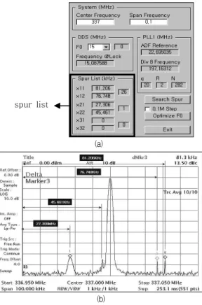
Fig. 10 requires input of center frequency and span along with change in output frequency of DDS so that parameter identical with input condition of spectrum analyzer may be entered. The location of in-band spurious is calculated on condition that
spur list
(a)
(b)
Fig. 10. (a) In-band spurious calculation program (b) In-band spurious measurement
input frequency (337MHz), span(100KHz) and basic output frequency of DDS are 15MHz. In doing so, a total of four Spurious was identified. Fig. 10 (b) shows that four matched spurious is identified as a result of conducting test by allowing input through spectrum analyzer.
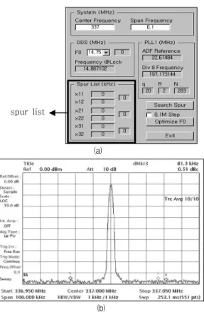
Fig. 11 (b) shows spectrum analyzer after evasion of in-band spurious. This shows that in-band spurious may be evaded by changing output frequency of DDS into 14.75MHz, the closest figure to 15MHz under conditions identical with Fig. 10 (a).
spur list
(a)
Fig. 11. (a) In-band spurious calculation program(b) (b) In-band spurious measurement
Ⅷ. Conclusion
Reference spurious and other harmonic elements occurring to multiple PLL(Multiple Phase Locked Loop) may not eliminated without applying additional filtering or seamless blocking. In addition, PLL IC(Phase locked loop integrated circuits or synthesizer) is compare the internal frequency as a square wave, the harmonic signal is mixed with the output signal. Therefore, it needs a excellent shape factor filter for eliminating of spurious generated by the multiple PLL circuit. More importantly, isolation must be reinforced among electric filters and components. But this does not completely guarantee elimination of in-band spurious though it may be effective in reducing amplitude.
Unlike existing methods (involving change or addition of hardware), the study created mathematic modeling to identify cause of in-band spurious and then verified using MATLAB simulation. After that,
the study embedded the proven formula into CPU to move frequency of DDS so that lock may take place within the area free of spurious.
The proposed algorithm is applicable using frequency scheme of block diagram in Fig. 1, while it may be applicable to other types of DDS driven frequency synthesizer. Thus, the proposed method is expected to contribute to eliminating in-band spurious in system mentioned above as well as in all types of DDS driven frequency synthesizer.
References
[1] Vadim Manassewitsch,"Frequency Synthesizers Theory and Design”
[2] U. Rohde, “Digital PLL Synthesizers: Design and Applications”, Prentice Hall, Upper Saddle River,NJ, 1983.
[3] J. Gorsky-Poiel(ed), “Frequency Synthesis and Application”, IEEE Press 1975.
[4] William F.Egan, "Practical RF System Design"
[ 5] Dean Banerjee, National Semiconductor, " PLL Performance"
[6] J. Noordanus, “Frequency Synthesizers A Survey of Techniques”, IEEE Trans. Comm.
Com-17, #2, April, 1969.
[7] V. S. Reingrdt, “Frequency Synthesizer Basics”, Tutorial for the 1993 IEEE International Frequency Control Symposium.
[8] M. Hu, L. Wang, and X. Tang, “A low spurious and small step frequency synthesizer based on PLL-DDS-PLL architecture,” in Proc.11th IEEE Singapore Int. Conf. Commun. Syst. 2008, pp.
1471–1474.
[9] T.M. Higgins, “Analog output system design for a multifunction synthesizer,” Hewlett-Packard J., vol. 40, no. 1, 1989.
[10] Steve Williams, Tony Caviglia, Cadence Design Systems, "Simulating PLL reference spurs"
[11] Chembiyan Thambidurai, Nagendra Krishnapura, Indian Institute of Technology, "Spur reduction in wideband PLLs by random positioning of charge-pump current pulses"
[12] H. T. Nicholas and H. Samueli, “An Analysis of the Output of Direct Digital Frequency
Synthesizers in the Presence of Finite Word Length Effects,” 42nd Frequency Control Symposium,1987.
[13] V. S. Reingardt, “Direct Digital Synthesizers”, Proceedings of the 17th Annual Precise Time and Time Interval Planning Meeting.
[14] V. S. Reinhardt, “Spur Reduction Techniques in Direct Digital Synthesizers”, 1993 IEEE International Frequency Control Symposium.
[15] F. Bohn, K. Dasgupta, and A. Hajimiri,
“Closed-loop spurious tone reduction for self-healing frequency synthesizers,” in IEEE Radio Freq. Integr. Circuits Symp., Jun. 2011, pp. 1–4.
[16] Zhang Jun-an, Li Guang-jun, Zhang Rui-tao, Li Jiao-xue, Wey Ya-fenng, Yan Bo and Li Ru-zhang,
“ A 2.5GHz Direct Digital Frequency Synthesizer with spurious noise cancellation”, IEICE Electronics Express, Vol.11, No.14, 1-11, July 25 2014.
[17] F.Bohn, K.Dasgupta and A.Hajimiri,
“Closed-loop spurious tone reduction for self-healing frequency synthesizers,” IEEE RFIC Sym. Dig., June 2011.
[18] Alexander Chenakin, “Frequency Synthesis : Current Solutions and New Trends”, Microwave Journal, May 2007.
BIOGRAPHY
Kim Seung-woo (Member) 2001 : BS degree in Electrical Engineering, Kumoh National University.
2003 : MS degree in Electrical Engineering, Pusan National University.
2013 : PhD degree in Electrical Engineering,
Pusan National University.
2003~2015 : Research Engineer, Defense Agency for Technology and Quality
His research interests include audio compression, digital signal process and frequency synthesizer design.
Yoo Woo-sung (Member)
2003 : BS degree in
Electronic Engineering, Kwangwoon University.
2002~2015 : Research Engineer, Lignex1
His research interests include frequency synthesizer design, servo loop design and signal generation instruments.