Effect of substrate temperature on the properties of AZO thin film deposited by using facing targets sputtering system
Yu Sup Jung, Myung Kyu Choi, and Kyung Hwan Kim
††
Department of Electrical Engineering, Gachon University, Seongnam, 461-701
ABSTRACT
Al doped ZnO (AZO) thin film was deposited by using Facing Target Sputtering (FTS) system. This work examined the properties of AZO thin film as a function of the substrate temperature. The sputtering targets were 4 inch diameter disks of AZO (ZnO : Al
2O
3= 98 : 2 wt.% ). The properties of electrical, structural and optical were investigated by 4- point probe, Hall effect measurement, x-ray diffractometer (XRD), field-emitting scanning electron microscopy (FE-SEM), and UV/VIS spectrometer. The lowest resistivity of films was 5.67 × 10
−4Ω.cm and the average optical transmittance of the films was above 85% in the visible range.
Key Words : AZO, Substrate temperature, Facing targets sputtering
1. Introduction
Transparent conductive oxide (TCO) film is oxide material that is highly conductive transparent in visible light and conductive. Indium tin oxide (ITO) has been used for transparent conductive electrodes in many photo- electronic devices such as solar cells and flat panel displays [1-3].
Indium is rare metal that limits many applications.
Impurity-doped ZnO semiconductor materials have attractive characteristics owing to its wide direct band gap (3.37 eV), the abundant raw materials, environmental friendliness, and high radiation resistance. It has the exciton binding energy of 60meV, that is larger than the thermal energy at room temperature [4-6]. Therefore, such proper- ties make them well suited for the realization of many opto- electronic applications. Recent researches exhibited that Group III elements-doped ZnO films have low resistivity and high transmittance in the visible range. Based on many reported investigations of the effect of doping ZnO with impurities, Al seems to be the successful and promising ele- ment due to its advantages. Al is the dopant which resulting in high-quality, low-resistivity AZO thin films [7,8].
Generally sputtered thin films properties are influenced by
substrate temperature, power, and pressure. The growth temperature plays a major role for thin film properties determination, the present study is focused on the influence of substrate temperature on structural, optical and electrical properties of Al doped ZnO films.
2. Experimental
2.1. Facing targets sputtering
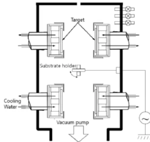
Fig. 1 shows a schematic diagram of facing targets sputtering (FTS) system. The FTS system is an array
†E-mail : [email protected]
Fig. 1. Schematic diagram of FTS system.
target of two sheets that forms high density plasma between the targets. The process is called plasma-free because the substrate is remote from the plasma, which means that bombardment from high energy particles, such as electrons and negative ions, is mini- mized [9].
2.2. Deposition of AZO thin film
In this work, we used the pair of AZO targets. Before film deposition, the glass substrate was cleaned by ultra- sonic cleansing with distilled water and isopropyl alco- hol (IPA) for 30 min. The substrate was then dried in a stream of N
2gas. The chamber was evacuated to 2 × 10
−6Torr before the film deposition. During depo- sition, the pressure was maintained at 1mTorr. The AZO films on the glass substrate were deposited at different substrate temperatures (Room temperature, 100
oC, 150
oC, 200
oC, 250
oC and 300
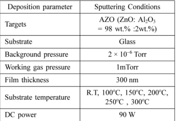
oC). The DC power fixed 90W and the thickness of films fixed 300 nm. Table 1 listed the sputtering conditions.
2.3 Measurements
The electrical properties of the AZO thin films were examined using four-point probe (Chang-min, CMT-1000), and Hall effect measurement (ECOPIA, HMS-3000). The structural properties of the AZO thin films were analyzed by X-ray diffraction (XRD, Rigaku, D/MAX-2200). The surface morphology of AZO thin films was observed by Field Emission Scanning Electron Microscopy (FE-SEM, Hitachi).
The optical transmittance AZO thin films were meas- ured by UV-VIS spectroscopy (HP).
3. Results and Discussions
The AZO thin films exhibited n-type conductivity.
The conductivity of the AZO thin films are domi- nated primarily by electrons generated from Al
3+ions on the substitutional sites of Zn
2+ions and Al intersti- tial atoms [10].
Fig. 2 shows the resistivity, mobility and carrier concentration of AZO thin films as a function of sub- strate temperatures. The minimum value of the resis- tivity of 5.67 × 10
−4Ω..cm was obtained with substrate temperature of 250
oC. Increasing substrate temperature caused the decrease of resistivity. The Hall mobility sharply increased from 11.07 cm
2/V.s to 21.45 cm
2/V.s and the carrier concentration slowly increased from 2.69 × 10
20cm
−3to 4.23 × 10
20cm
−3when substrate temperature increased from R.T to 250
oC. Increased Hall mobility is attributed to improved crystallinity and increased crystallite sizes that weak inter-crystallite boundary scattering and increases carrier lifetime [11].
Deposited AZO thin films showed a c-axis pre- ferred orientation of the (002) (102) plane, as shown in fig.3. Deposited AZO films had a strong (002) XRD peak at value of 34.16
o- 34.24
oat 2θ, and a very weak (102) peak at 44.46
o-44.66
oat 2θ. This suggests that the crystallographic c-axis of the AZO thin films is perpendicular to the substrate, and all AZO thin films had a polycrystalline structure. From fig.3, the preferred orientation for films is increased with sub- Table 1. Sputtering conditions
Deposition parameter Sputtering Conditions
Targets AZO (ZnO: Al
2O
3= 98 wt.% :2wt.%)
Substrate Glass
Background pressure 2 × 10
−6Torr Working gas pressure 1mTorr
Film thickness 300 nm
Substrate temperature R.T, 100
oC, 150
oC, 200
oC, 250
oC , 300
oC
DC power 90 W
Fig. 2. Resistivity, mobility and carrier concentration of
AZO thin films as a function of substrate
temperatures.
strate temperature up to 250
oC. The decrease of the AZO (002) peak for the films deposited at high sub- strate temperatures to the transition region of the Thornton structure zone model [12] where the colum- nar grains change their structure. In addition, a small deviation in (002) peak from the regular position was also found when the substrate was unheated, indicat- ing some residual stress inside the film may exist.
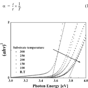
Optical transmittance of the AZO thin films was determined by a UV/Vis. spectrometer within the wavelength from 300 nm to 800 nm. Fig. 4 showed the transmittance of the AZO thin films as a function of substrate temperature. The average optical trans- mittance independent substrate temperature, was over
80% in the visible range (380-770 nm) indicating a high optical transparency. The insert figure showed blue shifts of the optical absorption edge as substrate temperature increased from R.T to 300
oC. The opti- cal absorption coefficient á near the optical absorp- tion edge can be extrapolated by using
(1)
where T is the transmittance of the AZO films near the optical absorption edge and t is the thickness of film.
For AZO thin film, a typical direct band gap semi- conductor, α obeys the following relationship with optical band gap E
g,,(2) where C is a constant, h is Planck's constant, and v is the frequency of the incident photon. Fig. 5 showed the optical bandgap energy of deposited AZO thin film. The E
gvalue can be obtained by extrapolating the linear segments of the curves towards the x-axis.
The E
gvalue increases from 3.54 eV to 3.77 eV from R.T to 300
oC. This means that the substrate tempera- ture affects the optical band gap of the film.
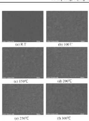
The grain size of the AZO films sharply increased above a substrate temperature of 100
oC, and showed significant temperature sensitivity. The grain size can be estimated using Scherrer’s formula [13].
α ι
t - 1 T ---
×
=
αhv C hv E ( –
g)
12