SPECIAL THEMA
김수현
교수 (영남대학교 신소재공학부)Abstract
Ruthenium (Ru) thin films were grown on thermally-grown SiO2 substrates by atomic layer deposition (ALD) using a sequential supply of four kinds of novel zero-valent Ru precursors, isopropyl-methylbenzene- c y c l o h e x a d i e n e R u ( 0 ) ( I M B C H D R u , C16H22Ru), ethylbenzen-cyclohexadiene Ru(0) (EBCHDRu, C14H18Ru), ethylbenzen-ethyl- cyclohexadiene Ru(0) (EBECHDRu, C16H22Ru), and (ethylbenzene)(1,3-butadiene)Ru(0) (EBBDRu, C12H16Ru) and molecular oxygen (O2) as a reactant at substrate temperatures ranging from 140 to 350℃. It was shown that little incubation cycles were observed for ALD-Ru processes using these new novel zero-valent Ru precursors, indicating of the improved nucleation as compared to the use of typical higher-valent Ru precursors such as cyclopentadienyl-based Ru (II) or β-diketonate Ru (III) metallorganic precursors.
It was also shown that Ru nuclei were formed after very short cycles (only 3 ALD cycles) and the maximum nuclei densities were almost 2 order of magnitude higher than that obtained using higher-valent Ru precursors. The step coverage of ALD-Ru was excellent, around
100% at on a hole-type contact with an ultra- high aspect ratio (~32) and ultra-small trench with an aspect ratio of ~ 4.5 (top-opening diameter: ~ 25 nm). The developed ALD-Ru film was successfully used as a seed layer for Cu electroplating.
1. Introduction
R u t h e n i u m ( R u ) t h i n f i l m s h a v e been investigated for semiconductor microelectronic devices applications, such as a gate for metal-oxide-semiconductor transistor [1], an electrode for the capacitor in dynamic random access memory [2,3] and a seed layer for Cu metallization [4,5] due to its advantages including low resistivity (7.1 μΩ cm for bulk), large work function (4.7 eV), thermal, chemical stability, and feasibility for the dry etch process. Recently, the application of Ru has been extended to nano-scale emerging devices in the form of nano-dots [6,7], nano-tubes [8,9]
and nanocomposites [10], such as nonvolatile memory devices, catalysts and supercapacitors.
For these applications, the Ru films need to be deposited uniformly and fill high aspect ratio (AR) structures with a conformal thickness. In
Highly-conformal Ru Thin Films by Atomic Layer
Deposition Using Novel Zero-valent Ru Metallorganic
Precursors and O 2 for Nano-scale Devices
테 마 기 획 _ 나노 응용기술
addition, a deposition technique with high process controllability that can provide large- area uniformity is essential as the demand for shrinking dimensions is increased. In these respects, atomic layer deposition (ALD) can be a viable solution. Atomic layer deposition consists of four essential steps: 1) precursor exposure, 2) evacuation or purging of the precursors and any byproducts from the chamber, 3) exposure of the reactant species, typically oxidants or reagents, and 4) evacuation or purging of the reactants and byproduct molecules from the chamber (as schematically shown in Fig. 1). Although there are many similarities between ALD and chemical vapor deposition (CVD), the clear and distinctive feature of ALD lies in the self-limitation for precursor adsorption and alternate, sequential exposure of precursors and reactants. This results in the unique characteristics of ALD such as atomic-scale control of the film thickness and composition with excellent step coverage [11,12].
Previously, ALD-Ru thin films have been reported using numerous metalorganic precursors, where a metal valence of the precursors is 2 or 3 [13 ~ 28], and molecular oxygen (O2) as a second reactant. The resulting ALD-Ru films showed excellent properties, such as a low resistivity of 10 ~ 20 μΩ-cm, almost ~ 100 % step coverage in high-aspect ratio structures, and low impurity levels of C and O (below 1 at.
%). Altonen et al. [13] suggested that the subsurface oxygen produced by a molecular O2 pulse reacted with the ligands of the Cp-based Ru precursors provided by the subsequent precursor pulse, producing Ru metal. However, Ru-ALD with these precursors and oxygen reactant shows a
relatively long incubation time with a lower film growth rate at the initial stages of film deposition, which is related to the delayed nucleation of the film material. The use of a β-diketonate Ru precursor of tris(tetramethyl- heptane-dionate) ruthenium(III) [Ru(thd)3, Ru(C11H19O2)3], where the metal valence is 3, showed similar results in terms of Ru nucleation [18]. This results in a deposited film with a rough morphology that is unsuitable for conformal film deposition on high aspect-ratio structures [26]. To reduce the incubation time shown in ALD using a Cp-based Ru precursor, plasma-enhanced atomic layer deposition (PEALD), which employs NH3 plasma as the reactant instead of O2 gas has been studied [15,17,27,28].
Ru films deposited by PEALD showed a negligible incubation cycle [27], and the initial nuclei density is as high as 1012 cm-2, which is ~ 50 times higher than that of ALD using molecular O2 [28]. However, the plasma process usually shows limited applications to film deposition on deep trench or contact structures due to its degraded conformality.
Recent investigations by us showed that
Fig. 1. Schematics showing the growth process of ALD [11].
SPECIAL THEMA
the nucleation of the ALD-Ru process was enhanced considerably by using several zero- valent Ru precursors [29-32]. Such results are summarized and compared to the precursors with higher metal valences in Table 1. Using the zero-valent Ru metallorganic precursors, there were negligible and no incubation cycles on covalent SiO2 and ionic TiN substrates, respectively. Due to the enhanced nucleation, the ALD-Ru films deposited with the zero-valent precursors exhibited an excellent conformality with a smooth surface.
We also evaluated the possibility of ALD-Ru as a seed layer of Cu electroplating for nano- scale devices.
2. Experiments
Ru films were deposited using a travelling-
IMBCHDRu, the second one is ethylbenzen- cyclohexadiene Ru(0) (EBCHDRu, C14H18Ru), third one is ethylbenzen-ethyl-cyclohexadiene Ru(0) (EBECHDRu, C16H22Ru), and fourth one is (ethylbenzene)(1,3-butadiene)Ru(0) (EBBDRu, C12H16Ru). Table 2 shows the molecular structures and vapor pressures of the Ru precursors used in this study. P-type, 4" Si (100) wafers coated with a 100 nm-thick thermally grown SiO2 were used as substrates.
The Ru precursor was vaporized in a bubbler and carried to the process chamber by Ar gas at 50 standard cubic centimeters per minute (sccm). O2 gas was delivered at a flow rate of 50 sccm as the reactant for the Ru precursors.
The deposition temperature was varied from 140 to 350℃. In this study, the basic pulsing condition for the gases, which guaranteed self-limiting film growth, was set based on a previous study as follows; precursor pulse of 5 s, reactant pulse of 0.5 s, and precursor and reactant purge of 10 s.
The thickness of the Ru films was deter mined by cross-sectional view transmission electron microscopy (XTEM, Tecnai F20 equipped with 200 kV accelerating voltage and field emission gun) analysis.
Their resistivities were determined from
Table 2. Information on zero-valent Ru metallorganic precursors.
valence
(cycles) (nm/cycle)
Ru(EtCp)2 2 ~ 210 0.049 17
Ru(Cp)2 2 ~ 250 0.45 13
DER 2 ~ 200 0.2 19
Ru(thd)3 3 ~ 230 0.36 18
IMBCHDRu 0 11 0.086 29
EBCHDRu 0 3 0.1 30
EBECHDRu 0 3 0.041 31
EBBDRu 0 15 0.056 32
Precursors
IMBCHDRu EBCHDRu EBECHDRu EBBDRu
Chemical formula C16H22Ru C14H18Ru C16H22Ru C12H16Ru Vapor pressure
(Torr) 0.2 at 100℃ 0.2 at 100℃ 0.14 at 100℃ 1.2 at 88℃
테 마 기 획 _ 나노 응용기술
the sheet resistances of the Ru films measured using a four-point probe and their thicknesses. The properties of the ALD-Ru films deposited under different deposition conditions were analyzed using various tools.
Impurities in the Ru film, such as oxygen and carbon, were analyzed by secondary ion mass spectroscopy (SIMS, CAMECA IMS- 6f in Korea Basic Science Institute) depth profiling. The SIMS results were calibrated by Rutherford backscattering spectrometry (RBS). The film density was evaluated using X-ray reflectance (XRR, PANalytical X'-pert MRD with Cu-Kα radiation at 1.5 kW). X-ray diffraction (XRD) analysis was performed for phase and crystallinity identification. Plan- view TEM and XTEM were used to examine the microstructures of the Ru films. The step coverage of the ALD-Ru films was evaluated at contacts with the aspect ratio of ~ 4.5 (top opening diameter: ~ 85 nm)
Finally, Cu was electrodeposited on 10-nm thick ALD-Ru film to confirm the feasibility of the film as a seed layer for Cu electroplating.
The Cu plating bath consisted of 0.05 M CuSO4 × 5H2O, 0.05 M (NH4)2HC6H5O7, and NH4OH for pH adjustment. The pH of the bath was 7.0. Cu films were grown directly on the ALD-Ru film by applying a constant cathodic potential of -1.5 V versus a saturated calomel electrode (SCE). Potentiostatic d e p o s i t i o n w a s c a r r i e d o u t u s i n g a potentiostat (IviumStat, Ivium Technologies Inc.). The nucleation and growth mechanism of the Cu film by electrodeposition is critically dependent on the applied cathodic potential.
Normally, as the applied cathodic potential is higher, denser nucleation of Cu deposits is possible in the Cu plating bath used in this study. Therefore, in this study, a relatively
high potential value for Cu reduction on substrates was applied. The morphology of electroplated Cu was examined by cross- sectional view scanning electron microscopy (SEM, Hitachi S-4800).
3. Results and Discussion
Figure 2 shows the thicknesses of ALD-
Fig. 2. The Thickness of ALD-Ru film deposited using IMBCHDRu(0) on SiO2 substrate as a function of the number of reaction cycles [29].
Fig. 3. Plan-view TEM image after (a) 7, (b) 10, (c) 30, and (d) 50 ALD cycles [29].
IMBCHDRu
SPECIAL THEMA
of the number of reaction cycles at ~ 225℃.
The film thickness (characterized by XTEM) increased linearly with increasing number of reaction cycles. The growth rates on the SiO2 substrate determined by linear fitting were 0.086 nm/cycle. The incubation time, which was estimated by the intercept of Fig. 2 with the abscissa at the origin, was ~ 11 cycles.
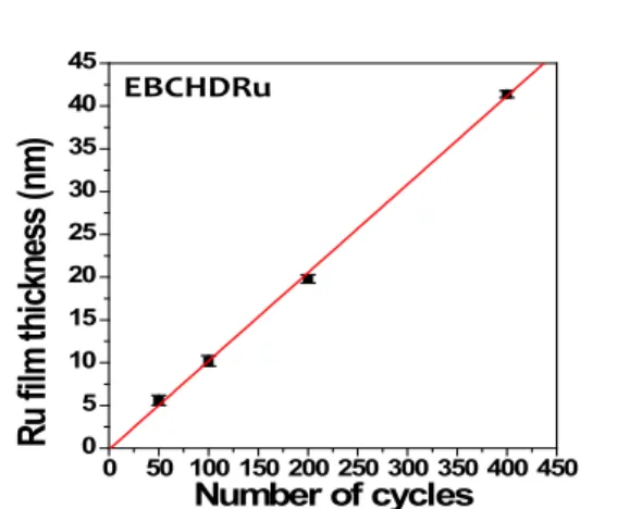
This clearly shows that Ru nucleation was enhanced greatly compared to the results using typical Cp-based Ru(II) metallorganic precursors, beta-diketonate Ru(III) precursor, and DERu(II). Figure 3 shows the morphology of the ALD-Ru films on a thermally grown SiO2 substrate with the number of ALD cycles, as characterized by TEM analysis.
The Ru nuclei were clearly visible after only three ALD cycles (not shown here). As the ALD cycles increased, the nuclei density also increased and the maximum density of the Ru nuclei was 2.1 × 1012 cm-2 on SiO2 at seven ALD cycles. At 10 ALD cycles, coalescence of Ru nuclei occurred at some regions of the SiO2 surface. As the number of ALD cycles was increased to 30, the aggregation and coalescence of Ru nuclei occurs on most of the SiO2 surface. After 50 ALD cycles, a continuous Ru film with a thickness of 3.5 nm was formed.
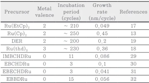
Figure 4 and Fig. 5 shows the growth kinetics and nucleation behavior of ALD- Ru process using EBCHDRu(0) at ~ 225℃.
From Fig. 4, the growth rate, which could be determined by linear fitting, was ~ 0.1 nm/
cycle. The extrapolated line showed that a very short number of incubation cycles, only
~ 2, was needed for the growth of ALD-Ru films, demonstrating a high adsorption of
precursors and a high reactivity of precursors and reactants, leading to the fast nucleation of Ru films on SiO2 surfaces. Figure 5 shows plan-view TEM images of Ru films deposited using EBCHDRu(0) on SiO2 substrate as a function of the number of ALD reaction cycles. After only 3 cycles, nuclei were observed with the density of 9.66 × 1011 cm-2 and the maximum nuclei density of 1.43 ×
Fig. 4. Thicknesses of ALD-Ru films using EBCHDRu(0) deposited on SiO2 at 225 oC as a function of the number of ALD reaction cycles [30].
Fig. 5. Plan-view TEM images of the films deposited on thermally grown SiO2 at 225℃ after (a) 3, (b) 5, (c) 7, and (d) 40 ALD reaction cycles. The basic pulsing condition was used for the film growth [30].
0 50 100 150 200 250 300 350 400 450 0
5 10 15 20 25 30
Ru film thickness (nm)
Number of cycles
테 마 기 획 _ 나노 응용기술
1012 cm-2 was obtained after 5 cycles. After 7 cycles, aggregation and coalescence between nuclei occurred on SiO2 surface. Continuous Ru films were formed only after 40 cycles, which corresponds to the nominal thickness of ~ 4 nm from Fig. 4.
Similar results were also obtained using other zero-valent Ru metalloganic precursor.
Figure 6 shows the plan-view TEM images of ALD-Ru film deposited at 225℃ using EBECHDRu on SiO2 substrate. After only 3 cycles, the Ru nuclei were observed in several sites. Maximum nuclei density was obtained after 7 ALD cycles and is ~ 1.67 × 10¹²/cm2. When the reaction cycles were increased to 30 cycles, coalescence between nuclei was happened. Finally continuous film formed
after only 60 cycles. Figure 7 shows the film thickness as a function of the number of reaction cycles at 225℃ using EBECHDRu on SiO2 substrate. The film thickness increased linearly with an increasing number of reaction cycles at the thickness range of 8 ~ 25 nm. Therefore, the film thickness can be adjusted easily and accurately by the number of reaction cycles. The growth rates on the SiO2 substrates determined by linear fitting were 0.041 nm/cycle. The incubation time, which was estimated by the intercept of Fig. 3 with the abscissa at the origin, was very short,
~ 3 cycles. These results were compared with those from the Ru(EtCp)2 precursor [17].
The ALD-Ru film deposited at 300℃ was not continuous on thermally grown SiO2 even after 500 ALD cycles using the Ru(EtCp)2
precursor and O2 reactant, and the calculated incubation time from the fitting of the thickness with the number of ALD cycles was as high as ~ 210. The maximum density of Ru nuclei was only 5.7 × 10¹⁰ /cm2 on SiO2 at 500 ALD cycles.
Figure 8 shows the thicknesses of ALD-Ru films deposited using EBBDRu(0) on SiO2
Fig. 7. Ru film thickness deposited using EBECHDRu(0) as a precursor on a thermally grown SiO2 substrate as a function of the number of reaction cycles [31].
Fig. 6. TEM analysis of Ru deposited using EBECHDRu(0) as a precursor on a thermally grown SiO2 substrate. Plan- view TEM image after (a) 3, (b) 7, (c) 30, (d) 50, and (e) 60 ALD cycles [31].
30 cycles 50 cycles
3 cycles 7 cycles
60 cycles
(a) (b)
(c) 30 cycles (d) 50 cycles (e)
3 cycles 7 cycles
60 cycles
(a) (b)
(c) (d)30 cycles (e)50 cycles
3 cycles 7 cycles
60 cycles
(a) (b)
(c) 30 cycles (d) 50 cycles (e)
3 cycles 7 cycles
60 cycles
(a) (b)
(c) (d) (e)
30 cycles 50 cycles
3 cycles 7 cycles
60 cycles
(a) (b)
(c) (d) (e)
0 100 200 300 400 500 600 0
5 10 15 20 25
Number of cycle
Ru fi lm th ickn ess ( n m )
EBECHDRuSPECIAL THEMA
with the basic pulsing condition as a function of the number of ALD reaction cycles at the deposition temperature of 225℃. The film thickness depended linearly on the number of ALD reaction cycles. The growth rate, which could be determined by linear fitting, was ~ 0.056 nm/cycle. The extrapolated line showed that a very short number of incubation cycles, only ~ 15, was needed for the growth of ALD-Ru films, demonstrating a high adsorption of precursors and a high reactivity of precursors and reactants, leading to the fast nucleation of Ru films on SiO2
surfaces. Thus, all the results clearly indicated that the use of zero-valent Ru metallorganic precursors significantly improved the nucleation of ALD-Ru processes compared to the use of higher-valent Ru metallorganic precursors. Such results are summarized and compared to the precursors with higher metal valences in Table 1. The issue of nucleation will become more significant with decreasing device sizes and in this respect, a high initial nucleation density is essential to achieve continuity in ultra-thin Ru films.
Due to the enhanced nucleation, the
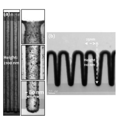
ALD-Ru films deposited with various zero- valent Ru precursors showed an excellent conformality with a smooth surface. As representative results, the step coverages of the ALD-Ru films deposited using IMBCHDRu(0) and EBCHDRu(0) were shown in Fig. 9. Here, they were evaluated at contacts or trenches with different aspect ratios.
Figure 9 (a) shows the step coverage of an ALD-Ru film deposited using IMBCHDRu(0) on a hole-type contact with an ultra-high aspect ratio (~32) and a bottom diameter of 80 nm. Figure 9(b) shows the XTEM of ALD- Ru film deposited using EBCHRu(0) at 225℃
into ultra-small trenches with an aspect ratio of ~ 4.5 (top-opening diameter: ~ 25 nm).
The step coverage was perfect. The excellent step coverage also shows that our Ru films were deposited under ideal ALD growth conditions without partial decomposition of the precursor.
Finally, we investigated Cu electroplating on ALD-Ru films deposited with various zero- valent Ru precursors and the results indicated
Fig. 8. Ru film thickness deposited using EBBDRu(0) as a precursor on a thermally grown SiO2 substrate as a function of the number of reaction cycles [32].
Fig. 9. (a) XTEM image of the contact hole structure with the Ru layer (aspect ratio is 32, top diameter is 89 nm, and bottom diameter is 80 nm) and (b) XTEM image to show the step converges of ALD-Ru films at the trench with the aspect ratio of ~ 4.5 [29,30].
0 100 200 300 400 500 600 0
5 10 15 20 25
Ru film thickness (n
Number of cycles
25nm
Height 110 nm Height:
2100 nm
~ 80 nm (b)
테 마 기 획 _ 나노 응용기술
that the Cu electroplating on all the ALD-Ru films in this study. Here, as representative ones, the results on ALD-Ru film deposited using EBECHDRu(0) were shown in Fig. 10.
The potentiostatic deposition method in the Cu plating bath was used to grow Cu films directly on the surface of the 10-nm-thick ALD-Ru film. The cross-section view SEM image showed that a thin (~ 200 nm) Cu film was deposited directly on the 10-nm thick Ru film prepared by using EBECHDRu(0). This means that the ALD-Ru films developed in this study can be used successfully as a seed layer for Cu interconnects.
4. Summary and Conclusions
We have successfully deposited Ru thin films by thermal ALD using novel zero-valent Ru precursors of isopropyl-methylbenzene- c y c l o h e x a d i e n e Ru ( 0 ) ( I M B C H D Ru , C16H22Ru), ethylbenzen-cyclohexadiene Ru(0) (EBCHDRu, C14H18Ru), ethylbenzen- ethyl-cyclohexadiene Ru(0) (EBECHDRu, C16H22Ru) (ethylbenzene)(1,3-butadiene) Ru(0) (EBBDRu, C12H16Ru) and molecular
oxygen (O2) as a reactant at substrate temperature ranging from 140 to 350℃. This study emphasizes that the use of zero-valent Ru precursors could enhanced the nucleation of ALD-Ru considerably, compared to the utilization of precursors with higher metal valences, such as Cp-based Ru precursors, which have a metal valence of 2, or beta- diketonate Ru precursors, which have a metal valence of 3. This suggests that adsorption of the Ru precursor was increased when a Ru precursor with 0 metal valence was used.
Due to the enhanced nucleation, ALD-Ru deposited with 0 metal valence precursor showed excellent conformality with a smooth film surface at ultra-small contact or trench.
It should be also emphasized that it can also provide other advantage of a lower deposition temperature, which can widen the application fields of ALD-Ru such as flexible electronics using organic or polymer substrates. Finally, as an example of the application of ALD-Ru, it was demonstrated that it could be successfully used as a seed layer for Cu electroplating.
Acknowledgments
This work was supported by National Research Foundation of Korea Grant funded by the Korean Government (2010-0011187).
We thank for Hansol Chemical Inc., Korea for providing the Ru precursors.
References
[1] Y. S. Suh, H. Lazar, B. Chen, J. H. Lee, and V. Misraa, J.
Electrochem. Soc., 152, F138 (2005).
Fig. 10. Cross-sectional view SEM image of a Cu film electrodeposited on the ALD-Ru film prepared using EBECHDRu(0) as a precursor [31].
SPECIAL THEMA
[4] D. Josell, D. Wheeler, C. Witt, and T. P. Moffat, Electrochem.
Solid-State Lett., 6, C143 (2003).
[5] M. W. Lane, C. E. Murray, F. R. McFeely, P. M. Vereecken, and R. Rosenberg, Appl. Phys. Lett., 83, 2330 (2003).
[6] D. B. Farmer and R. G. Gordon, J. Appl. Phys., 101, 124503 (2007)
[7] D. J. Lee, S. S. Yim, K. S. Kim, S. H. Kim, and K. B. Kim, J.
Appl. Phys., 107, 013707 (2010).
[8] W. H. Kim, S. J. Park, J. Y. Son, and H. Kim, Nanotechnology., 19, 045302 (2008).
[9] D. J. Lee, S. S. Yim, K. S. Kim, S. H. Kim, and K. B. Kim, Electrochem. Solid-State Lett., 11, K61 (2008).
[10] J. Biener, T. F. Baumann, Y. Wang, E. J. Nelson, S. O.
Kucheyev, A. V. Hamza, M. Kemell, M. Ritala, and M.
Leskela, Nanotechnology, 18, 055303 (2007).
[11] H. Kim, H.B.R. Lee, and W. J. Maeng, Thin Solid Films, 517, 2563 (2009).
[12] S. M. George, Chem. Rev., 110, 111 (2010).
[13] T. Aaltonen, P. Alën, M. Ritala, and M. Leskelä, Chem. Vap.
Dep., 9, 45 (2003).
[14] S. J. Park, W. H. Kim, W. J. Maeng, Y. S. Tang, C. G. Park, H. Kim, K. N. Lee,S. W. Jung, and W. K. Seong, Thin Solid Films., 516, 7345 (2008).
[15] S. J. Park, W. H. Kim, H.B.R. Lee, W. J. Maeng, and H. Kim, Microelectron. Eng., 85, 39 (2008).
[16] O. K. Kwon, J. H. Kim, H. S. Park, and S. W. Kang, J.
Electrochem. Soc., 151, G109 (2004).
[17] S. S. Yim, D. J. Lee, K. S. Kim, S. H. Kim, T. S. Yoon, and K.
B. Kim, J. Appl. Phys., 103, 113509 (2008).
[18] T. Aaltonen, M. Ritala, K. Arstila, J. Keinonen, and M.
Leskelä, Chem. Vap. Dep., 10, 217 (2004).
[19] S. K. Kim, J. H. Han, G. H. Kim, and C. S. Hwang, Chem.
Mater., 22, 2850 (2010).
[20] W. H. Kim, S. J. Park, J. Y. Son, and H. Kim, Nanotechnology., 19, 045302 (2008).
[21] K. Kukli, M. Kemell, E. Puukilainen, J. Aarik, A. Aidla, T.
Sajavaara, M. Laitinen, M. Tallarida, J. Sundqvist, M. Ritala, and M. Leskelä, J. Electroche. Soc., 158, D158, (2011).
[22] M. Knaut, M. Junige, M Albert, and J. W. Bartha, J. Vac. Sci.
Technol., A 30, 01A151 (2012).
[23] K. Kukli, J. Aarik, A. Aidla, I. Jõgi, T. Arroval, J. Lu, T.
Sajavaara, M. Laitinen, A. A. Kiisler, M. Ritala, M. Leskelä, J. Peck, J. Natwora, J. Gear, R. Sphon, S. Meiere, and D. M.
Thompson, Thin Solid Films., 520, 2756 (2012).
[24] K. Gregorczyk, L. H. Lecordier, J. Gatineau, C. Dussarrat, and G. Rubloff, Chem. Mater., 23, 2650 (2011).
[25] N. Leick, R. O. F. Verkuijlen, L. Lamagna, E. Langereis, S. Rushworth, F. Roozeboom, M.C.M. van de Sanden, and
Belgium, 2008).
[27] O. K. Kwon, S. H. Kwon, H. S. Park, and S. W. Kang, J.
Electrochem. Soc., 151, C753 (2004).
[28] S. S. Yim, D. J. Lee, K. S. Kim, M. S. Lee, S. H. Kim, and K.
B. Kim, Electrochem. Solid-state Lett., 11, K89 (2008).
[29] T. K. Eom, W. Sari, K. J. Choi, W. C. Shin, J. H. Kim, D. J.
Lee, K. B. Kim, H. Sohn, and S. H. Kim, Electrochem. Solid- State Lett., 12, D85 (2009).
[30] S. Yeo, S. H. Choi, J. Y. Park, S. H. Kim, Thin Solid Films, 546, 2 (2013).
[31] T. E. Hong, S. H. Choi, S. Yeo, J. Y. Park, S. H. Kim, T.
Cheon, H. Kim, M. K. Kim, and H. Kim, ECS J. Solid State Sci. Technol., 2, P47 (2013).
[32] S. Yeo, J. Y. Park, S. J. Lee, D. J. Lee, and S. H. Kim, Microelectronic Engineering (Accepted).
![Fig. 1. Schematics showing the growth process of ALD [11].](https://thumb-ap.123doks.com/thumbv2/123dokinfo/4802334.278437/2.807.428.726.122.385/fig-schematics-showing-growth-process-ald.webp)
![Fig. 2. The Thickness of ALD-Ru film deposited using IMBCHDRu(0) on SiO 2 substrate as a function of the number of reaction cycles [29].](https://thumb-ap.123doks.com/thumbv2/123dokinfo/4802334.278437/4.807.431.723.442.703/thickness-deposited-imbchdru-substrate-function-number-reaction-cycles.webp)
![Fig. 10. Cross-sectional view SEM image of a Cu film electrodeposited on the ALD-Ru film prepared using EBECHDRu(0) as a precursor [31].](https://thumb-ap.123doks.com/thumbv2/123dokinfo/4802334.278437/8.807.79.375.134.312/cross-sectional-image-electrodeposited-prepared-using-ebechdru-precursor.webp)
