Regular Paper 486
J. Korean Inst. Electr. Electron. Mater. Eng.Vol. 28, No. 8, pp. 486-489 August 2015
DOI: http://dx.doi.org/10.4313/JKEM.2015.28.8.486 ISSN 1226-7945 (Print), 2288-3258 (Online)
고전압 Field Stop IGBT의 최적화 설계에 관한 연구
안병섭1, 장란향2, 류 용2, 강이구2,a
1 극동대학교 일반대학원 정보통신학과
2 극동대학교 일반대학교 에너지반도체학과
The Optimal Design of High Voltage Field Stop IGBT
Byoung-Sup Ahn
1, Zhang Lanxiang
2, Liu Yong
2, and Ey Goo Kang
2,a1 Department of Information & Telecommunication, Far East University, Eumseong 369-700, Korea
2 Department of Energy Semiconductor Engineering, Far East University, Eumseong 369-700, Korea
(Received July 19, 2015; Accepted July 24, 2015)
Abstract: Power semiconductor device has a very long history among semiconductor, since the invention of
low-pressure bipolar transistor 1947, and so far from small capacity to withstand voltage-current, high-speed and high-frequency characteristics have been developed with high function. In this study, the PWM IC Switch to the main parts used in IGBT (insulated gate bipolar transistor) for the low power loss and high drive capability of the simulator to Synopsys' T-CAD used by the 1,700 V NPT Planar IGBT, 1,700 V FS was a study of the Planar IGBT, the results confirmed that IGBT 1,700 V FS Planar is making about 11 percent less than the first designed NPT Planar IGBT.Keywords: Power device, IGBT, Power switching, Breakdown voltage, Field stop
1. 서 론
70년대에서 성능이 우수한 자동 전력 전자 스위칭 소자 GTR (giant transistor), GTO (gate turn off thyristor), MOSFET (metal oxide semiconductor field effect transistor), IGBT (insulated gate bipolar transistor) 등이 널리 사용되고 있다 [1,2].
파워 반도체 소자는 반도체 중에서도 매우 오랜 역사 를 가지고 있으며, 1947년 바이폴라 트랜지스터의 발
a. Corresponding author; [email protected] Copyright ©2015 KIEEME. All rights reserved.
This is an Open-Access article distributed under the terms of the Creative Commons Attribution Non-Commercial License (http://creativecommons.org/licenses/by-nc/3.0) which permits unrestricted non-commercial use, distribution, and reproduction in any medium, provided the original work is properly cited.
명 이후 저내압, 소용량에서 출발해 현재까지 고내압, 대 전류, 고속 고주파, 그리고 고기능화 특성으로 발전 되어 왔다 [3-5].
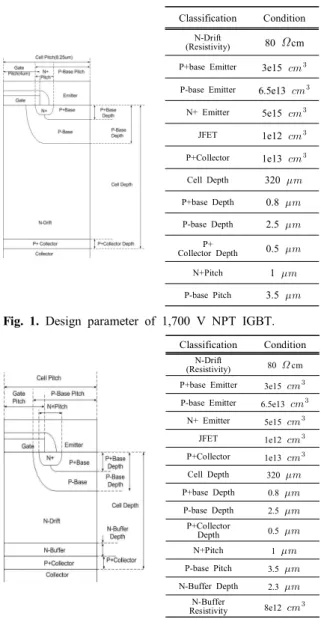
본 연구에서는 모든 산업 분야에 걸쳐서 폭넓게 활 용되고 있는 IGBT 소자(insulated gate bipolar transistor)의 대한 낮은 전력손실과 높은 구동능력을 위하여 소자 및 공정 시뮬레이터인 T-CAD를 이용하 여 1,700 V급 non-punch through IGBT, 1,700 V 급 field stop IGBT에 대하여 연구를 하였다.
2. 실험 방법
2.1 IGBT 구조 및 설계 변수 설정
전기전자재료학회논문지, 제28권 제8호 pp. 486-489, 2015년 8월: 안병섭 등 487
Classification Condition N-Drift
(Resistivity) 80
cm P+base Emitter 3e15 P-base Emitter 6.5e13 N+ Emitter 5e15 JFET 1e12 P+Collector 1e13
Cell Depth 320
P+base Depth 0.8
P-base Depth 2.5
P+
Collector Depth 0.5
N+Pitch 1
P-base Pitch 3.5
Fig. 1. Design parameter of 1,700 V NPT IGBT.
Classification Condition N-Drift
(Resistivity) 80 cm P+base Emitter 3e15 P-base Emitter 6.5e13
N+ Emitter 5e15
JFET 1e12
P+Collector 1e13 Cell Depth 320
P+base Depth 0.8
P-base Depth 2.5
P+Collector
Depth 0.5
N+Pitch 1
P-base Pitch 3.5
N-Buffer Depth 2.3
N-Buffer
Resistivity 8e12