레이저 마이크로 솔더링과 솔더링 인자
황승준·황성빈·정재필† 서울시립대학교 신소재공학과
Laser Micro Soldering and Soldering Factors
Seung Jun Hwang, Sung Vin Hwang, and Jae Pil Jung†
Department of Materials Science and Engineering, University of Seoul, 163, Seoulsiripdae-ro, Dongdaemun-gu, Seoul 02504, Korea (Received August 10, 2020: Corrected September 28, 2020: Accepted September 29, 2020)
Abstract: In this paper, the principles, characteristics and recent studies of the laser micro soldering are reviewed. The factors which influence laser micro welding and soldering are also included. Laser soldering is a non-contact process that transfers energy to solder joint by a precisely controlled laser beam. In recent electronics industry, the demands for laser soldering are increasing due to bonding for complex circuits and local heating in micro-joint. In laser soldering, there are several important factors like laser absorption, laser power, laser scanning speed, and etc, which affect laser solderability. The laser absorption ratio depends on materials, and each material has different absorption or reflectivity for the laser beam, which requires fine adjustment of the laser beam. Laser types and operating conditions are also important factors for laser soldering performance, and these are also reviewed.
Keywords: Laser micro-soldering, Laser types, Laser power, Electronics packaging
1. 서 론
최근 마이크로 전자, micro-LED, flexible display 등의 제조 분야에서, 마이크로 접합의 중요성이 증가하고 있 다.1)마이크로 접합은 전기/전자, 반도체 등 전통적인 전 자분야는 물론이고, 자동차 전장품 등 다양한 분야에 걸 쳐 적용이 확대되고 있다.2)마이크로 접합 중에서도 특 히, 레이저는 열 영향부 최소화라는 강점을 이용하여, 솔 더링 분야에서 기존의 전면 리플로(Reflow) 솔더링 공정 대신, 국부 리플로 기술로서 고집적화 된 전기회로 제작 및 접합부 결함 등을 해결하기 위해 사용되고 있다.3-5) 또 다양한 레이저의 종류와 빔의 형상은 새로운 제품이나 공 정에 적용 가능하여, 솔더링 분야에서 적용이 확대되고 있다.6-8)
레이저 솔더링의 장점으로는, 레이저 빔을 목표 지점에 정확히 조준 가능해 좁은 공간의 솔더링이 가능하며, 비 접촉식 접합 입열량이 적어서 접합 계면에 금속간 화합 물의 생성이 적고, 열응력이 적으며, 솔더의 급속 가열 및 냉각으로 입자가 미세한 조직이 형성되어 연화가 억제되 는 점 등이 있다.9-11) 반면, 레이저 솔더링의 단점으로는
소재마다 레이저 빔의 흡수율 혹은 반사율이 달라서 알 맞은 레이저의 선택과 정교한 레이저 빔의 조절이 요구 된다.4,12)
전자제품의 환경 유해 문제로 인해 환경 친화적인 제조 공정이 각광받고 있고, 이에 따라 유연솔더는 무연 솔더 로 대체되어 왔다. 또, 무연 솔더링 부의 미세 조직과 솔 더링 부에 생성되는 Cu-Sn계 금속간화합물(intermetallic compound, IMC)는 형상과 두께에 따라 솔더부 특성에 영 향을 미친다.[12], [13] 이에 따라, 레이저 솔더링부에 대한 IMC의 영향에 대하여 이해할 필요성이 증가되고 있다.
또한 전기전자 분야에서 다품종 소량생산, 특수 부품 주 문제작이 요구됨에 따라 유연하게 대처할 수 있는 솔더 링 프로세스 개발의 필요성도 증가하고 있다.[14], [15] 본 논 문에서는 최근 LED 등의 국부 솔더링 기술로 관심을 모 으고 있는 레이저 마이크로 솔더링과 레이저 솔더링에 영 향을 미치는 인자들에 대해서 기술하고자 한다.
2. 레이저 마이크로 접합과 출력 파형 레이저 빔 마이크로 접합은 다양한 분야에 사용되고 있
†Corresponding author E-mail: [email protected]
© 2020, The Korean Microelectronics and Packaging Society
This is an Open-Access article distributed under the terms of the Creative Commons Attribution Non-Commercial License(http://creativecommons.org/
licenses/by-nc/3.0) which permits unrestricted non-commercial use, distribution, and reproduction in any medium, provided the original work is properly cited.
특집 : Laser Micro Soldering and Soldering Factors
적으며 용융 및 응고가 60 ms 정도에 일어나고, 그만큼 접합 후 변형이 작다.24)
레이저는 작업시 필요에 따라 빔의 작동 모드를 continuous wave (CW) 모드와 pulsed 모드로 유연하게 선 택할 수 있다.1,2,25) 이러한 작동 모드는 마이크로 접합 혹 은 솔더링 등에서 폭 넓게 사용되며, 반도체, 자동차 산 업에서 듀얼빔 공법의 레이저가 요구되기도 한다. CW 모 드로 접합할 경우, 접합부의 비드 형상이 균일하게 형성
된다.25,26) Pulsed 모드는 시간에 따른 출력을 여러 방식으
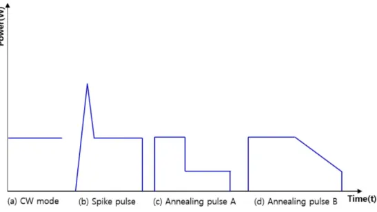
로 조절하여 각 재료 특성에 알맞게 적용시킬 수 있다.25) Fig. 1은 CW 모드와 pulsed 모드의 시간에 따른 여러 가 지 출력 형태 중에서 몇 가지를 나타낸 것이다.
Fig. 1(a)는 일반적인 연속파(continuous wave)를 나타낸 다. 연속파 모드(CW mode)는 보통 짧은 시간(µs) 또는 장 시간(few hours or weeks) 동안 안정적인 레이저를 적용 할 때 사용한다. 반면, 세라믹, Au 혹은 Al과 같이 높은 반사율 때문에 표면의 급속한 증발이 중요한 재료 가공 의 경우에는 Fig. 1(b)와 같이 큰 피크 출력을 주는 spike pulsed 모드를 적용하는 것이 바람직하다.[27] 이 모드는 짧 은 시간 동안 강한 펄스를 가해 열이 레이저 조사 구역 주위에만 집중되어 재료 표면의 급속한 증발을 유발할 수 있는 특징이 있다.27)표면이 급속하게 증발하면 레이저가
있다.31)
3. 레이저 마이크로 솔더링
레이저 솔더링은 전자 패키징 및 상호 연결 등의 표준 제조 공정으로 시작되었다.32,33)이 기술은 각 부품의 온 도 부하, 즉 열 영향을 최소화하고 솔더링부의 위치에 대 한 접근성이 제한될 때 사용하는 것이 특징이다.34,35) 레 이저는 열 영향이 최소화 되기 때문에 다양하고 취약한 IMC 형상(morphology)이 불필요한 곳에 생성되는 것을 방지할 수 있다.36) 또한 이 기술은 플라즈마나 리플로우 솔더링과 비교하여, 처리 시간이 훨씬 짧아서 고속 어셈 블리 라인에 적용할 수 있다.37)특히, 고출력 다이오드 레 이저의 가용성으로 인해, 레이저 빔 솔더링은 합리적인 투자 비용 및 낮은 유지 보수 비용 때문에 시장이 크게 증가하는 추세이다.38)
레이저 솔더링은 플립칩의 경우 100 μm 정도의 작은 솔더 볼을 Si 칩 위에 본 솔더링 전 고정하기 위해 가접 하는데 사용되기도 한다.39) 그러나 좀 더 큰 솔더 볼을 본 격적으로 범핑하는데도 적용된다. Fig. 2(a)은 직경 400 μm의 Sn-3.5Ag 솔더 볼을 Cu/Ni/Au UBM (under bump metallurgy) 위에 위치시킨 후, Nd:YAG 레이저를 사용하
Fig. 1. Various types of laser waves.
여 0.8 J의 입열량으로 레이저 솔더링을 한 것이다. 입열 량이 충분한 Fig. 2(b), (c)와는 다르게 접합이 제대로 되 지 않은 것을 확인할 수 있다. 입열량이 적절한 1.0 J의 경우 솔더 볼이 UBM상에 양호하게 접합되었다. 반면, Fig. 3(c)를 보면, 과도한 레이저 입열량은 접합부에 균열 을 야기할 수 있음을 알 수 있다.40)
Fig. 32)는 마이크로 LED 칩에 사용되는 일반적인 실리 콘 웨이퍼와 투과가 가능한 유리 기판을 이용한 레이저 솔더링을 나타낸 모식도이다. Nd:YAG 레이저가 유리 부 분을 통과하여, 접합 계면의 Si표면에 흡수되면서 접합이 이루어 진다.
레이저 솔더링의 적용 측면에서, QFP (Quad Flat Package) 등의 금속 리드를 솔더 페이스트를 사용하여
레이저로 솔더링하는 것은 가능하다. 또, Ball Grid Array (BGA), Flip Chip (FC) 등의 금속 패드에 솔더 볼 을 레이저로 가열하여 범프를 형성하는 것도 가능하다.
다만, BGA, FC 등의 패키지를 PCB (Printed Circuit Board) 기판 위에 레이저로 가열하여 접합하는 것은 어 려운데, 그 이유는 패키지 아래쪽에 위치한 솔더 볼이 나 범프를 레이저로 직접 조사하여 가열하기 어렵기 때 문이다.
한편, 레이저 보조접합(LAB, Laser Assisted Bonding)은 2차원 빔을 사용하여 레이저와의 간접적 접촉을 통해 솔 더링 한다. 조사된 레이저 빔이 패키지에 흡수되고, 흡수 된 에너지가 솔더링부를 가열하여 솔더링이 이루어진다 . 이 경우 칩이나 패키지 쪽이 솔더보다 먼저 가열되어 온 도가 높아지기 때문에, 전자부품이 열적 손상을 입지 않 도록 주의해야 한다.41)
Fig. 4는 LAB-FU (fluxing underfill) 공정을 보인 것이다.
K.S. Choi 등은 2차원 레이저 빔을 사용하여 반도체 칩이나 패키지를 레이저로 솔더링하는 기술을 개발하
였다.42,43) Fig. 5은 그 결과의 일부로서, 태양전지 모듈을
반도체 레이저로 솔더링한 것이다. Fig. 5(a)는 접합부 단 면 사진을 보인 것으로서, Cu pillar/Sn3.0Ag와 Ni/Au UBM을 접합한 것이다, Fig. 5(b)는 Si 기판에 SAC305 solder paste를 인쇄하여 레이저 솔더링 후 Solar Module 의 변형 정도를 보인 것이다. Fig. 5(a)로부터 접합부 단 면은 양호하게 접합되었음을 알 수 있으며, Fig. 5(b)에서
Fig. 4. LAB-FU (fluxing underfill) process.41)
Fig. 2. Cross sections of solder bumps by laser soldering with different pulse energy (pulse frequency 5 Hz, pulse width 20 ms).40)
Fig. 3. Principle of laser bonding of silicon and glass.2)
레이저 솔더링부 제품이 기존의 리플로 솔더링 제품보다 변형이 작음을 확인할 수 있다.41)
4. 레이저 마이크로 솔더링에 영향을 미치는 요인 우수한 레이저 마이크로 솔더링은 균열이 없고 강도와 신뢰성이 높아야 한다.44) 기공 및 IMC 형성은 레이저 빔 솔더링에서 중요한 관심사이며, 최소화되어야 한다.45)
레이저 솔더링의 품질, 크기 및 특성에 영향을 미치는 여러가지 요인, 즉 변수들이 존재한다.46)예를 들어, 연속 (CW) 모드 레이저 빔과 관련된 변수들로는 레이저 출 력, 빔 크기와 모양, 솔더링부 표면에 대한 빔의 초점면 (focal plane) 위치, 출력 밀도(출력/빔 사이즈), 레이저 빔 의 파장, 포커싱 렌즈의 초점 길이(focal length), 빔의 세 기 분포 등이 있다. 펄스 모드 레이저 빔과 관련된 변수 로는 펄스 에너지, 펄스 반복 속도, 펄스 지속 시간, 평균 레이저 출력(펄스 에너지 × 펄스 반복 속도), 평균 피크 전력 등이 있다. 다른 중요한 요소는 솔더링 속도, 솔더
링 시간, 솔더링 길이 등이다.47)
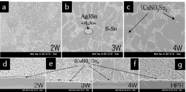
Fig. 647)은 Nd:YAG 레이저를 사용하여 Sn-3.5Ag 솔 더 볼을 Cu/Ni/Au UBM에 솔더링한 경우의 솔더(Fig.
6(a-c)) 및 솔더/UBM 접합계면(Fig. 6(d-g))의 미세조직 을 보인 저자 등의 연구 결과이다. Fig. 6(a-c)에서 레이 저 출력을 2 W에서 4 W로 증가시킴에 따라, β-Sn의 결 정립 크기가 성장됨을 볼 수 있다. Ag3Sn+β-Sn 공정 영 역에서 Ag3Sn 크기도 성장함을 볼 수 있다. Fig. 6(g)는 레이저 출력에 따른 접합 계면과 가열판을 사용한 솔더 링(hot plate reflow, HPR, 250oC, 2s reflow)를 비교한 것 이다. 레이저 솔더링 접합 계면의 금속간화합물인(Cu, Ni)3Sn4는 레이저 출력 증가에 따라 크게 증가함을 볼 수 있다.47)
솔더링부의 크기와 형상 및 미세조직, 경도는 솔더링부 의 신뢰성에 영향을 미치는 중요한 요인이고, 경도가 낮 은 미세한 결정립을 갖는 솔더링부 조직이 바람직하다고 할 수 있다.
Fig. 7은 다양한 레이저 조사 조건에서, 패드 계면과 솔 Fig. 5. Results of LAB for solar module, (a) cross section of Si substrate with Cu pillar/Sn3.0Ag/NiAu UBM, (b) warpage caused by
conventional reflow and LAB.41)
Fig. 6. SEM images of the solder bump microstructure at a heating time of 0.7 s under different laser powers Solder-pad interface.47)
더 사이의 IMC층의 두께를 측정한 저자 등의 보고 결 과47)이다. 먼저, 1 W의 레이저 출력에서는 솔더의 불충 분한 젖음(wetting)으로 인해 신뢰성 있는 IMC 두께를 측 정할 수 없었다. 그러나, 3 W, 4 W 레이저 출력의 경우, IMC의 두께는 가열 시간이 증가함에 따라 빠르게 증가 하였다. 이 때 동일한 입력 에너지 레이저 리플로우에 서, IMC층 두께 성장에는 가열 시간이 레이저 출력 크기 보다 영향력이 큰 인자로 간주된다. 250oC에서 2초간 HPR (hot plate reflow)을 이용하여 형성된 IMC층의 두께 는 그래프에서 기호 ▲로 표시되었다. HPR의 IMC 두께 값은 1.32 μm로 측정되었다. IMC층의 두께는 레이저 리 플로의 경우가 HPR를 이용했을 때에 비하여 대부분 얇 다. 레이저 리플로우에서의 얇은 IMC 두께는 젖음성 감 소와 접합 강도 감소 문제를 완화하고, 계면에서의 과도 한 IMC층 성장으로 인한 전기 저항 증가 문제를 경감시 킨다.47)
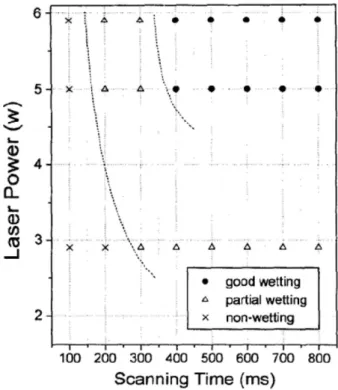
Nd:YAG 레이저를 사용하여 레이저 출력 및 레이저 조사시간(scanning time)에 따라, Sn-3.5%Ag 솔더 페이 스트로 Cu 패드 및 Fe-42%Ni (42 alloy) 리드를 솔더링 한 결과를 저자 등이 보고21)하였다. Fig. 8은 그 결과 로서 젖음성 변화를 나타낸 것이다.젖음성 평가는 솔더 링의 양부를 결정하는 중요한 지표로서 사용된다. Sn- 3.5%Ag 솔더는 5, 5.9 W의 출력하에, 400-500 ms 시간 으로 양호한 젖음성을 나타내었다. 레이저 에너지 측면 에서는 최적 조건은 1-1.25 J/mm으로 나타났다. 반면, 레이저 출력이 5, 5.9 W이고 레이저 조사시간이 100- 300 ms 일 경우에 양호하지 못한 젖음성을 나타낸 것을 알 수 있다.
레이저 솔더링은 다양한 변수에 의해 조절된다. 원하는 형태의 좋은 솔더링을 얻기 위해서 이러한 변수에 대한 이해가 필요하다. 레이저 용융 속도, 즉 솔더링 속도(v) 및 출력(q), 재료의 두께(d) 등에 대한 관계식은 다음과 같이 보고되었다.49,50)
(1)
여기서 k와 j는 상수이고, k는 공정 효율에 영향을 미치는 인자에 의해 결정되며 j는 일반적으로 0.8과 2사이에 있 다. 위 식을 통해 재료의 두께(d)와 출력(q)를 파악하고 적 정 솔더링 속도(v)를 결정하면 양호한 솔더링 결과를 예 측할 수 있을 것이다.
솔더링부에 실제로 흡수되는 입사 레이저 빔의 효율은 재료의 종류와 표면 특성에 의존한다. 레이저 빔에 대한 반사율이 크면 그만큼 효율이 줄어드는데, 반사율을 줄 이기 위한 방법으로는 펄스 형상을 변화시키거나 산소를 혼입시키거나, 반사율이 적은 소재를 코팅하는 방법 등 이 있다.24)
v kq dj ---
=
Fig. 9. Shear strengths under different conditions of laser irradiation.47) Fig. 7. Thicknesses of the IMC layers at the interface with various
laser irradiation conditions(Sn-3.5Ag solder ball on the Cu/Ni/Au UBM).47)
Fig. 8. Effect of laser power and scanning time on the wettability of Sn-3.5%Ag paste on the lead/pad joint. [21]
생하였다.47)
5. 결 론
레이저 공정은 최근 마이크로 전자 분야와 LED 등 소 형 부품 및 형상을 정밀하게 접합하기 위한 다목적 접합 장치로 사용되고 있다. 레이저 공정의 주요 장점인 비접 촉 및 에너지 입력 최소화는 제품의 파손을 줄이고 변형 을 최소화하여, 전자제품의 새로운 디자인과 고집적을 가 능하게 한다. 본 논문에서는 레이저 빔을 이용한 레이저 솔더링과 레이저 솔더링에 영향을 미치는 요소에 대하여 그 연구 동향을 소개하였다. 최근 다양한 파장과 크기가 작은 레이저들을 고성능화 하기 위한 많은 시도들이 진 행되고 있으나, 고성능 파워, 열손실, 냉각기술 등 해결해 야 할 문제들이 다수 존재한다. 또한, 솔더링시 레이저에 의한 급속가열로 솔더가 비산하는 스패터링 등의 문제도 존재한다. 향후 레이저 솔더링에서의 이러한 문제들을 개 선하기 위하여, 금후 더욱 심도 있는 연구와 논의가 필요 하다고 사료된다.
감사의 글
이 연구는 2020년도 산업통상자원부 및 산업기술평가 관리원(KEIT)의 소재부품기술개발사업 연구비 지원에 의한 연구임(‘20010580’, 미니-LED 미세전극 접합을 위 한 도전성 나노소재 기술 개발).
References
1. L. Bosse, A. Schildecker, A. Gillner, and R. Poprawe, “High quality laser beam soldering”, Microsyst. Technol., 7, 215 (2002).
2. A. Gillner, J. Holtkamp, C. Hartmann, A. Olowinsky, J. Gedicke, K. Klages, L. Bosse, and A. Bayer, “Laser applications in microtechnology”, J. Mater. Processing Technology, 167, 494 (2005).
3. A. Bayer, A. Gillner, P. Groche, and R. Erhardt, “Laser-assisted forming of metallic micro-parts”, Proc. 4th International Sym- posium on Laser Precision Microfabrication (SPIE), 5063, 157 (2003).
4. H. Flandorfer, U. Saeed, C. Luef, A. Sabbar, and H. Ipser,
Directed Energy Deposition of Aluminum Powder: Prediction of Geometry and Temperature Evolution”, Materials, 11, 2100 (2018).
8. D. Chattaraj, R. A. Jat, S. C. Parida, R. Agarwal, and S. Dash,
“High temperature enthalpy increments and thermodynamic functions of ZrCo: An experimental and theoretical study”, Thermochim. Acta., 614, 16 (2015).
9. J. W. Xian, S. A. Belyakov, M. Ollivier, K. Nogita, H.
Yasuda, and C. M. Gourlay, “Cu6Sn5 crystal growth mech- anisms during solidification of electronic interconnections”, Acta Mater., 126, 540 (2017).
10. A. Kunwar, H. Ma, H. Ma, B. Guo, Z. Meng, N. Zhao, and M. Huang, “On the thickness of Cu6Sn5 compound at the anode of Cu/liquid Sn/Cu joints undergoing electromigra- tion”, J. Mater. Sci. Mater. El., 27, 7699 (2016).
11. M. Y. Xiong and L. Zhang, “Interface reaction and interme- tallic compound growth behavior of Sn-Ag-Cu lead-free sol- der joints on different substrates in electronic packaging”, J.
Mater. Sci., 54, 1741 (2019).
12. Y. H. Tian and C. Q. Wang, “Microjoining and Nanojoining”, pp.299-326, Woodhead Publishing, Cambridge, UK (2008).
13. H. Nishikawa and N. Iwata, “Formation and growth of inter- metallic compound layers at the interface during laser solder- ing using Sn–Ag Cu solder on a Cu Pad”, J. Mater. Process.
Technol., 215, 6 (2015).
14. H. Nishikawa and N. Iwata, “Improvement of Joint Reliability of Sn-Ag-Cu Solder Bumps on Cu by a Laser Process”, Mater. Trans., 56, 1025 (2015).
15. N. T. Jaya, S. R. A. Idris, and M. Ishak, “The Advances in Joining Technology”, pp.97-107, Springer, Berlin, Germany (2019).
16. T. J. Nabila, S. R. A. Idris, and M. Ishak, “Effect of fiber- lasers parameters on interfacial reaction and wetting angle of two different types of SAC305 solder fabrication on Cu pad”, IOP Conference Series: Materials Science and Engineering, Pahang, Malaysia, 012117 (2019).
17. C. A. Walsh, “Laser welding – Literature Review”, pp.1-21, Materials Science and Metallurgy Department, University of Cambridge, England, July (2002).
18. P. W. Fuerschbach, “Measurement and prediction of energy transfer efficiency in laser beam welding”, Weld. J., 75(1), 24 (1996).
19. J. Bian, L. Zhou, X. Wan, C. Zhu, B. Yang, and Y. A. Huang,
“Laser Transfer, Printing, and Assembly Techniques for Flex- ible Electronics”, Adv. Electron. Mater., 5, 1800900 (2019).
20. K. J. Kim, “Principle and application of laser”, pp.25-53, Daeyoung, Seoul, Korea (1997).
21. J. P. Jung, “A Study on the Solderability of QFP Outer Lead
Using Nd:YAG Laser”, Metals and Materials, 5(3), 317 (1999).
22. A. Olowinsky, K. Klages, and J. Gedicke, “SHADOW® a new welding technique: basics and applications”, Proc. 15th International Symposium on Laser Precision Microfabrication (SPIE), 5662, 291 (2004).
23. MICRO-WELDING, Laser Dynamics, from https://www.laser- dynamics-usa.com/micro-welding
24. M. Calif, “Laser Micro Welding of Conductive Materials”, Industrial Laser Solutions (2011) from https://www.industrial- lasers.com/welding/article/16487468/laser-micro-welding-of- conductive-materials
25. K. A. Jackson, “Current concepts in crystal growth from the melt”, Prog. Solid State Chem., 4, 53 (1967).
26. G. Li, J. Huang, and Y. Wu, “An investigation on microstruc- ture and properties of dissimilar welded Inconel 625 and SUS 304 using high-power CO2 laser”, Int. J. Adv. Manuf. Tech., 76(5-8), 1203 (2015).
27. J. J. Pablo, N. E. Jackson, M. A. Webb, L. Q. Chen, J. E.
Moore, D. Morgan, R. Jacobs, T. Pollock, D. G. Schlom, E.
S. Toberer, J. Analytis, I. Dabo, D. M. DeLongchamp, G. A.
Fiete, G. M. Grason, G. Hautier, Y. Mo, K. Rajan, E. J. Reed, E. Rodriguez, V. Stevanovic, J. Suntivich, K. Thornton, and J. C. Zhao, “New frontiers for the materials genome initia- tive”, NPJ Comput. Mater., 5, 41 (2019).
28. J. Wang, A. Y. Nobakht, J. D. Blanks, D. Shin, S. Lee, A.
Shyam, H. Rezayat, and S. Shin, “Machine learning for ther- mal transport analysis of aluminum alloys with precipitate morphology”, Adv. Theory. Simul., 2, 1800196 (2019).
29. A. Kunwar, S. Shang, P. Råback, Y. Wang, J. Givernaud, J.
Chen, H. Ma, X. Song, and N. Zhao, “Heat and mass transfer effects of laser soldering on growth behavior of interfacial intermetallic compounds in Sn/Cu and Sn-3.5Ag0.5/Cu joints”, Microelectron. Reliab., 80, 55 (2018).
30. “Lasers”, Photonics. Inc. from https://www.coherent.com/assets/
pdf/Lasers___Photonics_Handbook.pdf
31. Vector, “Fundamentals of laser welding” Ee Publishers, (Nov.
19, 2014) from https://www.ee.co.za/article/fundamentals-laser- welding.html
32. S. Lee, J. Peng, D. Shin, and Y. S. Choi, “Data analytics approach for melt-pool geometries in metal additive manu- facturing”, Sci. Technol. Adv. Mater., 20, 972 (2019).
33. S. Wen, K. Chen, W. Li, Y. Zhou, Q. Wei, and Y. Shi, “Selec- tive laser melting of reduced graphene oxide/S136 metal matrix composites with tailored microstructures and mechan- ical properties”, Mater. Des., 175, 107811 (2019).
34. H. Lee, C. H. J. Lim, M. J. Low, N. Tham, V. M. Muruke- shan, and Y. J. Kim, “Lasers in additive manufacturing: A review”, Int. J. Precis. Eng. Manuf.-Green Technol., 4, 307 (2017).
35. T. Hurtony, B. Balogh, and P. Gordon, “Formation and Dis- tribution of Sn-Cu IMC in Lead-Free Soldering Process Induced by Laser Heating”, Micro Nanosystems, 2, 178 (2010).
36. W. K. Choi, S. Y. Jang, J. H. Kim, K. W. Paik, and H. M.
Lee, “Grain morphology of intermetallic compounds at solder joints”, J. Mater. Res., 17, 597 (2002).
37. E. Fereiduni, A. Ghasemi, and M. Elbestawi, “Selective laser melting of hybrid ex-situ/in-situ reinforced titanium matrix composites: Laser/powder interaction, reinforcement forma- tion mechanism, and non-equilibrium microstructural evolu- tions”, Mater. Des., 184, 108185 (2019).
38. T. Yoshida, S. Takeyama, Y. Yamada, and K. Mutoh, “Nano- meter-sized silicon crystallites prepared by excimer laser abla- tion in constant pressure inert gas”, Appl. Phys. Lett., 68(13), 1772 (1996).
39. S, M. Hong, C. S. Kang, and J. P. Jung, “Plasma Reflow Bumping of Sn-3.5 Ag Solder for Flux-Free Flip Chip Pack- age Application”, IEEE Transactions on Advanced Packag- ing, 27(1), 90 (2004).
40. J. O. Kim, “Research on Laser Soldering Process and Solder Bump Characteristics”, in Ph.D. Thesis, pp.11-97, University of Seoul, Seoul, Korea (2009).
41. S. C. Kwang, J. H. Joo, K. S. Jang, G. M. Choi, H. G. Yun, S. H. Moon, and Y. S. Eom, “Laser-Assisted Bonding (LAB), Its Bonding Materials, and Their Applications”, Journal of Welding and Joining, 38(2), 138 (2020).
42. H. Lee, Y. S. Eom, H. C. Bae, K. S. Choi, and J. H. Lee,
“Characterization and Estimation of Solder-on- Pad Process for Fine-Pitch Applications”, Proc. IEEE Transactions on Components, Packaging and Manufacturing Technology (CPMT), 4(10), 1729 (2014).
43. K. S. Choi, Y. S. Eom, S. H. Moon, J. Joo, L. I. Jeong, K.
Lee, J. H. Kim, H. H. Kim, G. S. Yoon, K. H. Lee, C. H. Lee, G. S. Ahn, and M. S. Shim, “Enhanced Performance of Laser- Assisted Bonding with Compression (LABC) Compared with Thermal Compression Bonding (TCB) Technology”, Proc.
69th Electronic Components and Technology Conference (ECTC), Las Vegas, USA, 197, IEEE (2019).
44. S. Katayama, R. Usui, and A. Matsunawa, “Nanomaterials:
Synthesis, Properties and Applications”, pp.467-472, Taylor
& Francis Group, New York, London (1998).
45. M. Pastor, H. Zhao, and T. DebRoy, “Pore formation and composition change during continuous wave Nd: YAG laser welding of aluminum alloys 5182 and 5754”, Trends in Weld- ing Research: Proceedings of the 5th International Confer- ence, Pine Mountain, GA, USA, 455 (1998).
46. Y. Tzeng, “Parametric analysis of the pulsed Nd:YAG laser seam-welding process”, J. Mater., 102, 40 (2000).
47. J. O. Kim, J. P. Jung, J. H. Lee, J. Suh, and H. S. Kang,
“Effects of Laser Parameters on the Characteristics of a Sn- 3.5 wt.%Ag Solder Joint”, Met. Mater. Int., 15(1), 119 (2009).
48. C. S. Song, H. S. Ji, J. H. Kim, J. H. Kim, and H. S. Ahn,
“A Study on the Optimization of IR Laser Flip-chip Bonding Process Using Taguchi Methods”, KWJS, 26(3), 244 (2008).
49. L. H. J. F. Beckmann, D. Ehrlichmann, “Optical systems for high-power laser applications: principles and design aspects”, Opt. Quant. Electron., 27(12), 1407 (1995).
50. J. C. Ion, “Modeling of laser material processing in The Industrial Laser Handbook”, pp.39-47, Springer-Verlog, New York, USA (1992).
• 서울시립대학교 신소재공학과
• 반도체패키징, 접합
• e-mail: [email protected]
• 정 재 필
• 서울시립대학교 신소재공학과
• 분야: 전자패키징, 접합
• e-mail: [email protected]