* E-mail: [email protected] 청정/대체에너지기술
광전기화학 전지를 위한 질소 도핑된 WO 3 박막의 후열처리 효과
안광순*
영남대학교 디스플레이화학공학부 712-749 경북 경산시 대동 214-1
( 2009
년8
월14
일 접수; 2009
년8
월26
일 수정본 접수; 2009
년8
월27
일 채택)
Post-annealing Effect of N-incorporated WO 3 Films for Photoelectrochemical Cells
Kwang-Soon Ahn*
School of Display and Chemical Engineering, Yeungnam University 214-1 Dae-dong, Gyeongsan, Gyeongbuk 712-749, Korea
(Received for review August 14, 2009; Revision received August 26, 2009; Accepted August 27, 2009))
요 약
질소 도핑된 WO3 (WO3:N) 막을 반응성 RF 마그네트론 스퍼터링을 이용하여 상온에서 증착한 다음, 300oC에서부터 500oC의 온도 구간에서 후열처리(post-annealing)하였다. WO3 내 질소 음이온은 O 2p valence state와의 mixing effect에 의해 광학적 밴드갭을 줄임으로써 장파장 영역의 빛을 흡수할 수 있었 다. 더욱이 350oC 이상의 후열처리에 의해 WO3:N의 결정성이 크게 향상됨을 발견하였으며, 동일 온도 에서 열처리된 순수한 WO3 막보다 광전기화학 특성이 휠씬 우수한 셀 성능을 가짐을 알 수 있었다.
주제어: 질소 도핑된 WO3
, 광전기화학적, 후열처리, 결정성, 밴드갭
Abstract : N-incorporated WO
3 (WO3:N) films were synthesized using a reactive RF magnetron sputtering on unheated substrate and then post-annealed at different temperatures from 300 to 500oC in air. The N anion narrowed optical band gap, due to its mixing effect with the O 2p valence states. Furthermore, it was found that the crystallinity of the WO3:N films was significantly improved by the post-annealing at 350oC and higher. As a result, the WO3:N films exhibited much better photoelectrochemical performance, compared with pure WO3 films post-annealed at the same temperature.Keywords: N-incorporated WO
3, Photoelectrochemical, Post-annealing, Crystallinity, Band gap1. Introduction
Photoelectrochemical cell (PEC) systems are promising methods for producing H2 gas in an aqueous solution by solar energy[1-7]. To improve photoelectrochemical properties, the following photoelectrode properties are desirable: (1) a photoelectrode that has high contact area with the electrolyte to increase the interfacial reaction site, (2) a photoelectrode that
has a narrow bandgap to use visible-light energy, and (3) a photoelectrode that has a good crystallinity to reduce the recombination rate of photogenerated electrons and holes. WO3
has been extensively studied in many other technological areas such as electrochromism[8-10], photocatalysis[11], and gas sensors[12], due to their nontoxic, stable, and native n-type semiconductor properties. WO3 is also one of the few inexpensive semiconductors resistant against photocorrosion in
202
an acidic aqueous solution, whose promising utilities in the PEC systems were demonstrated by Miller et al.[13,14] Recently, WO3
electrodes with nanoporous and nanostructured morphologies have been studied to improve photoelectrochemical properties [15-17] pertaining to the above (1). However, energy band gaps, reported from 3.4 to 2.6 eV with variations in crystallinity, only allow the light absorption in the near ultraviolet and blue wavelength region. Thus, the band gap modification would be necessary to use sunlight more efficiently.
Impurity doping in the photoactive metal oxides has been known to shift light absorption to longer wavelengths. Asahi et al.[2] reported that nitrogen anion doping of TiO2 was one of the most effective ways of increasing photo-catalytic activity, because its p-states mix with O 2p-valence band, resulting in the band gap narrowing. In a similar manner, N incorporation into WO3 was recently reported by Paluselli et al.[18], whose band gap could be successfully narrowed down up to 2.2 eV with increasing the concentration of nitrogen. However, despite its effective bandgap narrowing, few results have been, to date, reported relating to the photoelectrochemical responses, due to its inferior crystallinity. Therefore, a good crystallinity is also required for the highly improved photoelectrochemical properties, together with better light absorption in the long wavelength region.
In this article, the N-incorporated WO3 (WO3:N) film was deposited on the substrates, which is not heated, using a reactive RF magnetron sputtering, followed by post-annealing in air at temperatures ranging from 300 to 500oC. Structural, optical, and photoelectrochemical properties of these films were then investigated as a function of increased annealing temperature and compared to those of pure WO3 films without N incorporation. Our data and analyses report that post-annealing of the WO3:N films at temperatures higher than 350oC greatly enhance the crystallinity as well as the band gap narrowing effect of N, compared to the pure WO3 films, resulting in superior photoelectrochemical responses. We also expect that it should prompt developing other technologies such as the electrochromic devices, photocatalysts, and gas sensors.
2. Experimental
WO3:N films were deposited on the non-heated substrates using a reactive RF magnetron sputtering system followed by post-annealing at different temperatures from 300 to 500oC in
air for 5 hr. Conducting transparent FTO (20–23 Ω/sq.)-coated glass was used as the substrate to allow PEC measurements.
The distance between the W metal target and substrate was about 10 cm. The base pressure was below 1×10⁻⁶ torr and the working pressure was 8.8×10⁻³ torr. The chamber was mixed with N2 and O2 flowing at an oxygen gas ratio, O2/(N2+O2) = 3.3%. This low O2 gas flow ratio was required because of its high chemical activity. Prior to sputtering, a pre-sputtering cleaning was performed for 30 min to eliminate possible contaminants from the target. Sputtering was then conducted at a RF power of 150 W. For comparison, a pure WO3 film was deposited at a RF power of 150 W in pure O2 gas environment. All the sputtered samples were controlled to have same film thickness of 1 μm as measured by stylus profilometry.
The characterization of structure and crystallinity were performed by X-ray diffraction (XRD) measurements, using an X-ray diffractometer (XGEN-4000, SCINTAG Inc.), operated with a Cu Kα radiation source at 45 kV and 37 mA. The N concentration in the WO3:N films was evaluated by X-ray photoelectron spectroscopy (XPS). The UV-Vis absorption spectra of the samples were measured by n&k analyzer 1280 (n&k Technology, Inc.) to investigate the optical properties.
Photoelectrochemical measurements were performed in a three-electrode cell with a flat quartz-glass window to facilitate illumination to the photoelectrode surface. The sputter- deposited films were used as the working electrodes. A strip of Pt mesh and an Ag/AgCl electrode were used as the counter and reference electrodes, respectively. A 1-M H2SO4 aqueous solution was used as the electrolyte for the PEC measurements.
The photoelectrochemical response was measured using a fiber optic illuminator (150 W tungsten-halogen lamp) with a UV/IR and combined UV/IR and green filter. The light intensity was measured by a photodiode power meter, in which the total light intensity with the UV/IR filter was fixed at 125 mW/cm2. The photoelectrochemical response data under light on/off illumination were also measured to confirm the photoresponse of the films during the potential sweep (scan rate: 5 mV/s).
3. Results and Discussions
Figures 1(a) and (b) show X-ray diffraction curves for the WO3 and WO3:N films, respectively, annealed at different temperatures. Here, numbers of the samples in Y-axis indicate substrate, as-grown film, and 300, 350, 400, and 500oC-annealed
15 20 2 5 30 35 40 45 50 0
10 00 15 00 20 0 0 25 00
0 1
2345
Intensity (cps)
Samples num bers
2 T heta (2θ )
(a)
15 2 0 2 5 3 0 3 5
40 4 5 5 00
10 00 15 00 20 00 2 50 0
0 1
2345
Intensity (cps)
Samples num bers
2 T heta (2θ )
(b)
Figure 1. X-ray diffraction data for the (a) WO3 and (b) WO3:N films annealed at different temperatures from 300 to 500℃ in air.
15 20 25 30 35 40 45
JCPDS 05-0363
350
oC-annealed WO
3:N
350
oC-annealed WO
3Substrate
In te nsit y (a.u.)
2 Theta ( 2 θ )
Figure 2. The expended intensity scale for the WO3 and WO3:N films annealed at 350℃.
250 300 350 400 450 500
25 30 35 40 45 50 55 60 65
0 2 4 6 8 10
N concentrat ion (at%)
Crystall ite siz e (nm)
Annealing Temperature
(oC
)WO
3WO
3:N
as-grown
Figure 3. Crystallite sizes of the annealed WO3 and WO3: N films and the N concentrations for the WO3: N films as a function of the annealing temperature.
films for (0) to (5), respectively. Both of the unheated as-grown WO3 and WO3:N films exhibited amorphous structures and the crystallinity of the film could be gradually improved with increasing the annealing temperature. Figure 2 showed the expanded intensity scale for substrate and the WO3
and WO3:N annealed at 350oC. It clearly shows that both of the annealed WO3 and WO3:N films display a monoclinic, polycrystalline structure with a main peak at 24.4o corresponding to a (200) plane. Crystallite sizes of the WO3:N films estimated according to the Debye-Sherrer equation were compared to those of the WO3 films, as shown in Figure 3.
The WO3:N films annealed at 350oC or higher exhibited much superior crystallinity than the pure WO3 films, which may be related to the existence of N atoms in the WO3:N film. Figure 3 shows the N concentrations of at% with the annealing temperature for the WO3:N films, as measured by X-ray photoelectron spectroscopy. The as-grown WO3:N film was highly incorporated by the N concentration of about 7.6 at%.
With increasing in the annealing temperature, the N concentration rapidly decreased up to 350oC and then maintained in low N concentration of about 1.5 at% without decrease of the N concentration, indicating that the N atoms were diffused outside the film during the post-annealing and the N solubility limit of about 1.5 at% remained in the film.
From Figures 1(a) and (b), the WO3:N film annealed at 300oC exhibited less crystallinity than the WO3 film at 300oC. It is generally known that excess dopant incorporation can deteriorate the film crystallinity[18-20]. Therefore, inferior crystallinity of the film can be attributed to the existence of still high N incorporation level, as shown in Figure 3, which is in a good agreement with the result reported by Paluselli et al.[18]. On the other hand, greatly enhanced crystallinity of the WO3:N films annealed at 350oC and higher may be due to the moderate amount of N concentration. Similar phenomena have
1.0 1.5 2.0 2.5 3.0 3.5 4.0 0
100 200 300 400 500 600
WO
3films
As-grown 300oC-annealed 350oC-annealed 400oC-annealed 500oC-annealed (α h ν)
1/2(a .u.)
Photon energy(eV) (a)
1.0 1.5 2.0 2.5 3.0 3.5 4.0
0 100 200 300 400 500 600
WO
3:N films
As-grown 300oC-annealed 350oC-annealed 400oC-annealed 500oC-annealed
(α h ν)
1/2(a.u.)
Photon energy(eV) (b)
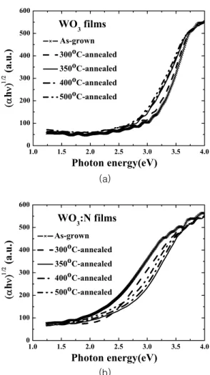
Figure 4. Indirect-transition absorption coefficients for the (a) WO3 and (b) WO3: N films with the different annealing temperatures.
250 300 350 400 450 500
2.0 2.2 2.4 2.6 2.8 3.0 3.2 3.4
WO 3 :N WO 3
O p ti ca l bandgap ( eV)
Annealing temperature
(oC
)as-grown
Figure 5. Estimated optical band gaps of the WO3 and WO3: N films as a function of annealing temperature.
been observed in the Cu-doped, Mn-doped and Bi-doped ZnO films[19,21,22]. They reported that the moderate amount of dopant can reduce activation energy of grain growth or share the oxygen atoms with the metal atoms, leading to the improved crystallinity. Our group previously reported[23] that, when the ZnO is deposited under the mixed sputtering ambient with Ar and N2 at high temperature region, the nitrogen modifies the growth mode and results in the significantly enhanced crystallinity, as compared with the films deposited under pure Ar ambient. More detailed studies of the N effect on the crystallinity are underway.
Figures 4(a) and (b) show indirect-transition absorption coefficient curves for the WO3 and WO3:N films, respectively, with the different annealing temperatures. An indirect optical band gap can be described by the following Eq. 1[18];
(αhν)1/2 = β(hν – Eg) (1)
where hν is photon energy, Eg is an optical bandgap, and β is the edge width. The absorption coefficient α was calculated by the following Eq. 2[18]:
⎟
⎠
⎜ ⎞
⎝
⎛
− −
= R
T d 1 ln 1
α
(2)where d, R, and T are the film thickness, the measured reflectance and transmittance, respectively. The indirect optical band gaps of the films were determined by extrapolating the linear portion of each curve in Figures 4(a) and (b) to (αhν)1/2
= 0, as shown in Figure 5. The amorphous as-grown WO3 film had larger band gap (3.1 eV) than other annealed WO3 films, due to band gap widening via the quantum confinement effect in semiconductor clusters[18,24,25]. The band gap of the pure WO3 films gradually decreased with an increase of the annealing temperature, which is in good agreement with results reported by other groups[24,25]. The as-grown WO3:N film exhibited significantly low band gap less than 2 eV, due to highly incorporated N. However, as increasing the annealing temperature up to 350oC, the band gap of the WO3:N films increased due to the rapidly reduced N concentration, despite superior crystallinity. Thereafter, the bandgap of the WO3:N films gradually decreased from 350 to 500oC, because the crystallinity is enhanced whereas the N concentration is almost constant, as shown in Figures 1(b) and 3. It is worth noting that even the 350oC-annealed WO3:N film exhibited much lower band gap than the 500oC-annealed WO3 film, indicating that this considerable band gap reduction is mainly owing to the band gap narrowing by the N doping, because the 350oC-annealed
400 500 600 700 800 900 1000 0.0
0.1 0.2 0.3 0.4 0.5 0.6 0.7 0.8 0.9 1.0 1.1
For 500
oC-annealed
WO 3 :N
Wavelength (nm)
A b so rb an ce
WO 3
Figure 6. Absorption spectra of the 500℃-annealed WO3 and WO3: N films.
0.0 0.2 0.4 0.6 0.8 1.0 1.2 1.4 1.6 1.8 2.0 2.2 -100
0 100 200 300 400 500 600 700 800
200 300 400 500 600 700 800 900 0
50 100
UV/IR filter
Transmittance (%T)
Wavelength (nm)
Photocurrent ( μ Acm
-2)
Dark currents WO
3:N
Potential (V vs. Ag/AgCl) 500
oC-annealed
WO
3(a)
0.0 0.2 0.4 0.6 0.8 1.0 1.2 1.4 1.6 1.8 2.0 2.2 0
200 400 600 800
Photocu rrent ( μ Acm
-2)
Potential (V vs. Ag/AgCl) 500
oC-annealed WO
3:N
(b)
Figure 7. Photocurrent-voltage curves (1 M H2SO4 aq. sol.
electrolyte and 5 mV/s of scan rate): (a) the 500℃
-annealed WO3 and WO3:N films under illumination with an UV/IR filter, (b) the 500℃-annealed WO3:
N films under light on/off illumination.
WO3:N film has slightly better crystallinity than the 500oC- annealed WO3. Figure 6 shows typical optical- absorption spectra of the WO3 and WO3:N films, respectively, annealed at 500oC. To eliminate the effect from the FTO substrate, the absorbance was calculated by A = 1 − R(film) − T(film) /
T(substrate) [20,26]. The 500
oC-annealed WO3:N film exhibited an absorption tail in the long wavelength region as well as the red-shift of the absorption edge, compared to the WO3 annealed at 500oC. Photoelectrochemical responses of all of WO3:N films in our experiments exhibited n-type photoresponses, which will be discussed later. It indicates that additional n-type donor states such as oxygen vacancy or N-induced new states near the conduction band were simultaneously produced when the N is incorporated. Therefore, the absorption tails in the long wavelength region of the WO3:N films can be attributed to the generation of additional donor states such as the oxygen vacancy or the N-induced new states near the conduction band.Figure 7 shows photocurrent-voltage curves of the WO3 and WO3:N films, respectively, annealed at 500oC under light illumination with an UV/IR filter. Only freshly prepared samples were used for this photoresponse experiment. The 500oC-annealed WO3:N film exhibited anodic photoresponse.
All of the other WO3:N films also showed n-type anodic photoresponses (not shown here), although substitutional N dopants occupied at O sites act as p-type acceptors. Therefore, it indicates that the additional n-type donor states were simultaneously generated when the N is incorporated, which is corresponding well to the absorption spectra in Figure 6. The 500oC-annealed WO3:N film exhibited superior photoelectro- chemical property than the WO3 annealed at 500oC. To confirm whether the photoresponse of the 500oC-annealed WO3:N film
was generated by only absorbed photons without any dark current component, the photoelectrochemical response under light on/off illumination was measured and shown in Figure 7.
The currents under light on and off conditions are the same as the photocurrent under illumination and the dark current, respectively, indicating that the photocurrent of the 500oC- annealed WO3:N film is generated only by absorbed photons under illumination without the contribution of the dark current.
Figure 8 shows the photocurrents measured at 1.6 V as a function of the annealing temperature for the WO3 and WO3:N films. The as-grown and 300oC-annealed WO3 and WO3:N films hardly exhibit the photocurrents. Thereafter, the photocurrent increase with increasing the annealing temperature above 350oC for both of the WO3 and WO3:N films. These trends agree well with the results in Figure 1. The enhanced crystallinity reduces the recombination rate for the
0.6 0.8 1.0 1.2 1.4 1.6 1.8 2.0 0
5 10 15
200 300 400 500 600 700 800 900 0
50 100
UV/IR filter Green filter
Transmittance (%T)
Wavelength (nm)
Dark current of
WO
3:N 500
oC-annealed WO
3500
oC-annealed WO
3:N
Dark current of
WO
3Phot ocu rrent ( μ Ac m
-2)
Potential (V vs. Ag/AgCl)
Figure 9. Photocurrent-voltage curves of the 500℃-annealed WO3 and WO3: N films under light illumination using both the UV/IR and green filters.
250 300 350 400 450 500
0 100 200 300 400 500 600
WO
3WO
3:N
Photocurrent ( μ Acm
-2)
Annealing Temperature (
oC ) At 1.6 V
as-grown
Figure 8. Photocurrents measured at 1.6 V as a function of the annealing temperature for the WO3 and WO3:
N films.
photogenerated electrons and holes, resulting in the improved photoelectrochemical property. Figure 8 also shows that the WO3:N films annealed at 350oC and higher exhibited superior photoresponses than those of the annealed WO3 films. It is attributed to their better light absorption in the longer wavelengths as well as their excellent crystallinity. In order to investigate the photoelectrochemical response in the long wavelength region, a green color filter was used in combination with the UV/IR filter. Figure 9 shows photocurrent- voltage curves of the WO3 and WO3:N films annealed at 500oC under light illumination with the combined filter. The 500oC- annealed WO3 scarcely exhibit photoresponse, compared to the dark current, which corresponds well to the optical absorption result in Figure 6. On the other hand, the WO3:N film annealed at 500oC exhibited the photoelectrochemical response in this long wavelength region. It indicates that, in the case of WO3:N, electron-hole pairs could be generated by light absorption in the longer wavelengths, leading to the photoactive response in the longer wavelength region. It is interesting to note that the photoelectrochemical property of the WO3:N films was not improved in proportion to the dramatically enhanced crystallinity as shown in Figure 1. It indicates that some other recombination centers exist in the WO3:N films. From the analysis of Figure 6 and Figure 7, the WO3:N films most likely contained the additional n-type donor states such as the oxygen vacancy or the N-induced new states near the conduction band, leading to the recombination centers;
the photogenerated electrons and holes are trapped by these additional donor states, limiting photoelectrochemical response.
Nevertheless, the crystalline, N-incorporated WO3 films
exhibited excellent photoelectrochemical responses, owing to the greatly enhanced crystallinity and better light absorption generated from a bandgap narrowing.
4. Conclusions
In summary, the crystalline, N-incorporated WO3 films have been successfully fabricated by the reactive RF magnetron sputtering followed by the post-annealing process in air. The crystallinity of the WO3:N films could be dramatically enhanced by the post-annealing of above 350oC when compared to those of the WO3 films. The N concentration decreased and was then constant in the temperature more than 350oC, whereas the crystallinity was significantly improved as the annealing temperature increased. As a result, the bandgaps of the annealed WO3:N films were narrowed below 2.5 eV due to the N 2p states mixed with the O 2p valence-band states as well as the enhanced crystallinity. However, the N-incorporation into the WO3 created, at a same time, additional n-type donor states such as the oxygen vacancy or the N-induced new states near the conduction band that trap the photogenerated carriers. Nevertheless, the WO3:N films annealed at 350oC and higher exhibited much better photoelectrochemical responses than the annealed WO3 films.
It is due to the greatly enhanced crystallinity and better light absorption in the longer wavelength region. Although more detailed studies for the WO3:N films are required, these results will significantly impact current PEC technologies and have promising implications for the development of electrochromic
devices, photocatalysts, and gas sensors.
Acknowledgement
This research was supported by the Yeungnam University research grant (209-A-054-030) for the PEC application.
References
1. Fujishima, A., and Honda, K., “Electrochemical Photolysis of Water at a Semiconductor Electrode,“ Nature, 238, 37-38 (1972).
2. Asahi, R., Morikawa, T., Ohwaki, T., Aoki, K., and Taga, Y., “Visible-Light Photocatalysis in Nitrogen-Doped Titanium Oxides,” Science, 293, 269-271 (2001).
3. Khaselev, O., and Turner, J. A., “A Monolithic Photovoltaic- Photoelectrochemical Device for Hydrogen Production via Water Splitting,” Science, 280, 425-427 (1998).
4. López, C. M., and Choi, K. S., “Enhancement of Electrochemical and Photoelectrochemical Properties of Fibrous Zn and ZnO Electrodes,” Chem. Commun., 3328-3330 (2005).
5. Ghicov, A., Tsuchiya, H., Macak, J. M., and Schmuki, P.,
“Annealing Effects on the Photoresponse of TiO2
Nanotubes,” Phys. Status. Solidi. A, 203, R28-R30 (2006).
6. Mor, G. K., Shankar, K., Paulose, M., Varghese, O. K., and Grimes, C. A., “Enhanced Photocleavage of Water Using Titania Nanotube Arrays,” Nano Lett., 5, 191-195 (2005).
7. O’Regan, B., and Grätzel, M., “A Low-cost, High- efficiency Solar Cell based on Dye-Sensitized Colloidal TiO2 Films,” Nature, 353, 737-740 (1991).
8. Lee, S.–H., Deshpande, R., Parilla, P. A., Jones, K. M., To, B., Mahan, A. H., and Dillon, A. C., “Crystalline WO3
Nanoparticles for Highly Improved Electrochromic Applications,” Adv. Mater., 18, 763-766 (2006).
9. Lee, S.-H., Cheong, H. M., Tracy, C. E., Mascarenhas, A., Pitts, J. R., Jorgensen, G., and Deb, S. K., “Alternating Current Impedance and Raman Spectroscopic Study on Electrochromic a-WO3 Films,” Appl. Phys. Lett., 76, 3908-3910 (2000).
10. Wang, Y., and Herron, N., “Nanometer-Sized Semiconductor Clusters: Materials Synthesis, Quantum Size Effects, and Photophysical Properties,” J. Chem. Phys., 95, 525-532 (1991).
11. Bosch, H., and Janssen, F., “Formation and Control of Nitrogen Oxides,” Catal. Today, 2, 369-379 (1988).
12. Tao, W. H., and Tsai, C. H., “H2S Sensing Properties of Noble Metal Doped WO3 Thin Film Sensor Fabricated by Micromachining,” Sensor. Actuat. B-Chem., 81, 237-247 (2002).
13. Miller, E. L., Paluselli, D., Marsen, B., and Rocheleau, R.
E., “Development of Reactively Sputtered Metal Oxide Films for Hydrogen-Producing Hybrid Multijunction Photoelectrodes,“ Sol. Energ. Mat. Sol. C., 88, 131-144 (2005).
14. Miller, E. L., Marsen, B., Paluselli, D., and Rocheleau, R.,
“Optimization of Hybrid Photoelectrodes for Solar Water- Splitting,” Electrochem. Solid St., 8, A247-A249 (2005).
15. Santato, C., Ulmann, M., and Augustynski, J.,
“Photoelectrochemical Properties of Nanostructured Tungsten Trioxide Films,” J. Phys. Chem. B, 105, 936-940 (2001).
16. Berger, S., Tsuchiya, H., Ghicov, A., and Schmuki, P.,
“High Photocurrent Conversion Efficiency in Self- Organized Porous WO3,” Appl. Phys. Lett., 88, 203119 (2006).
17. de Tacconi, N. R., Chenthamarakshan, C. R., Yogeeswaran, G., Watcharenwrong, A., de Zoysa, R. S., Basit, N. A., and Rajeshwar, K., “Nanoporous TiO2 and WO3 Films by Anodization of Titanium and Tungsten Substrates:
Influence of Process Variables on Morphology and Photoelectrochemical Response,” J. Phys. Chem. B, 110, 25347-25355 (2006).
18. Paluselli, D., Marsen, B., Miller, E.L., and Rocheleau, R.
E., “Nitrogen Doping of Reactively Sputtered Tungsten Oxide Films,” Electrochem. Solid St., 8, G301-G303 (2005).
19. Wang, X. B., Li, D. M., Zeng, F., and Pan, F.,
“Microstructure and Properties of Cu-Doped ZnO Films Prepared by dc Reactive Magnetron Sputtering,“ J. Phys.
D Appl. Phys., 38, 4104-4108 (2005).
20. Ahn, K.–S., Yan, Y, and Al-Jassim, M., “Band Gap Narrowing of ZnO:N Films by Varying rf Sputtering Power in O2/N2 Mixtures,” J. Vac. Sci. Technol. B 25, L23-L26 (2007).
21. Han, J., Mantas, P. Q., and Senos, A. M. R., “Grain Growth in Mn-Doped ZnO,” J. Eur. Ceram. Soc., 20, 2753-2758 (2000).
22. Senda, T., and Bradt, R. C., “Grain Growth in Sintered
ZnO and ZnO-Bi2O3 Ceramics,“ J. Am. Ceram. Soc., 73, 106-114 (1990).
23. Ahn, K.–S., Shet, S., Deutsch, T., Jiang, C.–S., Yan, Y., Al-Jassim, M., and Turner, J., “Enhanced of Photoelectrochemical Response by Aligned Nanorods in ZnO Thin Films,” J. Power Sources, 176, 387-392 (2008).
24. Granqvist, C. G., Handbook of Inorganic Electrochromic Materials, Elsevier, New York, 1995.
25. Ahn, K.-S., Lee, S.-H., Dillon, A. C., Tracy, C. E., and Pitts, R., “The Effect of Thermal Annealing on Photoelectrochemical Responses of WO3 Thin Films,” J. Appl. Phys. 101, 093524 (2007).
26. Keis, K., Vayssieres, L., Rensmo, H., Lindquist, S. E., and Hagfeldt, A., “Photoelectrochemical Properties of Nano- to Microstructured ZnO Electrodes,” J. Electrochem. Soc.,