Vol. 30, No. 10 (2020)
502
Effect of Low-Temperature Sintering on Electrical Properties and Aging Behavior of ZVMNBCD Varistor Ceramics
Choon-Woo Nahm
†Department of Electrical Engineering, Dongeui University, Busan 47340, Republic of Korea (Received July 23, 2020 : Revised September 14, 2020 : Accepted September 14, 2020)
Abstract
This paper focuses on the electrical properties and stability against DC accelerated aging stress of ZnO-V2O5-MnO2- Nb2O5-Bi2O3-Co3O4-Dy2O3 (ZVMNBCD) varistor ceramics sintered at 850 - 925oC. With the increase of sintering temperature, the average grain size increases from 4.4 to 11.8 mm, and the density of the sintered pellets decreases from 5.53 to 5.40 g/cm3 due to the volatility of V2O5, which has a low melting point. The breakdown field abruptly decreases from 8016 to 1,715 V/cm with the increase of the sintering temperature. The maximum non-ohmic coefficient (59) is obtained when the sample is sintered at 875oC. The samples sintered at below 900oC exhibit a relatively low leakage current, less than 60 mA/cm2. The apparent dielectric constant increases due to the increase of the average grain size with the increase of the sintering temperature.
The change tendency of dissipation factor at 1 kHz according to the sintering temperature coincides with the tendency of the leakage current. In terms of stability, the samples sintered at 900oC exhibit both high non-ohmic coefficient (45) and excellent stability, 0.8% in ΔEB/EB and -0.7 % in Δα/α after application of DC accelerated aging stress (0.85 EB/85oC/24 h).
Key words
Zn-V-based ceramics, sintering, electrical properties, aging behavior, varistors.1. Introduction
Zinc oxide semiconducting ceramics are mainly applied to varistor. This is a smart and attractive electro-ceramic device, which meets a high electrical energy such as electrostatic discharge, transient overvoltage from inductive coil, and lightning. Zinc oxide is an n-type oxide semiconductor due to excess zinc, when compared with oxygen. It exhibits ohmic characteristics in current–voltage relation, whether a single crystalline or a polycrystalline.
However, zinc oxide polycrystalline doped with specified minor additives may exhibit non-ohmic characteristics.
1,2)Zinc oxide varistor ceramics are made by sintering zinc oxide powder doped with minor additives such as Bi
2O
3or Pr
6O
11, CoO, MnO, Cr
2O
3, etc.
1,3)As a result, zinc oxide varistor ceramics are random multi-junction devices, unlike single pn-junction for Si. For this reason, these possess a much higher energy absorption capability than the back-to back Zener diode. Owing to high non-ohmicity and high surge absorption, zinc oxide varistor ceramics are extensively used in the field of transient voltage
protection systems.
4,5)Existing commercial zinc oxide varistor ceramics doped with Bi
2O
3or Pr
6O
11cannot use a silver as an inner- electrode in multilayered components because they are sintered at a temperature as high as 1,000
oC.
1,6)Therefore, they have no choice but to use expensive refractory metal Pd or Pt as an internal electrode. New varistor ceramics based on silver as an internal electrode can be Zn-V system.
7,8)This system has a big advantage, which can be sintered at a relatively low temperature below 900
oC.
9-12)Although many researches for Zn-V system until now, the stability against DC accelerated aging stress for non- ohmic properties is not markedly improved. Some of them exhibited a high stability,
13-15)but not enough to use. We introduce a new varistor ceramic composition ZnO-V
2O
5-MnO
2-Nb
2O
5-Bi
2O
3-Co
3O
4-Dy
2O
3(ZVMNBCD) exhibiting a much higher stability than previously reported.
15)This system exhibited a surprising high stability for varistor properties as well as high non-ohmic properties.
†Corresponding author
E-Mail : [email protected] (C.-W. Nahm, Dongeui Univ.)
©Materials Research Society of Korea, All rights reserved.
This is an Open-Access article distributed under the terms of the Creative Commons Attribution Non-Commercial License (http://creative- commons.org/licenses/by-nc/3.0) which permits unrestricted non-commercial use, distribution, and reproduction in any medium, provided the original work is properly cited.
2. Experimental Procedure 2.1 Specimen Preparation
Varistor samples for test were manufactured by conventional ceramic processing such as weighing, milling and mixing, drying, granulating, pressing, and sintering. Reagent-grade raw materials were prepared in the molar proportion of 96.75 ZnO + 0.5 V
2O
5+ 2.0 MnO
2+ 0.1 Nb
2O
5+ 0.05 Bi
2O
3+ 0.5 Co
3O
4+ 0.1 Dy
2O
3(ZVMNBCD). The weighted powders were ball mixed with acetone into a polypropylene bottle for 24 h. The obtained slurry was dried at 120
oC for 12 h. The dried slurry was blended with acetone and polyvinyl butyral binder (0.8 wt% of powder weight) in a beaker using a magnetic stirring bar. Again the slurry was dried at 120
oC for 24 h. To use the starting powder, the mixture was pulverized and then sieved through a 100-mesh screen. The granulated powder was pressed into disc pellets with a dimension of 10 mm in diameter and 1.5 mm in thickness at a pressure of 1,000 kg/cm
2. The pellets were sintered at 850, 875, 900 and 925
oC in air for 3 h. The sintered pellets were lapped and polished by 1.0 mm thickness using a lapping machine. The final size of the pellets was 8 mm diameter and 1.0 mm thickness.
Both faces of the pellets were painted with conductive silver paste using screen-printing technique, and then
heated at 550
oC for 10 min. The lead wire was soldered on both electrodes and the samples were packaged by dipping it into a thermoplastic resin powder.
2.2 Microstructure Analysis
The sides of the samples were lapped and ground with SiC paper, and then polished with alumina powders. The polished samples were chemically etched at HClO
4–H
2O solution (1:1000, v/v) for 25 s at 25
oC. The microstructure of the surface was examined by a field emission scanning electron microscope (FESEM, Quanta 200, FEI, Brno, Czech). The average grain size (d) was determined by the lineal intercept method such as the following expression, d = 1.56 L/MN, where L is the random line length on the micrograph, M is the magnification of the micrograph, and N is the number of the grain boundaries intercepted by the lines.
16)The crystalline phases were identified by X-ray diffractometer (XRD, X'pert-PRO MPD, Panalytical, Almelo, Netherlands) with CuK
aradiation. The density ( ρ) of the sintered pellets was measured using a density determination kit (238490) attached to balance (AG 245, Mettler Toledo International Inc., Switzerland).
2.3 Electrical and Dielectric Measurement
The electric field-current density (E-J) characteristics were measured using a high voltage source unit (Keithley
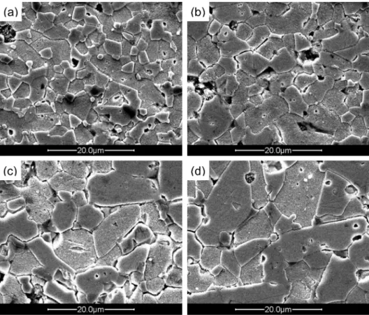
Fig. 1. SEM micrographs of the samples sintered at different temperatures: (a) 850 °C, (b) 875 °C, (c) 900 °C, and (d) 925°C.
237, USA). The breakdown field (E
B) was measured at 1.0 mA/cm
2and the leakage current density (J
L) was measured at 0.8 E
B. The non-ohmic coefficient ( α) was determined through the expression, α = 1/(logE
2–logE
1), where E
1and E
2are the electric fields corresponding to J
1=1.0 mA/cm
2and J
2=10 mA/cm
2, respectively.
The dielectric characteristics, such as the apparent dielectric constant (ε
APP') and dissipation factor (tanδ) were measured in the range of 100 Hz-2 MHz using a RLC meter (QuadTech 7600, USA).
2.4 Aging Stress Measurement
The DC-accelerated aging stress test performed under the stress state of 0.85 E
B/85
oC/24 h. The leakage current was monitored at intervals of 1 min during application of a stress using a high voltage source-measure unit (Keithley 237, USA). After application of a stress, the E- J characteristics were measured at room temperature.
3. Results and Discussion
Fig. 1 shows the SEM micrographs of the samples sintered at different temperatures. It can be seen that the microstructure is featured by homogeneous grains and clear grain boundaries. The behavior of the average grain size (d) and the density ( ρ) of the sintered pellets as a
function of sintering temperature was indicated graphically in Fig. 2. The average grain size of the samples increased from 4.4 to 11.8 mm with the increase of sintering temperature. The sintering temperature had a great effect on the grain size changes, despite small change. Probably, abrupt growth of ZnO grains is attributed to a rich liquid phase related to V
2O
5having a low melting point (690
oC). The sintered density decreased from 5.53 to 5.40 g/cm
3(theoretical density = 5.78 g/cm
3in ZnO) with the increase of sintering temperature. The decrease of the sintered density is assumed to be a result of the volatility of V
2O
5with low melting point (690
oC). The detailed microstructure parameters are summarized in Table 1.
Fig. 3 shows the XRD patterns of the samples sintered at different temperatures. These patterns revealed the presence of Zn
3(VO
4)
2, ZnV
2O
4, and DyVO
4as minor secondary phases, in addition to a major phase of bulk ZnO. The secondary phases were produced by the following chemical reaction.
3ZnO+V
2O
5→ Zn
3(VO
4)
2ZnO+V
2O
5→ ZnV
2O
4+O
2Dy
2O
3+ V
2O
5→ 2DyVO
4The peak of ZnV
2O
4increased gradually when the
Fig. 2. XRD patterns of the samples sintered at different temperatures: (a) 850
°
C, (b) 875°
C, (c) 900°
C, and (d) 925°
C.Table 1. Microstructure, electrical and dielectric parameters of the samples sintered at different temperatures.
Sintering temp. (oC)
d (μm)
ρ (g/cm3)
EB (V/cm)
vgb
(V/gb) α JL
(mA/cm2)
εAPP' (1kHz)
tanδ (1kHz)
850 4.4 5.53 8016 3.5 44 39 330.6 0.211
875 5.7 5.50 4522 2.6 59 36.2 512.7 0.203
900 7.5 5.45 2351 1.7 45 60 985.8 0.206
925 11.8 5.40 1715 2.0 38 100.6 1391.4 0.238
Fig. 3. Average grain size and sintered density as a function of sintering temperature.
sintering temperature decreased. The ZnV
2O
4may have a significant effect on electrical properties and aging characteristics. This means that ZnV
2O
4volatiles with the increase of sintering temperature. By contrast, it can be seen that DyVO
4is considerably stable phase in the small change of sintering temperature.
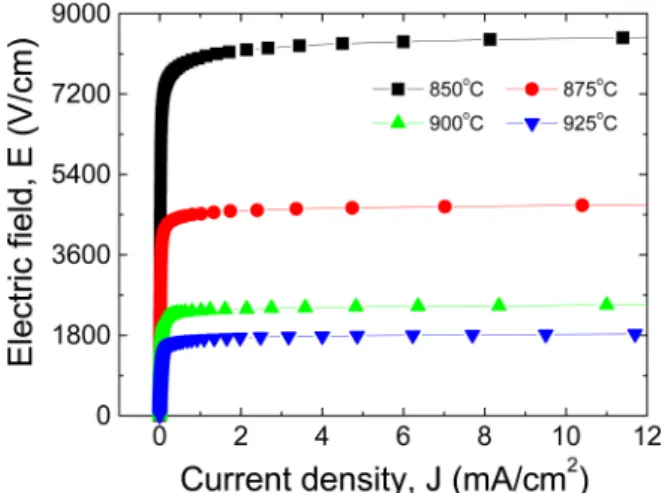
Fig. 4 shows the electric field-current density (E-J) characteristics of the samples sintered at different temperatures. The varistor properties are characterized by the non-ohmic E-J characteristics. In other words, the E- J characteristics show the non-conduction characteristics due to very high resistance below breakdown field and conduction characteristics due to very low resistance above breakdown field. The sharp knee of the curves between the two characteristics will lead to highly non- ohmic properties. However, seemingly, there is no salient difference in the knee of curves. It can be seen from curve shapes that the sintering temperature affects non- ohmic properties. The breakdown field (E
B) abruptly decreased from 8016 to 1715 V/cm with the increase of sintering temperature, despite small change of sintering temperature. The behavior of E
Bin accordance with the sintering temperature can be explained by the grain size:
E
B= v
gb/d, where v
gbis the breakdown voltage per grain boundaries and d is the grain size. E
Bis directly determined by d and v
gbvalue. Among them, d value absolutely affects the E
B. Therefore, the decrease of E
Bwith the increase of sintering temperature is assumed to be result of the increase of the average ZnO grain size.
The non-ohmic coefficient (a) and the leakage current density (J
L) as a function of sintering temperature was indicated graphically in Fig. 5. α value pronouncedly increased from 44 to 59 until the sintering temperature is 875
oC. However, when the sintering temperature exceeded 875
oC, a value decreased to 45 at 900
oC and 38 at 925
o
C. A maximum non-ohmic coefficient (α = 59) was
obtained at 875
oC. The behavior of α according to sintering temperature is related to the variation of the Schottky barrier height formed by the electronic states at the grain boundaries. The sintering temperature will affect the density of interface states at the grain boundary. As a result, this has a sever effect on a. On the other hand, the leakage current density (J
L) decreased from 39 to 36.2 μA/cm
2until the sintering temperature is 875
oC. J
Lis a very low and remarkable value, when compared with ZnO-V
2O
5-based varistors reported until now.
7-15)When the sintering temperature exceeded 875
oC, J
Lincreased to 100.6 mA/cm
2at 925
oC. On the while, this system revealed a relatively low leakage current. The detailed E- J characteristic parameters are summarized in Table 1.
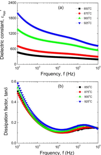
Fig. 6(a) shows the apparent dielectric constant (ε
APP') of the samples sintered at different temperatures. When the frequency increased, ε
APP' decreased due to the decrease of the number of dipole, which can follow to test frequency. ε
APP' increased with the increase of sintering temperature in the range of overall frequency.
This depends on the average grain size and depletion layer width, as the following equation, ε
APP' = ε
g(d/t), where ε
gis the dielectric constant of ZnO (8.5), d is the average grain size, and t is the depletion layer width.
When the sintering temperature increased, the increase of ε
APP' is assumed to be a result of the increase of the average grain size. The dielectric constant (ε
APP') as a function of sintering temperature was indicated graphically in Fig. 7. ε
APP' at 1 kHz linearly increased from 330.6 to 1391.4 at with the increase of sintering temperature. On the other hand, Fig. 6(b) shows the dissipation factor (tanδ) of the samples sintered at different temperatures.
When the frequency increased, tanδ decreased until the vicinity of 10 kHz for all samples and exhibited a dielectric dispersion peak in the vicinity of 200 kHz, and thereafter again decreased. This behavior of tanδ is
Fig. 5. Non-ohmic coefficient and leakage current density as a function of sintering temperature.
Fig. 4. E-J characteristics of the samples sintered at different temperatures.
almost identical for all samples. The dissipation factor (tanδ) as a function of sintering temperature was indicated graphically in Fig. 7. tanδ at 1 kHz value decreased from 0.211 to 0.203 until the sintering temperature is 875
oC.
However, when the sintering temperature exceeded 875
oC, tanδ increased to 0.238 at 925
oC. The behavior of tanδ (1 kHz) according to the sintering temperature exactly coincided with the behavior of leakage current.
The leakage current is one of the factors, which affect tanδ. The detailed dielectric characteristic parameters are summarized in Table 1.
Fig. 8 shows the leakage current (I
L) behavior of the samples during DC accelerated aging stress of 0.85 E
B/ 85
oC/24 h. The behavior of leakage current (I
L) can be divided into greatly 2 groups: the samples sintered at 850
oC, and the samples sintered at 875 - 925
oC. I
Lof the samples sintered at 850
oC abruptly increased and thereafter abruptly decreased within short time. When the stress time increased, I
Lwas almost constant. By contrast, I
Lof the samples sintered at 875 - 925
oC gradually increased and thereafter was almost constant, when the
stress time increased.
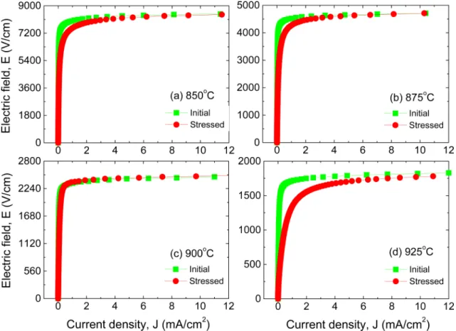
Fig. 9 compares the variation of E-J characteristics after application of a stress with the initial E-J charac- teristics of the samples sintered at different temperatures.
The stability of the samples is secured when the variation of E-J characteristic curves after application of a stress is small, when compared with initial curves. Seemingly, the E-J curves of the samples sintered at 850 and 875
oC have greatly changed in the vicinity of knee. The sample sintered at 925
oC exhibited the largest variation in E-J characteristics after application of a stress. By contrast, the sample sintered at 900
oC exhibited the highest stability without the variation of E-J characteristics after application of a stress. It can be seen that the variation of E-J curves after stress is strongly affected by sintering temperature.
Fig. 10(a) compares E
Bafter application of a stress with initial values of the samples sintered at different temperatures. The decrease rate in E
Bafter application of a stress decreased in the order of 925, 850, 875, and
Fig. 8. Leakage current behavior during DC accelerated aging stress of the samples sintered at different temperatures.Fig. 7. dielectric constant (a) and dissipation factor (b) as a function of sintering temperature.
Fig. 6. Dielectric characteristics of the samples sintered at different temperatures.
900
oC. The samples sintered at 850
oC and 875
oC exhibited the variation rates ( ΔE
B/E
B= -6 %) within 10%
after application of a stress. The sample sintered at 925
°C exhibited the highest variation rate of E
B, reaching ΔE
B/E
B= -21.7 %. By contrast, ΔE
B/E
Bof the sample sintered at 900
oC was only 0.8 %. On the other hand, Fig. 10(b) compares a after application of a stress with initial values of the samples sintered at different tempera-
tures. The samples sintered at 850, 875, and 925
oC exhibited a large decrease of α, reaching Δα/α > -50 % after application of a stress. In particular, the samples sintered at 925
oC exhibited bad non-ohmic properties, in which a is only 8 after application a stress. By contrast, the sample sintered at 900
oC, after application of a stress, exhibited the same a as initial a (45). The variation tendency of a value after stress exhibited the same
Fig. 9. E-J characteristic behavior before and after DC accelerated aging stress of the samples sintered at different temperatures.Fig. 10. Breakdown field (a) and non-ohmic coefficient (b) before and after DC-accelerated aging stress of the samples sintered at different temperatures.
tendency as that of E
Bwith the increase of sintering temperature. On the whole, J
Lvalue after application a stress considerably increased, when compared with E
Band a. The variation rates of the breakdown field ( ΔE
B/ E
B), of the non-ohmic coefficient ( Δα/α), and of the leakage current density ( ΔJ
L/J
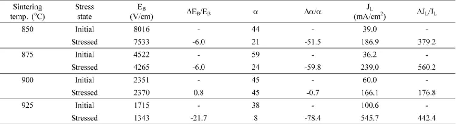
L) after application of a stress for the samples sintered at different temperatures are summarized in Table 2.
4. Conclusions
The microstructure, electrical and dielectric properties, and aging behavior of ZnO-V
2O
5-MnO
2-Nb
2O
5-Bi
2O
3- Co
3O
4-Dy
2O
3(ZVMNBCD) varistor ceramics were in- vestigated at different sintering temperatures of 850 - 925
o
C. The sintered density decreased due to the volatility of V-species related to V
2O
5and the average grain size increased due to the generation of liquid phase with the increase of sintering temperature. The non-ohmic coefficient exhibited a maximum value when the sintering temperature is 875
oC. Further elevated temperatures caused it to decrease. The most important issue in this paper is stability against DC accelerated aging stress. ZVMNBCD varistor ceramics sintered at 900C exhibited an excellent stability as well as high non-ohmic coefficient (45), when compared with Zn-V-based varistor ceramics reported until now. Therefore, it is expected that ZVMNBCD varistor ceramics will be new hope to develop the advanced Zn- V-based varistor ceramics.
References
1. M. Matsuoka, Jpn. J. Appl. Phys., 10, 736 (1971).
2. L. M. Levinson and H. R. Philipp, Am. Ceram. Soc.
Bull., 65, 639 (1986).
3. K. Mukae, K. Tsuda, and I. Nagasawa, Jpn. J. Appl.
Phys., 16, 1361 (1977).
4. D. R. Clarke, J. Am. Ceram. Soc., 82, 458 (1999).
5. T. K. Gupta, J. Am. Ceram. Soc., 73, 1817 (1990).
6. C.-W. Nahm, Mater. Lett., 47, 182 (2001).
7. J.-K. Tsai and T.-B. Wu, J. Appl. Phys., 76, 4817 (1994).
8. J.-K. Tsai and T.-B. Wu, Mater. Lett., 26, 199 (1996).
9. C. T. Kuo, C. S. Chen and I.-N. Lin, J. Am. Ceram. Soc., 81, 2942 (1998).
10. H.-H. Hng and K. M. Knowles, J. Am. Ceram. Soc., 83, 2455 (2000).
11. H.-H. Hng and P. L. Chan, Mater. Chem. Phys., 75, 61 (2002).
12. H.-H. Hng and L. Halim, Mater. Lett., 57, 1411(2003).
13. C.-W. Nahm, J. Mater. Sci.: Mater. Electron., 21, 540 (2010).
14. C.-W. Nahm, J. Mater. Sci.: Mater. Electron., 22, 444 (2011).
15. C.-W. Nahm, J. Mater. Sci.: Mater. Electron., 23, 457 (2012).
16. J. C. Wurst and J. A. Nelson, J. Am. Ceram. Soc., 55,109 (1972).
Author Information
남춘우
동의대학교 전기공학과 교수
Table 2. E-J characteristic parameters before and after DC-accelerated aging stress of the samples sintered at different temperatures.
Sintering temp. (oC)
Stress state
EB
(V/cm) ΔEB/EB α Δα/α JL
(mA/cm2) ΔJL/JL
850 Initial 8016 - 44 - 39.0 -
Stressed 7533 -6.0 21 -51.5 186.9 379.2
875 Initial 4522 - 59 - 36.2 -
Stressed 4265 -6.0 24 -59.8 239.0 560.2
900 Initial 2351 - 45 - 60.0 -
Stressed 2370 0.8 45 -0.7 166.1 176.8
925 Initial 1715 - 38 - 100.6 -
Stressed 1343 -21.7 8 -78.4 545.7 442.4