Vol. 25, No. 1 (2015)
37
Effect of Sintering Temperature on Microstructure, Electrical and Dielectric Properties of (V, Mn, Co, Dy, Bi)-Codoped Zinc Oxide Ceramics
Choon-Woo Nahm
†Semiconductor Ceramics Laboratory, Department of Electrical Engineering, Dongeui University, Busan 614-714, Korea
(Received October 10, 2014 : Received in revised form December 4, 2014 : Accepted December 11, 2014)
Abstract
The effect of sintering temperature on the microstructure, electrical and dielectric properties of (V, Mn, Co, Dy, Bi)- codoped zinc oxide ceramics was investigated in this study. An increase in the sintering temperature increased the average grain size from 4.7 to 10.4µm and decreased the sintered density from 5.47 to 5.37 g/cm3. As the sintering temperature increased, the breakdown field decreased greatly from 6027 to 1659 V/cm. The ceramics sintered at 900oC were characterized by the highest nonlinear coefficient (36.2) and the lowest low leakage current density (36.4µA/cm2). When the sintering temperature increased, the donor concentration of the semiconducting grain increased from 2.49× 10¹⁷ to 6.16× 10¹⁷/cm3, and the density of interface state increased from 1.34× 10¹² to 1.99× 10¹²/cm2. The dielectric constant increased greatly from 412.3 to 1234.8 with increasing sintering temperature.Key words
ZnO-V2O5-based ceramics, sintering, electrical and dielectric properties, varistors.1. Introduction
Zinc oxide is a nonstoichiometric compound semicon- ductor of n-type as containing excess zinc ion, when compared with oxygen ion.
1)Pure zinc oxide sintered exhibits ohmic properties, which are obeyed by the relations V = IR, where R is a function of V, and for which R does not vary as the magnitude of V increases.
However, sintered zinc oxide doped with specified impurities such bismuth and praseodymium exhibits non- ohmic properties, in which R decreases as the magnitude of V increases. This is called varistor effect.
2)Zinc oxide varistor is fabricated by sintering ZnO body doped with minor additives such as Bi
2O
3(or Pr
6O
11), CoO, MnO, Cr
2O
3, etc. Sintering at appropriate tem- perature yields a distinctive microstructure with a multi- junction.
3,4)Zinc oxide varistor exhibits symmetric non- ohmic V-I characteristics similar to back-to-back Zener diode. Zener diode has a single pn junction, a high nonlinearity, and fast response time. By contrast, zinc oxide varistor possesses a very high energy handling capability. For this reason, zinc oxide varistor is widely used as surge protection devices in the electrical and
electronic circuit systems.
3-6)ZnO-Bi
2O
3- or ZnO-Pr
6O
11-based multilayered varistor ceramics require a high sintering temperature exceeding 1000
oC.
2,7,8)Thus, they should be co-fired with ex- pensive refractory metals(Pt, Pd) with high melting temperature as an inner-electrode. Therefore, new varistor ceramics in order to use high conductive silver as an inner-electrode are required. One candidate is ZnO-V
2O
5system.
9,10)This system can be sintered at the vicinity of about 900
oC. ZnO-V
2O
5system doped with MnO
2or Mn
3O
4was recognized as promising varistor ceramics, as exhibiting a good non-ohmic coefficient.
11-14)ZnO-V
2O
5-based varistor ceramics can be interestingly studied in terms of the effect of ceramic composition and sintering process, on microstructure, electrical and die- lectric properties, electrical stability against various stresses, etc. However, on the whole, ZnO-V
2O
5-based varistor ceramics revealed a high leakage current and a low stability, despite high non-ohmic properties.
15-21)At present, ZnO-V
2O
5-based varistor ceramics have a lot of problems to apply to multilayered varistors. Therefore, it is necessary to improve characteristic parameters of ZnO- V
2O
5-based varistor ceramics though diverse experiments.
†Corresponding author
E-Mail : [email protected] (C.-W. Nahm, Dongeui Univ.)
©Materials Research Society of Korea, All rights reserved.
This is an Open-Access article distributed under the terms of the Creative Commons Attribution Non-Commercial License (http://creative- commons.org/licenses/by-nc/3.0) which permits unrestricted non-commercial use, distribution, and reproduction in any medium, provided the original work is properly cited.
38 Choon-Woo Nahm
In this work, the effect of sintering temperature on microstructure, electrical and dielectric properties of (V, Mn, Co, Dy, Bi)-codoped zinc oxide ceramics was systematically investigated and some new results were attained in terms of leakage current.
2. Experimental procedure
The composition recipe of semiconducting varistor was used in the proportion of 96.8 mol% ZnO, 0.5 mol% V
2O
5, 2.0 mol% MnO
2, 0.5 mol% Co
3O
4, 0.1 mol% Dy
2O
3, and 0.1 mol% Bi
2O
3as reagent-grade raw materials. The blended slurry was dried at 120
oC for 12 h. The dried slurry was blended with acetone and polyvinyl butyral binder(0.8 wt% based on powder weight) in a beaker using a magnetic stirring bar. After drying, the blend was granulated by sieving through a 100-mesh screen, to produce starting powder. The sieved powder was pressed into disk-shaped pellets of 10 mm in diameter and 1.5 mm in thickness at a pressure of 100 MPa. The pellets were set on MgO plate into alumina sagger, sintered at different temperatures(875, 900, 925, and 950
oC) in air for 3 h, and furnace-cooled to room temperature. The heating and cooling rates were 4
oC/min. The final pellets were about 8 mm in diameter and 1.0 mm in thickness.
Conductive silver paste was coated on both faces of the pellets by screen-printing techniques, and the electrodes were formed by heating it at 550
oC for 10 min. The electrodes were 5 mm in diameter. Finally, the lead wire was soldered to both electrodes, the samples were packaged by dipping them into a thermoplastic resin powder.
Either side of the samples was lapped and ground with SiC paper, and then polished with 0.3 μm-Al
2O
3powder to a mirror-like surface. The polished samples were chemically etched with HClO
4-H
2O solution(1:1000, v/v) for 25s at 25
oC. The surface microstructure was examined by a field emission scanning electron micro- scope(FESEM, Quanta 200, FEI, Brno, Czech). The average grain size (d) was determined through the lineal intercept method using the expression, d = 1.56 L/MN, where L is the random line length on the micrograph, M is the magnification of the micrograph, and N is the number of the grain boundaries intercepted by the lines.
22)The crystalline phases were identified by using X-ray diffractometer(XRD, X’pert-PRO MPD, Panalytical, Almelo, the Netherlands) with CuK
αradiation. The densities ( ρ) of sintered pellet were measured by using a density determination kit(238490) attached to balance (AG 245, Mettler Toledo International Inc., Greifensee, Switzerland).
The electric field-current density(E-J) characteristics were measured by using a V-I source(Keithley 237,
Keithley Instruments Inc., Cleveland, OH, USA). The breakdown field(E
1 mA/cm2) was measured at 1.0 mA/cm
2, and the leakage current density(J
L) was measured at 0.8 E
1 mA/cm2. The nonlinear coefficient( α) is defined by the empirical law, J = C·E
α, where J is the current density, E is the applied electric field, and C is a constant. α was calculated through the expression,
1)α = (logJ
2− logJ
1) / (logE
2− logE
1), where J
1= 1.0 mA/cm
2, J
2= 10 mA/cm
2, and E
1and E
2are the electric fields corresponding to J
1and J
2, respectively.
The capacitance-voltage(C-V) characteristics of the samples were measured at 1 kHz, using an RLC meter (QuadTech 7600, USA) and an electrometer(Keithley 617, USA). The donor density(N
d) and the barrier height ( Φ
b) were determined through the expression,
23)(1/C
b− 1/2C
bo)
2= 2( Φ
b+ V
gb)/q εN
d, where C
bis the capacitance per unit area of a grain boundary, C
bois the value of C
bwhen V
gb= 0, V
gbis the applied voltage per grain boundary, q is the electronic charge, ε is the permittivity of ZnO( ε = 8.5ε
o). The density of interface states(N
t) at the grain boundary was determined through the equation,
23)N
t= (2 εN
dΦ
b/q)
1/2.
The dielectric characteristics, such as the apparent dielectric constant( ε
APP') and dissipation factor(tanδ) of the samples were measured in the range of 100 Hz-2 MHz using an RLC meter(QuadTech 7600, Marlborough, MA, USA).
3. Results and Discussion
Fig. 1 shows the SEM micrographs of the samples sintered at various temperatures. Outwardly, the micro- structure is not uniform in shape of grain, when compared with zinc oxide doped with bismuth or praseodymium. Changing tendency of the average grain size (d) and the density ( ρ) of the sintered pellets as a function of sintering temperature is indicated graphically in Fig. 2. The average grain size (d) increased in the order of 4.7, 5.8, 7.2, and 10.4 μm when the sintering temperature increased. This is attributed to a strong deriving force for grain growth with the sintering temperature. The density ( ρ) of the sintered pellets decreased slightly in the order of 5.47, 5.44, 5.39, and 5.37 g/cm
3when the sintering temperature increased. The decrease of density ( ρ) with increasing sintering tem- perature is attributed to the volatility of the V-species for V
2O
5with low melting point.
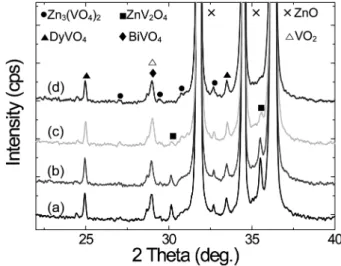
Fig. 3 shows the XRD patterns of the samples sintered
at various temperatures. This system showed many minor
phases such as Zn
3(VO
4)
2, ZnV
2O
4, DyVO
4, BiVO
4, and
VO
2. It seems that V
2O
5additive easily reacts with other
ingredients as well as has low melting point. Among
minor phases, the ZnV
2O
4was found to be greatly
affected by sintering temperature. Particular change of phase is that the peak of ZnV
2O
4(2 θ = 30.0933
o, 35.4420
o) decreases gradually with increasing sintering temperature and finally the peak of ZnV
2O
4was not detected at 950
oC.
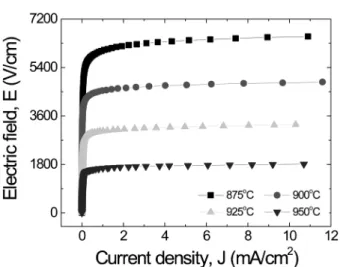
Fig. 4 shows the E-J characteristics of the samples sintered at various temperatures. The varistor’s conduction characteristics are featured by ON/OFF state of current at
threshold voltage. OFF state leads to very high im- pedance at below threshold voltage, and ON state leads to very low impedance at above threshold voltage. All the samples exhibited an equivalent gap between curves with increment by 25
oC in the sintering temperature.
Outwardly, it can be seen that the sintering temperatures
Fig. 1. SEM micrographs of the samples sintered at various temperatures: (a) 875oC, (b) 900oC, (c) 925oC, and (d) 950oC.Fig. 2. Average grain size and sintered density as a function of sintering temperature.
Fig. 3. XRD patterns of the samples sintered at various tempera- tures: (a) 875oC, (b) 900oC, (c) 925oC, and (d) 950oC.
40 Choon-Woo Nahm
has a noticeable effect on the breakdown field of the E-J characteristics. The breakdown field(E
1 mA/cm2) decreased linearly in the order of 6027, 4538, 3041, and 1659 V/cm with increasing sintering temperature. This coincides with the gap size between curves with increasing sintering temperature. E
1 mA/cm2is measured through the expression, E
1 mA/cm2= V
1 mA/cm2/D = (v
b·n)/D = v
b/d, where V
1 mA/cm2is breakdown voltage, D is the thickness of the sample, and n is the number of grain boundaries.
2)E
1 mA/cm2is pre- dominantly controlled by the grain size (d) and slightly depends on the breakdown voltage per grain boundaries (v
b). As a result, the behavior of breakdown field(E
1 mA/cm2
) is directly related to the number of grain boundaries or the average grain size. v
bdecreased in the range of 2.8 to 1.7 V/gb.
Changing tendency of nonlinear coefficient ( α) and leakage current density(J
L) as a function of sintering temperature was indicated graphically in Fig. 5. As the
sintering temperature increased, α increased from 28.5 to 36.2 until the sintering temperature is 900
oC. The maximum α value(36.2) was obtained at 900
oC. When the sintering temperature exceeded 900
oC, α decreased to 27.3 at 950
oC. This behavior of α is related to the potential barrier at the grain boundaries according to the sintering temperature. The sintering temperature has a significant effect on the density of interface states with the transport of the defect ions toward the grain boundaries. As the sintering temperature increased, J
Lvalue decreased from 68.9 to 36.4 μA/cm
2until the sintering temperature is 900
oC. When the sintering temperature exceeded 900
oC, J
Lincreased to 78.4 μA/
cm
2at 950
oC. It can be seen that changing tendency of J
Lis opposite to that of α. The sample sintered at 900
oC exhibited a good value(J
L= 36.4 μA/cm
2), when compared with ZnO-V
2O
5-based varistor ceramics exhibiting the lowest value reported until now.
20)Obviously, this is the important result attained in this study. Furthermore, this is comparable with that of commercial ZnO-Bi
2O
3- and ZnO-Pr
6O
11-based varistor ceramics.
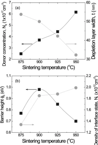
Fig. 6 shows the modified capacitance-voltage(C-V) characteristics of the samples sintered at various tempera- tures. The C-V characteristic parameters, such as donor concentration(N
d), barrier height( Φ
b), and density of interface states(N
t) are determined from Fig. 6. Changing tendency of donor concentration(N
d) and depletion layer width (t) as a function of sintering temperature was indicated graphically in Fig. 7(a). The N
dincreased in the order of 2.49 × 10
17, 3.70 × 10
17, 4.44 × 10
17, and 6.16 × 10
17cm
−3with the increase of sintering temperatures. The increase of N
dvalue is assumed to be due to the dis- sociation of zinc oxide through the expression, ZnO → Zn
ix+ 1/2O
2, Zn
ix→ Zn
i●
+ e' where Zn
ix
is a neutral zinc of interstitial site, Zn
i●
is a positively charged zinc
Fig. 6. C-V characteristics of the samples sintered at various tem- peratures.Fig. 4. E-J characteristics of the samples sintered at various tem- peratures.
Fig. 5. Nonlinear coefficient and leakage current density as a function of sintering temperature.
ion of interstitial site. It is assumed that the increase of the donor density is attributed to a lot of dissociation quantities of zinc oxide when the sintering temperature increased. The depletion layer width (t) value on both sides of depletion region at the grain boundary decreased in the order of 53.8, 50, 4.23, and 32.3 nm due to the increase of donor density with increasing sintering tem- perature. It can be seen that changing tendency of t is opposite to that of N
d. In general, the depletion region extends farther into the side with a lighter addition.
Changing tendency of barrier height( Φ
b) and density of interface states(N
t) as a function of sintering temperature was indicated graphically in Fig. 7(b). As the sintering temperature increased, Φ
bincreased from 0.77 to 0.98 eV until the sintering temperature is 900
oC. The maximum Φ
bvalue(0.98 eV) was obtained at 900
oC. When the sintering temperature exceeded 900
oC, Φ
bdecreased to 0.70 eV at 950
oC. This coincides with the behavior of α value in V-I characteristics. Really, the higher barrier gives rise to the higher nonlinear coefficient. N
tincreased in the order of 1.34 × 10
12, 1.85 × 10
12, 1.88 × 10
12, and 1.99 × 10
12cm
−2with increasing sintering temperature. N
tis directly associated with the N
dand Φ
bbecause the N
tis proportional to . In other words, N
tis estimated by the variation rate in the N
dand Φ
b. In general, N
tis increased with increasing N
tand decreasing N
d.
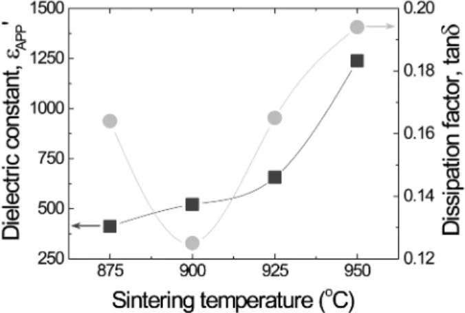
Fig. 8 shows the dielectric constant( ε
APP') and dissipation factor(tan δ) of the samples sintered at various tem- peratures. The ε
APP' of all samples decreased when the frequency increased from 10
2to 10
6Hz. It is assumed that the decrease of ε
APP' with increasing frequency is attributed to the decrease of the number of dipole, which can follow to test frequency. ε
APP' increased in the range of overall frequency with increasing sintering temperature.
This is directly related to the average grain size and depletion layer width, as can be seen through the following, ε
APP' = ε
g(d/t), where ε
gis the dielectric con- stant of ZnO(8.5), d is the average grain size, and t is the depletion layer width of the both sides at the grain boundaries. Changing tendency of dielectric constant( ε
APP') and dissipation factor(tan δ) as a function of sintering temperature was indicated graphically in Fig. 9. ε
APP' at 1 kHz increased in the order of 412.3, 521.4, 656.9, and 1238.4 with increasing sintering temperature. This attri-
NdΦb
Fig. 8. Dielectric characteristics of the samples with different sintering temperatures.
Fig. 7. (a) Donor concentration and density of interface states, and (b) barrier height and depletion layer width as a function of sintering temperature.
42 Choon-Woo Nahm
buted to the increase of donor density, and the decrease of depletion layer width, as describes previously, when the sintering temperature increased. On the other hand, the behavior of tan δ in accordance with signal frequency is more complex than the behavior of ε
APP'. tan δ for all samples decreased exponentially up to a specified fre- quency with increasing the frequency: 11.7 kHz at 875
o
C, 6.1 kHz at 900
oC, 13.1 kHz at 925
oC, and 20.0 kHz for 950
oC. Thereafter, tan δ increased up to a specified frequency with increasing the frequency: 763.2 kHz at 875
oC, 497.4 kHz at 900
oC, 446.9 kHz at 925
oC, and 324.1 kHz at 950
oC, and then exhibited the decreasing tendency when the frequency further increased. As the sintering temperature increased, tan δ at 1 kHz decreased from 0.164 to 0.125 until the sintering temperature is 900
oC. When the sintering temperature exceeded 900
oC, tan δ increased to 0.194 at 950
oC. This is similar with the behavior of J
Lwith increasing sintering temperature.
Among joule heating loss by leakage current and friction loss by dipole rotation, tan δ seem s to be affected by former.
4. Conclusions
This study has investigated how sintering temperature has an effect on the microstructure, electrical and dielectric properties of (V, Mn, Co, Dy, Bi)-codoped zinc oxide varistor ceramics. With the sintering temperature varying from 875 to 950
oC, it increased the average grain size, whereas it decreased the density of sintered pellets by
volatilizing V-species. Electrically, the breakdown field decreased with the increase of sintering temperature. The nonlinear coefficient increased when the sintering tem- perature was increased from 875
oC to 900
oC, and then increased when the sintering temperature was further increased. The most important feature of this system is low leakage current(36.4 μA/cm
2) at 900
oC in the sintering temperature. The increase of sintering temperature was confirmed to increase the donor concentration.
References
1. G. D. Mahan, J. Appl. Phys., 54(7), 3832 (1983).
2. M. Matsuoka, Jpn. J. Appl. Phys., 10(6), 736 (1971).
3. L. M. Levinson and H. R. Philipp, Am. Ceram. Soc.
Bull., 65(4), 639 (1986).
4. T. K. Gupta, J. Am. Ceram. Soc., 73(7), 1817 (1990).
5. K. Mukae, Am. Ceram. Bull., 66(10), 1329 (1987).
6. K. Mukae, K. Tsuda, and S. Shiga, IEEE T. Power Deliver, 3(2), 591 (1988).
7. K. Mukae, K. Tsuda, and I. Nagasawa, Jpn. J. Appl.
Phys., 16, 1361 (1977).
8. C. -W. Nahm, Mater. Lett., 47(3), 182 (2001).
9. J. -K. Tsai and T. -B. Wu, J. Appl. Phys., 76(8), 4817 (1994).
10. J. -K. Tsai and T. -B. Wu, Mater. Lett., 26(3), 199 (1996).
11. C. T. Kuo, C. S. Chen and I. -N. Lin, J. Am. Ceram.
Soc., 81(11), 2949 (1998).
12. H. -H. Hng and K. M. Knowles, J. Am. Ceram. Soc., 83(10) 2455 (2000).
13. H. -H. Hng and P. L. Chan, Mater. Chem. Phys., 75(1- 3), 61 (2002).
14. H. -H. Hng and P. L. Chan, Ceram. Int., 30, 1647 (2004).
15. C. -W. Nahm, J. Mater. Sci., 42(19), 8370 (2007).
16. C. -W. Nahm, Ceram. Int., 35(8), 3435 (2009).
17. C. -W. Nahm, Ceram. Int., 36(3), 1109 (2010).
18. C. -W. Nahm, J. Alloys Compd., 509(34), L314 (2011).
19. C. -W. Nahm, J. Mater. Sci.: Mater. Electronic., 24(1), 27 (2013).
20. C. -W. Nahm, J. Mater. Sci.: Mater. Electronic., 24(1), 70 (2013).
21. C. -W. Nahm, Mater. Sci. Semicon. Process., 16(5), 1308 (2013).
22. J. C. Wurst and J. A. Nelson, J. Am. Ceram. Soc., 55(97- 12), 109 (1972).
23. M. Mukae, K. Tsuda, and I. Nagasawa, J. Appl. Phys., 50(6), 4475 (1979).
Fig. 9. Dielectric constant and dissipation factor as a function of sintering temperature.