• 검색 결과가 없습니다.

Assessment Methodology of Junction Temperature of Light-Emitting Diodes (LEDs)

N/A
N/A
Protected

Academic year: 2021

Share "Assessment Methodology of Junction Temperature of Light-Emitting Diodes (LEDs)"

Copied!
8
0
0

로드 중.... (전체 텍스트 보기)

전체 글

(1)

Assessment Methodology of Junction Temperature of Light-Emitting Diodes (LEDs)

Moon-Hwan Chang

and Michael Pecht

Center for Advanced Life Cycle Engineering, Department of Mechanical Engineering, University of Maryland, College Park, MD 20742

(Received April 4, 2016: Corrected May 24, 2016: Accepted July 22, 2016)

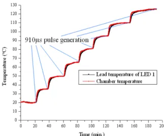
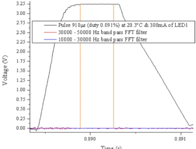
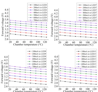
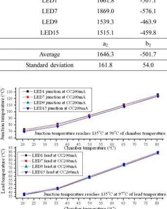
Abstract: High junction temperature directly or indirectly affects the optical performance and reliability of high power LEDs in many ways. This paper is focused on junction temperature characterization of LEDs. High power LEDs (3W) were tested in temperature steps to reach a thermal equilibrium condition between the chamber and the LEDs. The LEDs were generated by pulsed currents with duty ratios (0.091% and 0.061%) in multiple steps from 0mA and 700mA. The diode forward voltages corresponding to the short pulsed currents were monitored to correlate junction temperatures with the forward voltage responses for calibration measurement. In junction temperature measurement, forward voltage responses at different current levels were used to estimate junction temperatures. Finally junction temperatures in multiple steps of currents were estimated in effectively controlled conditions for designing the reliability of LEDs.

Keywords: Light-emitting diode, Reliability, Junction temperature

1. Introduction

High-power LEDs are used for a wide variety of applica- tions, such as display backlighting, communications, med- ical services, signage, and general illumination.

1-8)

LEDs offer design flexibility; easy adjustment of line-scale, area- scale, and color dimming; high energy efficiency resulting in low power consumption; long lifetimes up to 50,000 hrs;

micro-second-level on-off switching enabling ultrahigh speed response time; wide range of color temperature; and no low-temperature startup problems.

The LED industry, despite exciting innovations driven by technological advances and ecological/energy-saving concerns, still faces a challenge in attracting widespread adoption. The issue of concern is the lack of information and confidence regarding reliability. Data sheets of manu- facturers provide user information on optical and electrical characteristics of high power LEDs at room temperature (or 25

o

C junction temp.) or thermal resistance including package and built on printed circuit board. This informa- tion cannot guarantee the performance and reliability of high power LEDs because usage conditions of LED based electronic products are not matched with the conditions in the data sheets. Absolute maximum rating of junction tem- perature on data sheets is either 125

o

C or 135

o

C. Users are

required to design LED packages (and products) within this junction temperature guideline.

The LED die is a semiconductor, and the nature of man- ufacturing of LED packages is similar to that of micro- electronics. But there are unique functional requirements, materials, and interfaces in LEDs resulting in different fail- ure modes and mechanisms. The failure sites of LEDs are dies, interconnects, and packages. The die-related failures are severe light output degradation and burned or broken metallization on the die. The interconnect failures of LED packages are electrical overstress-induced bond wire frac- ture and wire ball bond fatigue, electrical contact metallur- gical interdiffusion, and electrostatic discharge, which leads to catastrophic failures of LEDs. Package-related failure mechanisms include carbonization of encapsulant, encapsulant yellowing, delamination, lens cracking, phos- phor thermal quenching, and solder joint fatigue. These result in optical degradation, color change, electrical opens/

shorts, and severe discoloration of the encapsulant. Many of these failures are related to thermal stress as well as electrical stress and hygromechanical stress. Thermal stress affects die cracking, wire ball bond fatigue, delamination, lens cracking, encapsulant yellowing, and phosphor ther- mal quenching. The failure modes of LEDs relate to light output and optical characteristics as well as change of elec-

Corresponding author

E-mail: [email protected]

© 2016, The Korean Microelectronics and Packaging Society

This is an Open-Access article distributed under the terms of the Creative Commons Attribution Non-Commercial License(http://creativecommons.org/

licenses/by-nc/3.0) which permits unrestricted non-commercial use, distribution, and reproduction in any medium, provided the original work is

properly cited.

(2)

trical parameters. These modes differentiate LEDs from the failure modes of other electronic parts where the failures are generally related to electrical parameter degradation.

When a high current is applied to LEDs, there is increased light output. The problem is that light output can change as a result of operating conditions, temperature in particular. Light output decreases with a temperature rise in LEDs, since quantum efficiency decreases at higher tem- peratures, which contributes to more non-radiation recom- bination events in LEDs.

9)

A temperature increase is also related to forward voltage decrease in the I-V curve due to a decrease in the bandgap energy of the active region of LEDs and also due to a decrease in series resistance occur- ring at high temperatures. The resistance decrease is due to higher acceptor activation occurring at elevated tempera- tures as well as the resulting higher conductivity of the p- type layer and active layers. In addition to the quantum efficiency drop, the color of the LEDs also changes. In par- ticular, phosphor-converted LEDs with blue InGaN and yellow phosphors experience light output degradation, which causes shifts of blue peak wavelength toward longer wavelengths and shifts of the peak energy of the phosphors to lower wavelengths when the temperature of the LEDs increases. The shifts of the blue peak wavelength toward longer wavelengths having lower energy are due to the junction temperature dependence of energy gap shrinkage.

The peak energy shifts of the phosphors are due to phos- phor thermal quenching. To sum up, many important reli- ability-related features of LEDs are a function of temper- ature.

High power LEDs’ long-term stability and lifetime are typically judged on the basis of measured light output. The measured light output mostly depends on the junction tem- perature. Hence, the reliability of light output measure- ments is determined by the temperature stability of the light output measurement setup and by the accuracy of the temperature measurement. Prediction of the junction tem- perature is complicated, and there are associated uncertain- ties, as it is junction temperature is measured in an indirect way by measuring the temperatures of reference points on leads or metal heat slugs and utilizing them to estimate the junction temperature.

Thermal stressing of LEDs directly or indirectly by high junction temperature affects internal efficiency, maximum light output, reliability, peak wavelength, and spectral wavelength.

10)

When a drive current is applied to an LED, the LED junction produces heat, and heat then flows through the junction to the outside of the junction. An accurate method of measuring junction temperature is

required to make sure that critical high temperatures beyond the absolute maximum ratings are avoided.

The ideal way to measure junction temperature is to measure the device temperature as close as possible to the heat source. One method that could be used is to place a temperature sensor very close to the junction and measure the sensor signal. This is straightforward, but there are physical limitations to this technique due to the finite size of the sensor and the encapsulated seal of the LED die around LED package. In many cases, the sensor itself is larger than the junction to be measured. This adds error to the measurement affecting the accuracy of the measure- ment.

11)

Various indirect techniques and models have been attempted to estimate the junction temperature of laser diodes, including micro Raman spectroscopy, threshold voltage, thermal resistance, photo thermal reflectance microscopy, electroluminescence, and photoluminescence.

10)

Chhajed et al.

10)

demonstrated that the diode forward voltage method is the most accurate method and can be used to estimate the junction temperature of LED pack- ages. In a few previous researches, the diode forward voltage has been used to assess the junction temperature of the pn-junction diode of LEDs.

11-13)

The forward-voltage method is made up of two series of measurements, a calibration measurement and an actual junction temperature measurement. Calibration measurement by using a pulse current serves as a reference for junction temperature equal to ambient (chamber) temperature and establishes the relation between the forward voltage and the junction temperature. Actual junction temperature measurement uses constant current adding the Joule heating effect to LEDs and derives the relation between the forward voltage and the junction temperature. In the calibration measure- ment, a pulsed forward current (with a duty cycle of 0.1%) drives LED samples

10-12)

to ensure that the junction tem- perature is equal to the ambient temperature.

Prognostics and health management (PHM) techniques estimate lifetime of LEDs with in-situ monitoring parame- ters such as forward voltage, lead temperature, forward current, light output, and color. PHM techniques take advantage of the advances in prognostic methods including sensor technologies, data collection, storage and distribu- tion, analysis of multi-parameter data, and understanding of failure mechanisms without changing failure modes of LEDs to reduce time for qualification and provide addi- tional information towards determining reliability in field.

The development and utilization of this method can also

lead to methods of implementing prognostics during appli-

(3)

cation. In-situ monitoring of forward voltage enables to estimate junction temperature with real time at usage con- ditions to investigate junction temperature impact on tem- perature aging test or power aging test in further researches of LEDs.

In this paper, the assessment of junction temperature of LEDs was conducted with tests and measurement instruments This work shows that 200 steps of pulse with 0.061% duty ratio are used to estimate junction tempera- ture for high power LEDs. Once obtained results of multi- current steps for all range of operating currents, junction temperature at specific current and ambient temperature can be derived without experiments at each single current.

2. Experiment: Devices and Process

For the test using the forward voltage method, sixteen high power InGaN LEDs (labeled as LED1, LED2, and so on) with maximum absolute junction temperature ratings of 135

o

C were selected and mounted on an aluminum metal core printed circuit board (MCPCB). The LED pack- age is composed of LCP (liquid crystal polymer) represent- ing the case material and Cu representing the leads. An overview of an LED package under test is shown in Fig. 1.

The size of the LCP case is 4 mm × 4 mm × 0.8 mm with 1.0 mm height of the hemispherical silicone lens. There are three leads for the anode side and three for the cathode side. Each lead is 0.65 mm in length, 0.60 mm in width, and 0.30 mm in thickness. The middle lead on each anode and cathode side is used for an electrical connection with the aluminum MCPCB. The metal heat slug is located at the center of the LED package to provide a mechanical connection and a thermal path to the aluminum MCPCB.

An MCPCB (LED board) consists of a base layer (alu- minum), a dielectric layer (FR-4 layer), and a circuit layer (Cu trace layer) for higher heat dissipation than the FR-4 board in this study. The MCPCB dimensions are 223 mm × 105 mm × 1.615 mm, as shown in Fig. 2. The thickness of each layer was 1.5 mm (aluminum), 0.085 mm (FR-4), and 0.03 mm (Cu trace). The percent of metallization of the Cu trace circuit layer was 13.2% based on the area calculation of the Cu trace of the MCPCB for LEDs. Sixteen LEDs are

directly mounted in contact with the surface of the top Cu trace layer of the aluminum MCPCB. The interconnect material, i.e., solder paste, was 62% Sn, 36% Pb, and 2%

Ag. The dimensions of the solder joint are 0.12 mm (solder joint height), 0.12 mm (standoff height), and 0.26 mm

2

(solder joint bond area). The pitch between each LED is 25 mm in each direction.

An LED test board circuit is described in Fig. 3. A

1

con- nects LED1 and LED2 serially to measure the current of the serial connections and light up these LEDs. V

1

and V

2

are used to measure voltages across each LED. In each cal- ibration measurement, two LEDs (dotted boxes in Fig. 2) were lighted by a sourcemeter. Thermocouple wires were attached to the anode side of leads for the tested LEDs. An overview of the test setup is shown in Fig. 4. In the tests, the LED board was placed in a temperature chamber (Rus- sells chamber (RB-16-3-3-LN2) and connected to a sourcemeter (Keithley 2410) generating a short pulse (910 µs), a DAQ board (NI USB 9215) collecting forward volt- age responses, and a data logger (Agilent 34970A) moni- toring the lead temperatures. A Labview-controlled computer set was used to program a 910 µs short pulse and monitor LED responses from a Keithley 2410 sourcemeter, NI USB 9215 DAQ board, and Agilent 34970A data log- ger. Four LEDs (LED1, LED7, LED9, and LED15) were selected and tested to reflect the location difference in the MCPCB. In each test, two LEDs (dotted box) were lighted Fig. 1. Schematic view and bottom view of LED package.

Fig. 2. Tested LED samples in Al metal core printed circuit board.

Fig. 3. Concept of LED test board circuit.

(4)

by using a Keithley 2410 sourcemeter.

In the calibration measurement, the LED board was placed into the temperature chamber. The chamber was set at different temperature steps (20

o

C, 35

o

C, 50

o

C, 65

o

C, 80

o

C, 95

o

C, 110

o

C, and 125

o

C). LED lead temperatures and chamber temperatures were monitored every second by using an Agilent 34970 data logger. 910 µs pulses were generated on LEDs twice every 3 seconds by using a Lab- view-controlled Keithley 2410 sourcemeter after confirm- ing that the lead temperature of the LEDs was the same as the chamber temperature (i.e., thermal equilibrium condi- tion). The duty ratio was 0.061% (for 200 peak current lev- els from 0 mA to 700 mA) or 0.091% (for a single current level). Voltage responses were stored via a NI 9215 DAQ board with 300 k data in 3 seconds. Chamber temperature was increased to the next step. The steps were repeated until the chamber temperature reached 125

o

C. In the cali- bration measurement, a V

f

(forward voltage) vs. T

a

(ambi- ent temperature) plot was obtained at the thermal equi- librium condition between the LED junction and the ambi- ent temperature without storing Joule heating into LEDs using 910 µs current pulse generation.

In the junction temperature measurement, junction tem- peratures at each constant current and chamber temperature (aging test conditions) were estimated by the in-situ moni- toring forward voltage responses and lead temperatures of LEDs every second. The variation of constant current was also monitored by a data logger each second to make sure that the constant current was maintained with an initial setup value. Test currents are used of 200 mA and 300 mA constant currents. The constant currents loaded into LEDs were the same as the peak current in pulse operation.

Chamber temperatures were used at 20

o

C, 35

o

C, 50

o

C, 65

o

C, and 80

o

C for 200 mA. Chamber temperatures were selected at 20

o

C, 35

o

C, 50

o

C, and 65

o

C for 300 mA. At each stage of the chamber temperature condition, 30 min- utes for lighting the LEDs were needed to achieve a stable

forward voltage. The junction temperature was then esti- mated by using the previously obtained T

a

vs. V

f

plot.

3. Experiment Results and Discussion

3.1. Calibration Measurement

The dwell time of each temperature is around 20 min- utes. The dwell time was determined experimentally, and it turned out that 20 minutes was sufficient to reach the ther- mal equilibrium condition for the LED package and ambi- ent temperature. The dwell time was longer when the chamber temperature was 110

o

C and 125

o

C, as shown in Fig. 5. Pulse generation was made when the lead tempera- ture of the LED was equal to the chamber temperature (at thermal equilibrium) conditions, as shown in Fig. 5.

After the junction has come to thermal equilibrium, a pulsed current of 910 µs duration with a duty ratio 0.091%

was sourced into LEDs and the voltage response was mea- sured, as shown in Fig. 6. A sampling rate of 300,000 data was used for 3 seconds to detect the output signal and aver- age the voltage responses during 910 µs. A Fast Fourier Transform (FFT) was performed to average the forward voltage response at each pulse, as shown in Fig. 7. The main pulse was 0 Hz, 20,000 Hz, and 40,000 Hz. 0 Hz cor- responds to the near zero volts mostly obtained during 3 seconds of data recording time through the DAQ board.

The specific zone depicted in Fig. 8 was used to determine forward voltage response at each pulse to avoid the 20,000 Hz and 40,000 Hz components, which are regarded as the main sources of noise.

To verify pulse duration, a constant current of 700 mA (maximum absolute rating from the manufacturer’s data sheet) was applied until it reached the maximum tempera- ture of lead at an ambient temperature of 21.5

o

C. The Fig. 4. Overview of test setup.

Fig. 5. Ambient temperature profile.

(5)

ambient temperature was chosen because the change of the lead temperature at 21.5

o

C can be shown more clearly than changes at higher ambient temperatures. The temperature increased linearly until the time reached 0.28 minutes, as shown in Fig. 9. During the initial 0.28 minutes, the lead temperature increased up to 33.8

o

C. Therefore, temperature elevation during 0.28 minutes was calculated as 11.5

o

C.

The temperature change of the lead at 910 µs was evalu- ated as 0.00062

o

C. If we assume that the junction tempera-

ture increases corresponding to the elevation of the lead temperature, a 910 µs pulse duration was fairly short to avoid Joule heating from the p-n junction diode of the 3W high-power LEDs.

Further experiments were conducted using a verified Fig. 6. Forward voltage response from 910 µs pulse duration.

Fig. 7. Fast Fourier Transform of pulse response.

Fig. 8. Forward voltage determination at each pulse.

Fig. 9. Pulse duration verification at 25

o

C ambient temperature with 700 mA constant current.

Fig. 10. I-V curves obtained from 200 steps of single pulse

generated by 910 µs pulse and 0.061% duty ratio.

(6)

short pulse, 910 µs. 200 steps of pulse were applied at each chamber temperature with a 910 µs pulsed current and a 0.061% duty ratio by using a single pulse in each step, as shown in Fig. 10. Without storing the Joule heating effect of LEDs, the forward voltages at different ambient tem- peratures as reference values can be used for estimating the junction temperature of LEDs at any specific current among 200 different current levels from 0 to 700 mA. Fig.

11 shows V

f

(forward voltage) vs. T

a

(ambient tempera- ture) plots obtained linearly from these multi-steps of 910

µs pulse and chamber temperature (20

o

C, 35

o

C, 50

o

C, 65

o

C, 80

o

C, 95

o

C, 110

o

C, and 125

o

C). 200 steps of the I-V pulse curve also showed that when the ambient tempera- ture (the same as the junction temperature) was higher, the forward voltage response went lower and the slope in I-V curve became steeper.

T

j

vs. V

f

linear fits were plotted for each tested LED, as shown in Fig. 12. The calculated values of the slopes and intercepts in the duty ratio 0.091% were compared with the values of the slopes and intercepts in the duty ratio 0.061%, as shown in Table 1. It turned out that the average values and standard deviations of the slope a2 and intercept b2 from 300 mA result obtained by 200 steps of 910 µs pulse with 0.061% duty are similar to average values and standard deviations of the slope a1 and intercept b1 from a single current level (at 300 mA) with 0.091% duty ratio.

This result confirmed that 200 steps of pulse with a 0.061% duty ratio can be practically used to construct a reference plot of T

j

vs. V

f

at a specific current level between 0 mA to 700 mA. The minor difference was caused by the variation of chamber temperature in the experiments. The variation of the chamber temperature was 0.4

o

C at each step of the ambient temperatures. The slopes and intercepts of the linear fits for T

j

vs. V

f

relation- ship at 200 mA with a 0.061% duty ratio were evaluated using data from 200 step-pulsed currents in Table 2. We assume that LED 7 had relatively larger values of slopes Fig. 11. Forward voltage vs. chamber temperature.

Fig. 12. Linear fits of T

j

vs. V

f

in duty ratio 0.091% and 0.061%.

(7)

and intercepts because LED 7 came from a different LED binning lot from the manufacturer than the other tested LEDs.

3.2. Junction Temperature Measurement

In Fig. 13, the forward voltage responses at 200 mA show the natural response voltages of each LED while the voltage responses at 300 mA show that the Joule heating effect changes the voltage characteristics of LEDs. A con-

stant current of 200 mA can be used to investigate how high power LEDs change in a high temperature environ- ment while minimizing heat generation from the LED die itself. A 300 mA constant current is useful to combine the high ambient temperature effect and the Joule heating effect from LEDs.

The test results of junction temperature measurement at a Table 1. Comparison of slope and intercept at 300 mA between 0.091% duty test result and 0.061% duty test result

T

j

= a

1

+ b

1

× V

f

T

j

= a

2

+ b

2

× V

f

Duty ratio 0.091% at 300 mA Duty ratio 0.061% at 300 mA

a

1

b

1

a

2

b

2

LED1 1655.9 -506.0 LED1 1661.8 -507.1

LED7 1881.4 -580.9 LED7 1869.0 -576.1

LED9 1535.6 -463.6 LED9 1539.3 -463.9

LED15 1509.1 -458.6 LED15 1515.1 -459.8

a

1

b

1

a

2

b

2

Average 1645.5 -502.3 Average 1646.3 -501.7

Standard deviation 169.8 56.6 Standard deviation 161.8 54.0

Table 2. Slope and intercept at 200 mA with a 0.061% duty ratio T

j

= a

3

+ b

3

× V

f

Duty ratio of 0.061% at 200 mA

a

3

b

3

LED1 1558.6 -498.6

LED7 1859.3 -603.8

LED9 1481.1 -469.8

LED15 1491.2 -476.1

a

3

b

3

Average 1597.6 -512.1

Standard deviation 177.9 62.4

Fig. 13. Forward voltage response at constant current (CC) 200 mA and 300 mA.

Fig. 14. Junction temperature measurement at constant current 200

mA.

(8)

constant current of 200 mA demonstrated that the junction temperature reached the maximum absolute rating of 135

o

C at a chamber temperature of 90

o

C and 97

o

C of lead temperature, as shown in Fig. 14. The junction temperature reached 135

o

C at 65

o

C of chamber temperature and 74

o

C of lead temperature, as shown in Fig. 15.

4. Conclusions

This work shows that 200 steps of pulse with 0.061%

duty ratio can be used to estimate junction temperature for high power LEDs. This approach uses direct way of esti- mation of junction temperature by considering forward voltage and junction temperature. This approach doesn’t need to use temperature data of reference points like previ- ous thermal resistance approach. Also, once obtained results of multi-current steps for all range of operating cur- rents, junction temperature at specific current and ambient temperature can be derived without experiments at each single currents. Previous approach cannot obtain junction temperatures at different current levels as it derives junc- tion temperature at single current. This result helps design- ers and customers to estimate junction temperature without uncertainties existed in current methods. Current JEDEC Standard 51-1 standard should be changed for thermal measurement method and modeling methods for LED packages. The new standard needs common means for comparing junction temperature values with different types/

manufacturers of LEDs for users.

References

1. M. R. Krames, O. B. Shchekin, R. Mueller-Mach, G. O.

Mueller, L. Zhou, G. Harbers and M. G. Craford, “Status and Future of High-Power Light-Emitting Diodes for Solid-State Lighting”, J. Display Technol., 3(2), 160 (2007).

2. D. A. Steigerwald, J. C. Bhat, D. Collins, R. M. Fletcher, M.

O. Holcomb, M. J. Ludowise, P. S. Martin and S. L. Rudaz,

“Illumination with Solid State Lighting Technology”, IEEE J.

Sel. Topics Quantum Electron., 8(2), 310 (2002).

3. F. M. Steranka, J. Bhat, D. Collins, L. Cook, M. G. Craford, R. Fletcher, N. Gardner, P. Grillot, W. Goetz, M. Keuper, R.

Khare, A. Kim, M. Krames, G. Harbers, M. Ludowise, P. S.

Martin, M. Misra, G. Mueller, R. Mueller-Mach, S. Rudaz, Y.- C. Shen, D. Steigerwald, S. Stockman, S. Subramanya, T.

Trottier and J. J. Wierer, “High Power LEDs-Technology Sta- tus and Market Applications”, Phys. Status Solidi A, 194(2), 380 (2002).

4. Y. Aoyama and T. Yachi, “An LED Module Array System Designed for Streetlight Use”, Energy 2030 Conference, 2008. Energy 2008. IEEE, 1 (2008).

5. R. Vittori and A. Scaburri, “New Solid State Technologies and Light Emission diodes as a Mean of Control and Lighting Source Applicable to Explosion Proof Equipment, With the Scope to Reduce Maintenance, to Limit the Risk of Bad Maintenance and to Expand the Plants’ Life”, PCIC Europe, 2009. PCIC EUROPE’09. Conference Record, 193 (2009).

6. J.-B. Park, H.-J. Park, T. Jeong, S.-J. Kang, J.-S. Ha, and S.- J. Leem, “Study on the Electrode Design for an Advanced Structure of Vertical LED”, J. Microelectron. Packag. Soc., 22(4), 71 (2015).

7. T.-Y. Lee, K.-H. Kim, M.-S. Kim, E.-S. Ko, J.-H. Chio, K.- S. Moon, M.-S. Kim and S. Yoo, “Light Efficiency of LED Package with TiO

2

-Nanoparticle-Dispersed Encapsulant”, J.

Microelectron. Packag. Soc., 21(3), 31 (2014).

8. W. Kim, H. S. Kim, D. Shin and H. C. Lee, “Effects of ZnO Composition on the Thermal Emission Properties for LTCC Type of High Power LED Package”, J. Microelectron.

Packag. Soc., 19(4), 79 (2012).

9. J. Liu, W. S. Tam, H. Wong and V. Filip, “Temperature- Dependent Light-Emitting Characteristics of InGaN/GaN Diodes”, Microelectron. Reliab., 49(1), 38 (2009).

10. S. Chhajed, Y. Xi, T. Gessmann, J.-Q. Xi, J. M. Shah, J. K.

Kim and E. F. Shubert, “Junction Temperature in Light-Emit- ting Diodes Assessed by Different Methods”, Proc. SPIE, 5739, Light-Emitting Diodes: Research, Manufacturing, and Applications IX, San Jose, California, 16 (2005).

11. J. Chonko, “Using Forward Voltage to Measure Semiconduc- tor Junction Temperature”, Keithley Instruments, Inc., 2681, 1 (2006).

12. Y. Xi and E. F. Schubert, “Junction-temperature Measurement in GaN Ultraviolet Light-emitting Diodes Using Diode For- ward Voltage Method”, Appl. Phys. Lett., 85(12), 2163 (2004).

13. F. Jiang, W. Liu, Y. Li, W. Fang, C. Mo, M. Zhou and H. Liu,

“Research on the Junction-temperature Characteristic of GaN Light-emitting Diodes on Si Substrate”, J. Lumin., 122-123, 693 (2007).

Fig. 15. Junction temperature measurement at constant current 300

mA.

수치

Fig. 2. Tested LED samples in Al metal core printed circuit board.
Fig. 5. Ambient temperature profile.
Fig. 10. I-V curves obtained from 200 steps of single pulse generated by 910  µs pulse and 0.061% duty ratio.
Fig. 12. Linear fits of T j  vs. V f  in duty ratio 0.091% and 0.061%.
+3

참조

관련 문서

Upon thermal contact between two objects at different temperature, thermal energy transfers from the object at higher temperature to the other object at lower temperature

average forward current forward power dissipation 2.5 The complete diode model 2.6 Diode

The index is calculated with the latest 5-year auction data of 400 selected Classic, Modern, and Contemporary Chinese painting artists from major auction houses..

The “Asset Allocation” portfolio assumes the following weights: 25% in the S&P 500, 10% in the Russell 2000, 15% in the MSCI EAFE, 5% in the MSCI EME, 25% in the

1 John Owen, Justification by Faith Alone, in The Works of John Owen, ed. John Bolt, trans. Scott Clark, "Do This and Live: Christ's Active Obedience as the

In this thesis, we studied the enhancement of the light extraction efficiency in InGaN-based light-emitting diodes (LEDs) patterned with nano structures.. The

In order to analyze thermal stability and capacity loss according to the temperature of the battery cell by applying different C-rate discharge and

The data are corrected for temperature error due to solar radiation and the effect of low temperature on the anerod capsule and curvature of the surface of